Growth by the Heat Exchanger Method and Characterization of Multi-crystalline Silicon ingots for PV
←
→
Page content transcription
If your browser does not render page correctly, please read the page content below
Rev. Energ. Ren. Vol. 8 (2005) 49 - 54

                     Growth by the Heat Exchanger Method and
               Characterization of Multi-crystalline Silicon ingots for PV

                          D. Ouadjaout, Y. Gritli, L. Zair and M. Boumaour

                              Unité de Développement de la Technologie du Silicium
                               2, Bd Frantz Fanon, B.P. 399, Alger - Gare, Algérie

      Abstract - Multi-crystalline silicon ingots of 44 cm square cross section, weighing 80 kg, have
      been produced by a modified Heat Exchanger Method in which a graphite insulation and heat
      exchanger block move down from the heater during crystal growth to facilitate heat extraction
      from the bottom of the crucible. Wafers of 300 µm thickness and 1.2 Ω-cm resistivity, have shown
      consistency and uniformity in the properties required for large-scale production. The interstitial
      oxygen concentration varies from 1.6 to 3.6 ppm, whereas the substitutional carbon concentration
      is assessed to be below 10 ppm.
      Résumé - Nous avons utilisé une variante de la technique de l’échangeur thermique (HEM) pour
      élaborer des lingots de silicium multicristallin à usage photovoltaïque. Au lieu d’utiliser l’hélium
      comme agent d’extraction de la chaleur, la solidification directionnelle est, dans notre cas,
      provoquée par l’abaissement, durant le cycle de croissance, du bloc de graphite situé sous le
      creuset. Le matériau obtenu semble présenter les propriétés requises à une production à grande
      échelle.
      Keywords: Multi-crystalline silicon – Characterization - Directional solidification - Photovoltaic.

                                          1. INTRODUCTION
   The photovoltaic industry is presently growing at 40 % per year, largely due to government
subsidised programs. A recent market survey reports that, of all solar photovoltaic module
sales in 2002, 36 % were based on mono-crystalline silicon wafers, similar to those used in
microelectronics. A further 52 % were based on lower-quality multi-crystalline silicon wafers.
These are large-grained polycrystalline wafers produced by slicing from large ingots of
directionally solidified silicon, an approach developed specifically for photovoltaic [1].
   With increasing expectations for the solar cell market, a shortage of the silicon material is
forecasted [2]. This tendency will continue into the near future. Since silicon wafer costs
constitute a large portion of the total cost, several technologies have been competing for the
low-cost production of silicon wafers. The Czochralski (CZ) technology is considered to be
the first one to meet this goal. However, in terms of yield and productivity, CZ technology
has the drawback of the labour-intensive ‘‘seeding’’ step. Heat exchange method (HEM) is
the other strong candidate for low-cost production [3]. The process control for the production
of large multi-crystalline silicon ingot is easier than in CZ technology.
    Another advantage is the in situ annealing of the ingot after growth. This in situ annealing
reduces the thermal stresses which cause dislocation generation in the ingot. Originally, HEM
technology was developed to grow single-crystalline materials with seeding. However, multi-
crystalline silicon crystal grown in small size with HEM without seeding is found to have
almost the equivalent electrical property as mono-crystalline silicon for solar cells [4-6]. This
is due to vertically oriented grains which transport the carriers without hindrance in the crystal
grown with HEM. In this study, 80 kg multi-crystalline ingot is grown with fully automated
HEM furnace. The quality of the ingot is assessed with both Etch-Pits Density (EPD) analysis
and Fourier Transform Infrared (FTIR) spectroscopy.

                                                      49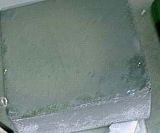
50 D. Oudjaout et al.
2. EXPERIMENTS
2.1 Crystal growth
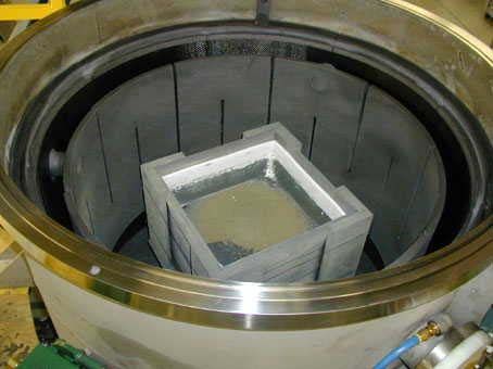
In this experiment, a HEM furnace manufactured by GT-Equipment Technologies Inc.
(Nashua, USA) is employed (Fig. 1). The furnace is well insulated. The graphite resistance
heating element provides heat so that there are no significant temperature variations during
the melt down of the silicon charge. The feedstock used for this charge was virgin solar grade
poly-silicon, having Acceptors concentration (Boron) < 0.3 ppb, Donors concentration
(Phosphorus) < 0.5 ppb and intrinsic Carbon concentration < 0.7 ppm.
Fig. 1: Interior of the UDTS / HEM furnace
During growth, the crucible is lowered in the heat zone to further facilitate heat extraction
from its bottom and to maintain low gradients. As can be seen (Fig. 2), the power is
maintained for 24 h during growth cycle. In this experiment, the growth rate averages
12mm/h, which is very close to that in the CZ process. The result is a large block of
crystallised silicon ingot (Fig. 3). This ingot is evaluated to see its acceptability in the solar
cell production.
2.2 Wafer processing
The obtained ingot is cut into sixteen 100 x 100 mm bricks by using a diamond wire saw.
After a crooping operation of 2 cm from top and bottom of all bricks, wafers with a thickness
of 300 µm are obtained by a multi wire saw machine using a mixture of silicon carbide with
glycol.
Batch of selected wafers from ingot are used to measure interstitial oxygen [Oi] and
substitutional carbon [Cs] concentrations, using FTIR spectroscopy. The resistivity of the
wafers is determined by mean of four probe technique. Other batches are used to determine
the EPD dislocation of the material.Growth by the Heat Exchanger Method and Characterization of Multi-crystalline Silicon… 51
1600 160
1400 140
1200 120
Temperature (°C)
1000 100
Power (KW)
800 80
600 60
400 40
200 20
0 0
0 3 7 10 13 17 20 23 27 30 33 37 40 43 47
Time (hours)
TOP PYROM TEMP HEX_TEMP MEASURED_POWER__ANALOG_INPUT_
Fig. 2: Main Process parameter data for a 44 x 44 x 18 cm silicon ingot
Fig. 3: 44 cm square cross section multi-crystalline silicon ingot
3. RESULTS AND DISCUSSION
3.1 Ingot evaluation
As can be seen in Fig. 3, cracks are not observed on the surface of the ingot. The top
surface is very smooth and, as suited, slightly convex. These observations indicate that a
strong unidirectional solidification takes place during the growth of this silicon crystal.
The slightly convex solid-liquid interface is confirmed by observing the circular solid
silicon first seen in the centre of the melt at the end of the growth cycle. This fact is due to the
temperature gradient created by opening and lowering respectively the insulation first, and
then the graphite heat exchanger block which is supporting the crucible. The solidification is52 D. Oudjaout et al.
initiated by extraction of the superheat from the bottom portion of the melt in the crucible;
this is accomplished by setting up the heat flow such that the heat extraction is primarily from
the bottom of the crucible and the heat input is such that no grains are nucleated along the
sidewalls. This situation is different from the casting process in which the solidification starts
from the crucible outside the melt and the crystal grows into the centre part of the melt. The
cooling situation in this process is also different from the CZ process where the cooling of the
ingot is conducted from outside the crystal, with argon gas flowing from the top of the
furnace. From this difference, it is expected that the ingot grown with this HEM furnace will
have less residual stress than the ingot grown by the CZ or casting process.
In Fig. 4, the grain morphology of the cross section of a brick is shown. As can be seen in
the picture, most of the grains are aligned vertically, i.e., the solidification proceeds in an
upward direction from the bottom of the crucible. This observation is coincident with the fact
that the top surface of the ingot is very flat. The vertical arrangement of the grains is very
favourable for solar cell fabrication because the grain boundary will not act as a barrier for the
electrical carriers generated. The other fact that can be seen in the picture is that the size and
shape of the grains is uniform throughout the ingot. This fact confirms the possibility that this
process is effective in the growth of large ingot. The upper part of the ingot is slightly bigger
than the lower part. It is possible that the slight deformation of the silicon crucible is due to
the long length of time which this process requires. Another possible explanation of these
results might be that the density of the solid silicon is lower than that of the liquid silicon.
Typical grain size
Fig. 4: Vertical cross section of a one brick of 44 cm multi-crystalline silicon ingot (side part)
As solidification proceeds, silicon can cause crucible deformation with increased volume.
Further, in the upper part of the ingot, grains nucleated from the side wall of the crucible can
be seen. Since the crucible becomes wider with the growth of the crystal, grains nucleated
from the bottom of the crucible might not be grown into this area. The grain morphology inGrowth by the Heat Exchanger Method and Characterization of Multi-crystalline Silicon… 53
this area is not better than that of the grains in the central area of the ingot. However, this part
will be removed during the preparation of the square ingot for the slicing.
As can be seen in Fig. 5, the average size of the grains is larger than 1 cm. The huge size of
the grains might be due to the lower growth rate of the crystal in this process. In the CZ
process, the growing ingot is pulled from the melt and cooled by the flowing of argon gas.
However, in this process, the solidified ingot is contained in the hot crucible and cooled down
slowly. Although not a single crystal as with CZ technology, the multi-crystalline ingot grown
in this process is believed to contain fully grown large grains. Because of these large grains,
the grain boundary is not expected to impair the efficiency of the solar cell later.
Fig. 5: Grain shape of 10 cm square multi-crystalline silicon wafer
3.2 Wafer characterization
A five minutes treatment with Shimmel etching solution was found to be a good
preparation of the samples for detecting dislocations and grain boundaries [7]. For this
purpose, EPD measurements have been performed using a light optical microscope combined
with a computer assisted image processing system. The data has been checked and corrected
manually. For a wafer close to those used for solar cell processing, an average EPD density of
6 105 cm-2 has been found. Twinned regions, like the one shown in Fig. 6, are typical crystal
defects of the investigated poly-Silicon wafers.
Prior to crystal growth, silicon has been doped with boron. Due to segregation phenomena
during growth, the measured wafer resistivity increases from 1.1 Ωcm close to the bottom part
of the crystal up to 1.3 Ωcm in the upper part, which corresponds to an average doping
concentration of 1.8 1016 at/cm3. FTIR spectroscopy reveals that the interstitial oxygen
concentration [Oi] varies from 1.6 to 3.6 ppm, whereas the substitutional carbon concentration
[Cs] is below 10 ppm. From these results, we can confirm the good quality of the batch
material.54 D. Oudjaout et al.
Fig. 6: EPD images obtained on wafers extracted from :
(a, b) upper part (x100, x500 magnifications respectively)
(c) lower part of the ingot (x500)
4. CONCLUSION
Optimized silicon crystal growth process, in which both graphite bottom insulation and
heat exchanger block move down from the heater during crystal growth, allows us to get good
ingots. The material has shown consistency and uniformity in the properties required for
large-scale production, attested by FTIR and EPD analyses. In the near future, the multi-
crystalline silicon ingot produced with this technology in UDTS-Algeria should lead to solar
cell performance very close to that of mono-crystalline silicon material.
This work was carried out with assistance of MM. H. Rahab, H. Boulmerka, A. Manseri,
I. Hamadas, A. Ahmanache, R. Bendir, A. Akam, A. Lounis, F. Kerkar, S. Medjahed, A. Maalemi.
Acknowledgements: The authors are grateful for financial support by the FNR/MESRS of Algeria.
REFERENCES
[1] Martin A. Green, 2000. Solar Energy, 74, pp. 181-192, 2003.
[2] C.P. Khattak and F. Schmid, 26th IEEE Photovoltaic Specialists Conf., IEEE, NewYork,
pp. 111-114, 1997.
[3] C.P. Khattak and F. Schmid, 25th IEEE Photovoltaic Specialists Conf., IEEE, NewYork,
pp. 597-600, 1996.
[4] J. Nijs, S. Sivoththaman, J. Szulfick and K. De Clercq, Solar Energy Materials & Solar
Cells, 48, pp.199-217, 1997.
[5] Jung Min Kim and Young Kwan Kim, Solar Energy Materials & Solar Cells, 81, pp. 217-
224, 2004.
[6] A. Rohatgi, S. Narashima, S. Kamra and C.P. Khattak, IEEE Electron Device Letters, 17,
8, 1996.
[7] D. Shimmel, J. Electrochem. Soc., pp. 479-482, 1979.You can also read