ICII-2021 International Conference on Internal Interfaces - Program and Abstracts
←
→
Page content transcription
If your browser does not render page correctly, please read the page content below
ICII-2021
International Conference on Internal Interfaces

 10 – 14 October 2021
 Castle Rheinfels, Germany

 Program and Abstracts
ICII-2021
 International Conference on Internal Interfaces

 10 – 14 October 2021
 Castle Rheinfels, Germany

Interfaces between solids play a decisive role in modern materials sciences and their technological
applications. ICII-2021 provides an expert forum for the discussion of recent progress as well as
of experimental and theoretical challenges in fundamental research of solid/solid interfaces.
Scientific topics include: interfaces of two-dimensional semiconductors, organic/inorganic
interfaces, hybrid organic/layered materials interfaces, interfaces with carbon-based materials,
ultrafast charge transfer processes at interfaces, properties of interface excitons, chemical reactivity
and interphase formation, synthetic interface chemistry, electronic and structural characterization
of solid/solid interfaces, interface-specific optical spectroscopies, electron microscopy at internal
interfaces, advances in theoretical methods for solid/solid interfaces, computational materials
design.

 Organizers: Conference Secretary:
 Prof. Dr. Michael Gottfried Dr. Stefan Renato Kachel
 Prof. Dr. Kerstin Volz Sonderforschungsbereich 1083
 Prof. Dr. Ulrich Höfer Philipps-Universität Marburg
 Dr. Johanna Heine Hans-Meerwein-Straße 6
 35032 Marburg, Germany

 Philipps-Universität Marburg phone: +49 6421 28-24223
 D-35032 Marburg, Germany during conference: 0176 72511305
 email: sfb@internal-interfaces.de

 1
International Conference on Internal Interfaces ICII-2021

Conference Location:
Hotel Schloss Rheinfels, Schlossberg 47, 56329 St. Goar, Germany

N 50° 9' 15.088" (50.1541910929)
E 7° 42' 18.346" (7.7050960064)

Financial Support:
Collaborative Research Center „Structure and Dynamics of Internal Interfaces”, SFB 1083,
funded by the Deutsche Forschungsgemeinschaft (DFG)

 2
International Conference on Internal Interfaces ICII-2021

 Scientific Program

 3
International Conference on Internal Interfaces ICII-2021

Sunday, 10.10.2021

From 17:00 Registration Castle Rheinfels

19:00 Get together, discussions and Poster Session I (on-site)

Monday, 11.10.2021

From 8:30 Registration

Session I (Chair: Michael Gottfried)

09:00 – 09:05 Welcome

09:05 – 9:50 Hui Zhao, University of Kansas
 Ultrafast charge transfer across interfaces of two-dimensional
 semiconductors

9:50 – 10:35 Ulrich Höfer, University of Marburg
 Ultrafast electron transfer processes at internal interfaces

 Networking and discussion (with coffee)

Session II (Chair: Ulrich Höfer)

11:00 – 11:45 Martin Wolf, Fritz Haber Institute (online)
 Recent Advances in Probing Excited States at Interfaces by Time-resolved
 ARPES

11:45 – 12:30 Hrvoje Petek, University of Pittsburgh
 Light MATTERs!!!

12:30 – 13:30 Lunch Break

13:30 – 15:30 Discussion

 4
International Conference on Internal Interfaces ICII-2021

Session III (Chair: Hrvoje Petek)

15:30 – 16:00 Kunie Ishioka, National Institute for Materials Science, Japan (online)
 Coherent phonons at lattice matched GaP/Si(001) heterointerface

16:00 – 16:45 Uwe Bovensiepen, University of Duisburg Essen
 Microscopic dynamics of propagating and localized excitations across
 interfaces analyzed by femtosecond solid state spectroscopy

 Networking and discussion (with coffee)

Session IV (Chair: Uwe Bovensiepen)

17:15 – 18:00 Petra Tegeder, University of Heidelberg
 Electronic Properties of Interfaces with N-Heteropolycyclic Molecules

18:00 – 18:30 Marcel Reutzel, University of Göttingen
 Quantifying ultrafast energy dissipation pathways in exfoliated and stacked
 van der Waals materials with energy-, momentum-, and time-resolution

19:00 – 20:30 Dinner

20:30 – 22:00 Poster Session II (on-site)

 5
International Conference on Internal Interfaces ICII-2021

Tuesday, 12.10.2021

Session V (Chair: Petra Tegeder)

09:00 – 09:45 Junfa Zhu, University of Science and Technology of China (online)
 Different reaction mechanisms of two biphenyl-based molecules on Ag(111)
 surface

09:45 – 10:30 Karl-Heinz Ernst, EMPA Dübendorf / University of Zurich
 Planarization of non-planar aromatic hydrocarbons: Dehydrogenation versus
 hydrogenation

 Networking and discussion (with coffee)

Session VI (Chair: Karl-Heinz Ernst)

11:00 – 11:30 Qitang Fan, University of Marburg
 Carbon Nanostructures from On-Surface Synthesis

11:30 – 12:00 Ulrich Koert, University of Marburg
 Cyclooctynes on Si(001): A synthetic chemist's perspective

12:00 – 12:30 Gregor Witte, University of Marburg
 Engineering of Printable and Air-Stable Silver Electrodes with High Work
 Function using Contact Primer Layer: From Organometallic Interphases to
 Sharp Interfaces

12:30 – 13:30 Lunch Break

13:30 – 16:30 Excursion and discussions (walk to Maria Ruh)

 6
International Conference on Internal Interfaces ICII-2021

Session VII (Chair: Gregor Witte)

16:30 – 17:15 Joan Redwing, University of PennState (online)
 Step-directed alignment of epitaxial transition metal dichalcogenide
 monolayers on sapphire

17:15 – 18:00 Oliver L.A. Monti, University of Arizona
 Interfacial Interactions at Hybrid Organic / Layered Materials Interfaces

18:00 – 18:45 Willi Auwärter, Technical University of Munich
 Borophenes made easy: Distinct polymorphs and heterostructures

19:00 – 20:30 Dinner

20:30 – 22:00 Discussions

 7
International Conference on Internal Interfaces ICII-2021

Wednesday, 13.10.2021

Session VIII (Chair: Thomas Michely)

09:00 – 09:45 Sheng Meng, Chinese Academy of Sciences (online)
 Manipulating quantum states by photoexcitation in two-dimensional quantum
 materials

09:45 – 10:30 Xavier Marie, Institute of Applied Sciences of Toulouse
 Excitons in atomically thin 2D semiconductors

 Networking and discussion (with coffee)

Session IX (Chair: Kerstin Volz)

11:00 – 11:45 Erdmann Spiecker, University of Erlangen-Nuremberg (online)
 Revealing the structure and orientation of organic nanocrystallites in bulk
 heterojunction solar cells using 4D Scanning Confocal Electron Diffraction
 (4D-SCED)

11:45 – 12:30 Thomas Michely, University of Cologne
 Chemical reactivity and electronic correlations in 2D-materials tuned by
 internal interfaces

12:30 – 13:30 Lunch break

13:30 – 17:00 Poster session III (on-line)

Session X (Chair: Robert Wallauer)

17:00 – 17:45 Christian Jooß, University of Göttingen (online)
 Tuning energy conversion by correlations at perovskite oxide interfaces

17:45 – 18:30 Christoph Tegenkamp, University of Chemnitz
 Electron transport along chiral nanostructures

18:30 – 19:00 Hanna Bishara, Max Planck Institute for Iron Research, Düsseldorf
 The effect of grain boundary structure on electrical resistivity for a pure metal

19:00 – 22:00 Dinner and Discussion

 8
International Conference on Internal Interfaces ICII-2021

Thursday, 14.10.2021

Session XI (Chair: Xavier Marie)

09:00 – 09:45 Chung-Lian Lin, National Chiao Tung University (online)
 Temperature-Dependent Electronic Structures of TMD Weyl Semimetals

09:45 – 10:30 Christoph Koch, Humboldt-University Berlin (online)
 Exploring static and dynamic charges at interfaces by advanced TEM
 methods

10:30 – 11:00 Robert Wallauer, University of Marburg
 Charge transfer and exciton formation dynamics in TMDCs imaged by time-
 resolved momentum microscopy

 Networking and discussion (with coffee)

Session XII (Chair: Willi Auwärter)

11:30 – 12:15 Silvana Botti, University of Jena (online)
 Computational materials design: from bulk systems to 2D materials and
 interfaces

12:15 – 13:00 Peter Liljeroth, Aalto University (online)
 Designer electronic states in van der Waals heterostructures

13:00 – 13:15 Closing remarks

13:15 – 14:15 Lunch

14:15 Departure

 9
International Conference on Internal Interfaces ICII-2021

 10
International Conference on Internal Interfaces ICII-2021

Poster Sessions

Sunday, 10.10.2021 & Monday, 11.10.2021 (on-site) and Wednesday, 13.10.2021 (online).
The posters should be presented at on-site and online poster sessions, except for the posters marked
online only, which are presented only during the online poster session on Wednesday.

 1 Klaus Stallberg, University of Clausthal
 Temperature effects on the formation and the relaxation dynamics of metal-organic
 interface states

 2 Felix Otto, University of Jena (online only)
 Restoring the molecular properties: K intercalation of the flexible DBP on Ag(111)

 3 Maximilian Schaal, University of Jena (online only)
 Decoupled or not decoupled? Investigation of charge transfer in organic/2D
 insulator/metal interfaces

 4 Lukas Eschmann, University of Münster
 Impact of electron phonon interaction on metal-organic interface states

 5 Philipp Marauhn, University of Münster
 Theory and computation of dielectric image effects in two-dimensional materials

 6 Marie-Christin Heißenbüttel, University of Münster (online only)
 Valley-dependent interlayer excitons in magnetic WSe2/CrI3

 7 Mark Hutter, Research Center Jülich
 On-Surface porphyrin transmetalation with Pb/Cu redox exchange

 8 Miriam Raths, Research Center Jülich
 Tracing orbital images on ultrafast time scales: The PTCDA/Cu(001)-2O-system

 9 Robert Wallauer, University of Marburg
 Tracing orbital images on ultrafast time scales: Time-resolved photoemission
 tomography experiments

 10 Pierre-Martin Dombrowski, University of Marburg
 Experimental Quantification of Interaction Energies in Organic Monolayers

 11 Maximilian Dreher, University of Marburg
 Van der Waals Bound Organic Semiconductor/2D-Material Hybrid Heterosystems:
 Intrinsic Epitaxial Alignment of Perfluoropentacene Films on Transition Metal
 Dichalcogenides

 11
International Conference on Internal Interfaces ICII-2021

 12 Yurii Radiev, University of Marburg
 Prepare with Care: a Universal Approach to Improving the Contact Resistance of
 Organic Field Effect Transistors

 13 Priya Ravi, University of Marburg (online only)
 Single-domain molecular layers on Ag (110)

 14 Jan Herritsch, University of Marburg
 Nickel Tetrapyrrole Complexes at Metal/Organic Interfaces

 15 David Krug, University of Marburg
 In-situ TEM Investigations of III/V Semiconductor Materials

 16 Andreas Beyer, University of Marburg
 Quantification of Nanometer-Scale Electric Fields at Internal Interfaces

 17 Oliver Maßmeyer, University of Marburg
 Structural characterization of III/V semiconductor interfaces using quantitative STEM
 methods

 18 Thilo Hepp, University of Marburg
 Interface-Dominated Heterostructures for Long-Wavelength Emission on GaAs
 Substrates

 19 Robin Günkel, University of Marburg
 MOCVD growth studies of III-VI monolayers

 20 Hendrik Weiske, University of Leipzig
 Design of New Interfaces and Moving to New Substrates: Ring-Opening Reaction of
 Tetrahydrofuran on Ge(001)

 21 Carolin Kalff and Dominik Scharf, University of Marburg
 Synthesis of Organic Building Blocks for Internal Interfaces

 22 Josefine Neuhaus, University of Marburg
 Electron-Hole Plasma-Induced Dephasing in Transition Metal Dichalcogenides for
 ICII-2021

 23 Marleen Axt, University of Marburg
 Ultrafast charge-transfer dynamics in twisted TMDC heterostructures

 12
International Conference on Internal Interfaces ICII-2021

24 Alexa Adamkiewicz, University of Marburg
 Tip-induced modification of semiconductor/organic interfaces

25 Tim Bergmeier, University of Marburg
 Experimental setup for THz-ARPES and THz-HHG of electric currents at interfaces of
 topological insulators

26 Jonas Zimmermann, University of Marburg
 Time-Resolved SHG Imaging Microscopy for Systematic Studies of Two-Dimensional
 Materials

27 Lasse Münster, University of Marburg
 Momentum-resolved observation of ultrafast interlayer charge transfer between the
 topmost layers of MoS2

28 Sarah Zajusch, University of Marburg
 Dark exciton formation dynamics in WS2

29 Nico Hofeditz, University of Marburg (online only)
 Dynamics of charge transfer processes in strongly interacting organic donor/acceptor
 compounds

 13
International Conference on Internal Interfaces ICII-2021

 14
International Conference on Internal Interfaces ICII-2021

 Oral Abstracts Monday

 15
International Conference on Internal Interfaces ICII-2021

 16
International Conference on Internal Interfaces ICII-2021

 Ultrafast charge transfer across interfaces of two-
 dimensional semiconductors
 Hui Zhao
 Department of Physics and Astronomy, The University of Kansas, Lawrence, KS, United States
 e-mail: huizhao@ku.edu

Since 2010, two-dimensional (2D) materials beyond graphene have drawn considerable attention
as new forms of nanomaterials. One of the most intriguing aspects of 2D materials is that they
provide a new route to fabricating multilayer heterostructures. Such multilayers are formed by
combining several 2D materials with certain stacking orders via van der Waals interlayer
interaction. Since lattice match is no longer a constraint, this new approach can produce a vast
number of new materials for many applications, and can potentially transform material discovery.

One key issue for harnessing emergent electronic and optoelectronic properties of 2D
heterostructures is the efficient and controllable charge transfer between different 2D layers. Since
2014, ultrafast and highly efficient transfer of electrons has been observed in several van der Waals
heterostructures by time-resolved pump-probe measurements [1-4]. In such experiments, an
ultrashort laser pulse is used to photo-excite one layer of a van der Waals heterostructure. Transfer
of the excited electrons and holes to another layer is time resolved by measuring the transient
absorption of a probe pulse that is tuned to the excitonic resonance of the destination layer.

In this talk, after a brief introduction on the principles of the experimental techniques, I will discuss
some of the latest developments in this field. First, I will present experimental results that highlight
the importance of the layer-coupled states on charge transfer. Second, I will discuss results of using
an electric field generated by a pre-pulse to control interlayer charge transfer. Third, time-resolved
studies on the tunneling of electrons through atomically-thin boron nitride barriers will be
introduced. Finally, charge transfer in mixed-dimensional van der Waals heterostructures will be
discussed. These experimental results could be used to develop advanced theoretical models to
understand interlayer charge transfer in the van der Waals heterostructures.

[1] X. Hong et al., Nat. Nanotechnol. 9, 682 (2014).
[2] J. He et al., Nat. Commun. 5, 5622 (2014).
[3] F. Ceballos et al., ACS Nano 8, 12717 (2014).
[4] F. Ceballos et al., Nano Lett. 17, 1623 (2017).

 17
International Conference on Internal Interfaces ICII-2021

 Ultrafast electron transfer processes at internal interfaces
 Ulrich Höfer
 Department of Physics, Philipps-Universität Marburg, Germany
 e-mail: hoefer@physik.uni-marburg.de

Solid/solid interfaces play a crucial role in diverse fields of materials sciences. In this talk, I will
describe how we access the ultrafast charge-carrier dynamics at such interfaces experimentally in
the time domain. I will present results for a number of model systems where we obtained
microscopic insights into electron transfer processes in a detail not envisioned a decade ago.
With time-resolved optical second-harmonic generation (SHG), we have been able demonstrate
the presence of interface-specific electronic states at the buried interface of GaP/Si(001). Upon
optical excitation, carriers are injected form the interface to the bulk material. The build-up of the
resulting electric field can be followed as function of time.
Ordered organic layers grown on single crystal metal surfaces present well-defined models for
contacts in organic semiconductor devices. For a number of such systems, time-resolved
photoemission experiments revealed the presence of interfacial electronic states, located between
the Fermi level of the metal and the molecular LUMO. Experiments at organic heterolayer
systems clearly show that such interface states efficiently mediate the electron transfer at the
contact. In the future, time-resolved photoemission orbital tomography, is expected to provide
detailed information for the electron as well as the hole transfer between the different constituents
of such organic heterolayers and allow us to time-resolve the formation of charge-transfer
excitons.
Two-dimensional heterostructures of transition metal dichalcogenides (TMDC) have proven to be
very well-defined and at the same time highly versatile model systems of van-der-Waals
interfaces. Many material combinations feature a type-II band alignment which can separate
photoexcited electrons and holes into different layers leading to the formation of so-called
interlayer or interface excitons. The dynamics of this process shows a strong dependence on the
stacking angle as revealed with time-resolved SHG imaging microscopy. Time-resolved
photoemission momentum microscopy can record full 2D bandstructure movies of the electron
scattering processes in these materials.

 18
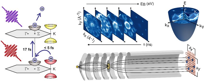
International Conference on Internal Interfaces ICII-2021

 Recent Advances in Probing Excited States at Interfaces
 by Time-resolved ARPES
 Martin Wolf
 Fritz Haber Institute of the Max Planck Society, Berlin, Germany
 Email: wolf@fhi-berlin.mpg.de

Ultrafast photoexcitation at interfaces may lead to non-equilibrium phenomena like ultrafast phase
transitions or interfacial charge and energy transfer coupled to nuclear motion. Such processes are
characterized by pronounced changes of in the electronic structure and occupation of electronic
states. Here I discuss recent advances to probe such transient changes by a table-top 500 kHz HHG
based XUV laser source enabling excited state band mapping throughout the complete Brillouin
zone by time-resolved photoemission spectroscopy (trARPES) employing a hemispherical
analyzer and a momentum microscope in the same setup [1]. Such trARPES experiments provide
detailed insights into the photo-induced phase transitions [2], the extend of the excitonic wave
function in WSe2 [3], and the ultrafast interlayer electron and energy transfer dynamics in a
monolayer-WSe2/graphene heterostructure (see figure below).

Acknowledgement: Collaboration with Shuo Dong, Samuel Beaulieu, Chris Niocholson, Tommaso Pincelli, Michele
Puppin, Julian Maklar, Laurenz Rettig and Ralph Ernstorfer
[1] M. Puppin et al., Rev. Sci. Instr. 90, 023104 & J. Makler et al., Rev. Sci. Instr. 91, 123112 (2020)
[2] C.W. Nicholson et al., Science 362, 821 & Beaulieu et al., Science Advances 7, eabd9275 (2021)
[3] S. Dong et al., Natural Science e10010 (2021)

 19
International Conference on Internal Interfaces ICII-2021

 Light MATTERs!!!
 Hrvoje Petek,1 Andi Li,1 Zehua Wang,1 Marcel Reutzel1,2
 1
 Department of Physics and Astronomy, University of Pittsburgh, Pittsburgh, Pennsylvania
 15260, USA
 2
 I. Physikalisches Institut, Georg-August-Universität Göttingen, Göttingen, Germany
 email: petek@pitt.edu

Light interacting with solid-state matter under perturbative conditions excites primarily electric
dipole transitions between k-vector dependent eigenstates of the periodic lattice potentials. A time-
periodic light potential, however, can modify the electronic band structure of a solid through
nonperturbative interactions entangling the light-matter interaction, and opening a route to tailor
material properties with light at will.
I will describe two examples: 1) It will happen at zero field strength when the complex dielectric
response function Re[ε(ω)]~0 and Im[ε(ω)] is small. This happens for ionic solids above the
longitudinal optical phonon frequency and for metals where the -ε∞(ω)~ εDrude(ω), or near the
interband absorption threshold. This epsilon near-zero (ENZ) response coincides with the
excitation of collective ion or electron responses, i.e., in case of metals, the bulk plasmon excitation.
I will describe the ENZ response of single crystalline, low-index surfaces of Ag, as measured by
ultrafast multiphoton photoemission (mPP) spectroscopy. This bulk plasmonic response of Ag is
fundamentally responsible for all plasmonic responses of silver, and yet the observed mPP spectra
fundamentally contradict significant aspects that we expect from theory.
2) I will also report the high field response of Cu(111) surface where light is sufficiently strong to
dress the electronic bands through Floquet engineering and Stark shift effects. The optical dressing
opens the way to modify quasiparticles in solids at will, where, for example, electrons can be
transformed into holes on subfemtosecond time scale. Our studies inform how light, electronic, and
atomic degrees of freedom in solids can overcome their natural performance boundaries.

 20
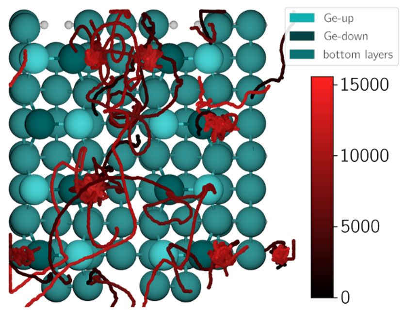
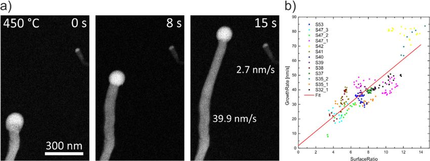
International Conference on Internal Interfaces ICII-2021

 Strongly coupled interface phonons and interface electronic
 states at lattice-matched GaP/Si(001)
 Kunie Ishioka1, Gerson Mette2, Steven Youngkin2, Andreas Beyer2,
 Christopher J. Stanton3, Wolfgang Stolz2, Kerstin Volz2, Ulrich Höfer2
 1
 National Institute for Materials Science, Tsukuba, Japan
 2
 Department of Physics, Philipps-Universität Marburg, Germany
 3
 Department of Physics, University of Florida, Gainesville, FL USA
 e-mail: ISHIOKA.Kunie@nims.go.jp

Interface of GaP and Si(001) can serve as a model semiconductor heterojunction because of the
small lattice mismatch between the two semiconductors [1]. Transient reflectivity measurements
with below-bandgap excitation of GaP with a near infrared pulse reveal a rich variety of ultrafast
phononic and electronic responses that are characteristic to the heterointerface. The polarization-
dependence of the LO phonon of the GaP layer shows a clear deviation from that of bulk GaP under
the same excitation, which is indicative of a sudden creation of charge carriers due to the ultrafast
injection from the Si substrate. In addition, the transient reflectivity of the heterointerface is also
modulated by an oscillation at 2 THz, which is not seen for the bulk semiconductors. For the GaP
nucleation layer grown at a relatively low temperature, the amplitude of this low-frequency mode
(LFM) shows a distinct peak at 1.4 eV as the excitation photon energy is swept. This resonance
behavior agrees well with that of the sub-picosecond electronic response in the same transient
reflectivity signal and in our previous second harmonic generation study [2]. These results
unambiguously demonstrate the resonant transition between the interface electronic states and the
interface phonon mode that is strongly coupled to it.

 Fig. 1 (a,b) Pump wavelength-dependence of the electronic response (a) and the interface phonon (b).
 (c) Schematic band diagram at the GaP/Si(001) interface.

[1] A. Beyer and K. Volz, Adv. Mater. Interfaces 6, 1801951 (2019).
[2] G. Mette, J. E. Zimmermann, A. Lerch, K. Brixius, J. Güdde, A. Beyer, M. Dürr, K. Volz, W. Stolz, and U.
 Höfer, Appl. Phys. Lett. 117, 081602 (2020).

 21
International Conference on Internal Interfaces ICII-2021

 Microscopic dynamics of propagating and localized
 excitations across interfaces analyzed by femtosecond solid
 state spectroscopy
 Uwe Bovensiepen
 Faculty of Physics, University of Duisburg-Essen, Germany
 e-mail: uwe.bovensiepen@uni-due.de

An excited electron propagates in condensed matter with its momentum k at an energy E(k) and
experiences elastic and inelastic scattering processes, which lead to electronic relaxation and
energy transfer to microscopic excitations of the lattice and spin systems. Experiments employing
femtosecond time-resolved photoelectron spectroscopy exploited so far very successfully the
surface sensitivity of the method and probed such scattering processes locally at or near the surface
in the time domain [1]. Here, we report on experimental results which analyze the non-local
dynamics of excited electrons in two-photon photoemission (2PPE) and demonstrate sensitivity to
buried media [2]. In these experiments one photon excites in Au/Fe/MgO(001) heterostructures
electrons in Fe. Electron propagation through the layer stack to the Au surface is detected in 2PPE
in back side pump – front side probe experiments in a time-of-flight like scheme. We observe
pronounced differences between front and back side pumping of the heterostructure which are
attributed to electron transport contributions through the layer stack. Furthermore, competition of
e-e with e-ph scattering will be discussed in [Fe/MgO]n heterostructures. Pump-probe experiments
of element specific spectroscopy in combination with electron diffraction provide here
unprecedented insights regarding the mechanism of energy transfer across interfaces and
emphasize the importance of coupling hot electrons to non-thermalized interface phonons [3].
Extension of these experimental tools to address effects of strong electron correlation [4] and spin-
dependent dynamics across interfaces [5] will be discussed.

This work was funded by the Deutsche Forschungsgemeinschaft through the Collaborative
Research Center CRC 1242.

[1] U. Bovensiepen, H. Petek, M. Wolf, Dynamics at Solid State Surface and Interfaces,
 Vol. 1, Wiley-VCH, 2010.
[2] Y. Beyazit J. Beckord, P. Zhou, J. Meyburg, F. Kühne, D. Diesing, M. Ligges, U. Bovensiepen,
 Phys. Rev. Lett. 125, 076803 (2020).
[3] N. Rothenbach, M. E. Gruner, K. Ollefs, C. Schmitz-Antoniak, S. Salamon, P. Zhou, R. Li, M. Mo, S. Park, X.
 Shen, S. Weathersby, J. Yang, X. J. Wang, R. Pentcheva, H. Wende, U. Bovensiepen, K. Sokolowski-Tinten, A.
 Eschenlohr, Phys. Rev. B 100, 174301 (2019).
[4] M. Ligges, I. Avigo, D. Golez, H. U. R. Strand, Y. Beyazit, K. Hanff, F. Diekmann, L. Stojchevska, M. Kalläne,
 K. Rossnagel, M. Eckstein, P. Werner, U. Bovensiepen,
 Phys. Rev. Lett. 120, 166401 (2018).
[5] J. Chen, U. Bovensiepen, A. Eschenlohr, T. Müller, P. Elliott, E. K. U. Gross, J. K. Dewhurst,
 S. Sharma, Phys. Rev. Lett. 122, 067202 (2019).

 22
International Conference on Internal Interfaces ICII-2021 Electronic Properties of Interfaces with N-Heteropolycyclic Molecules Petra Tegeder Physikalisch-Chemisches Institut, Ruprecht-Karls-Universität Heidelberg, Germany e-mail: tegeder@uni-heidelberg.de For improvement and optimization of the performance of organic molecule-based devices, such as photovoltaic cells and thin-film transistors comprehensive insight into the physical and chemical properties of the organic molecules at surfaces is necessary. N-heteropolycyclic aromatic compounds are promising candidates for n-channel semiconductors. The introduction of nitrogen atoms into the -backbone of the polycyclic aromatic hydrocarbons stabilizes the frontier orbitals and increases the electron affinity, while the size of the HOMO−LUMO (optical) gap is nearly unaffected. By using two-photon photoemission spectroscopy (2PPE) and high resolution electron energy loss spectroscopy (HREELS) we determined quantitatively transport, singlet and triplet states as well as electronic spectra of serval N-heteropolycyclic molecules adsorbed on Au(111) [1-5]. Using angle-resolved 2PPE we identified strongly dispersing occupied and unoccupied electronic states, which result from hybridization between localized molecular states and delocalized metal bands at the metal/organic interface [4, 5]. We acknowledge funding by the German Research Foundation through the SFB 1249 (N- Heteropolycycles as Functional Materials) and the Cluster of Excellence (3D Matter Made to Order). [1] M. Ajdari, T. Schmitt, M. Hoffmann, F. Maaß, H. Reiss, U. H. F. Bunz, A. Dreuw, P. Tegeder, J. Phys. Chem. C 124 (2020) 13196. [2] M. Ajdari, A. Stein, M. Hoffmann, M. Müller, U. H. F. Bunz, A. Dreuw, P. Tegeder, J. Phys. Chem. C 124 (2020) 7196. [3] M. Ajdari, F. Landwehr, M. Hoffmann, H. Hoffmann, U. H. F. Bunz, A. Dreuw, P. Tegeder, J. Phys. Chem. C 125 (2021) 6359. [4] A. Stein, D. Rolf, C. Lotze, B. Günther, L. H. Gade, K. J. Franke, P. Tegeder, J. Phys. Chem. Lett. 12 (2021) 947. [5] A. Stein, D. Rolf, C. Lotze, S. Feldmann, D. Gerbert, B. Günther, A. Jeindl, J.J. Cartus, O.T. Hofmann, L.H. Gade, K.J. Franke, P. Tegeder, J. Phys. Chem. C 125 (2021) 19969. 23
International Conference on Internal Interfaces ICII-2021

 Quantifying ultrafast energy dissipation pathways in
exfoliated and stacked van der Waals materials with energy-,
 momentum-, and time-resolution
 Marcel Reutzel, Marius Keunecke, David Schmitt, Jan Philipp Bange, Wiebke Bennecke,
 Marco Merboldt, Marten Düvel, Daniel Steil, G. S. Matthijs Jansen, Sabine Steil,
 Stefan Mathias
 I. Physikalisches Institut, Georg-August-Universität Göttingen, Germany
 e-mail: marcel.reutzel@phys.uni-goettingen.de

The atomic thickness and large chemical variety of two-dimensional van der Waals materials make
them an exciting playground to investigate and control energy conversion processes on the atomic
scale. The full potential of these materials can be exploited by stacking them into three-dimensional
architectures: the (opto-)electronic material properties are then not only defined by the separate
material sheets, but by the interlayer coupling and the respective Moiré potential, which can be
manipulated by the relative momentum mismatch of the monolayer sheets. In order to explore the
response of such material systems to an optical excitation, typically, time-resolved all-optical
spectroscopies are employed. However, such experiments lack information on the momentum of
the charge carriers involved, which is crucial for a detailed quantification of ultrafast energy
dissipation pathways.
In this contribution, we will describe our efforts to quantify the ultrafast carrier dynamics in
exfoliated and stacked van der Waals materials with complete energy-, momentum-, and time-
resolution. First, we will introduce our new time-resolved photoemission experiment that combines
a 1 MHz table-top extreme ultraviolet light source with a time-of-flight momentum microscope
[1]. Second, we will describe the excited charge carrier dynamics of epitaxial graphene and in doing
so pinpoint the contribution of distinct e-e and e-p scattering pathways to the overall dynamics [2].
Finally, we will discuss our efforts to probe exfoliated and stacked van der Waals materials in the
time-resolved momentum microscopy experiment [Fig. 1].

Fig. 1.: Time-resolved momentum microscopy on exfoliated monolayer graphene. (a) Energy- and momentum-
resolved photoemission spectra are selectively collected from few µm sized sample areas by placing an aperture into
the image plane of the microscope. Either the energy filtered (b) real or (b) momentum space image is projected onto
the detector.

[1] Keunecke et al., Rev. Sci. Ins. 91, 063905 (2020).
[2] Keunecke et al., arXiv:2012.01256 (2020).

 24
International Conference on Internal Interfaces ICII-2021

 Oral Abstracts Tuesday

 25
International Conference on Internal Interfaces ICII-2021

 26
International Conference on Internal Interfaces ICII-2021

 Different reaction mechanisms of two biphenyl-based
 molecules on Ag(111) surface
 Zhiwen Zeng, Lin Feng, Tao Wang, Junfa Zhu*
National Synchrotron Radiation Laboratory and Department of Chemical Physics, University of
 Science and Technology of China, Hefei, 230029, P. R. China
 e-mail: jfzhu@ustc.edu.cn

On-surface synthesis (OSS) has shown its great potential in the fabrication low-dimensional
covalent nanostructures with atomic precision in the last decade.1 To obtain the high-quality
covalent nanostructures, there is a need for a greater understanding of the underlying mechanisms
of OSS. Here, we report an example that demonstrates the clear interdependence between surface-
supported reactions and molecular adsorption configurations. Two biphenyl-based molecules with
two and four bromine substituents, i.e. 2,2’-dibromo-biphenyl (DBBP) and 2,2’,6,6’-tetrabromo-
1,1'-biphenyl (TBBP), show completely different reaction pathways on a Ag(111) surface, leading
to the selective formation of dibenzo[e,l]pyrene and biphenylene dimer, respectively.2 By
combining low-temperature scanning tunneling microscopy, synchrotron radiation photoemission
spectroscopy, and density functional theory calculations, we unravel the underlying reaction
mechanism. After debromination, a bi-radical biphenyl can be stabilized by surface Ag adatoms,
while a four-radical biphenyl undergoes spontaneous intramolecular annulation due to its extreme
instability on Ag(111). Such different chemisorption-induced precursor states between DBBP and
TBBP consequently lead to different reaction pathways after further annealing. The precise
regioselective aryl-aryl coupling will reduce the flexibility of the DBBP which lead to the
formation of planar dibenzo[e,l]pyrene (DB[e,l]P) via hierarchical intermolecular aryl-aryl
coupling and cyclodehydrogenation. In contrast, the high selectivity toward a biphenylene dimer
is attributed to the special adsorption configuration of TBBP on Ag(111).

 Fig. 1 Reaction pathways of (a) DBBP and (b) TBBP on the Ag(111) surfaces, respectively.

[1] T. Wang, J.F.Zhu, Confined On-Surface Organic Synthesis: Strategies and Mechanisms. Surf. Sci. Rep. 74, 97
 (2019).
[2] L. Feng, et al., On-Surface Synthesis of Planar Acenes via Regioselective Aryl-Aryl Coupling. Chem. Commun.
 56, 4890 (2020).

 27
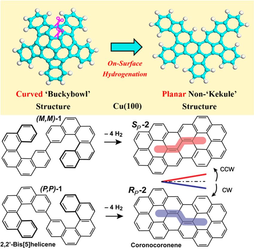
International Conference on Internal Interfaces ICII-2021

 Planarization of non-planar aromatic hydrocarbons:
 Dehydrogenation versus hydrogenation
 Karl-Heinz Ernst1,2,3
 1
 Empa, Swiss Federal Laboratories for Materials Science and Technology, Switzerland
 2
 Department of Chemistry, Universität of Zurich, Switzerland
 3
 Institute of Physics, Czech Academy of Sciences, Prague, Czech Republik
 e-mail: karl-heinz.ernst@empa.ch

Besides their interest for potential organic electronic devices, modification of polycyclic aromatic
hydrocarbons (PAH) on surfaces is believed to play a role in new organic electronic devices, light
sensors or for electron-spin filters. We will present different aspects of modification of various
single crystal metal surfaces in ultrahigh vacuum with PAHs, such as carbohelicenes and
buckybowls.
The buckybowl pentaindenocorannulene adsorbs on a Cu(100) surface in two different modes,
namely, bowl cavity up and bowl cavity down [1,2]. The latter dehydrogenates and delivers the
hydrogen for hydrogenation of the cavity-up species. Cleavage of C-C bonds in two steps leads to
a planar PAH with surface-quenched open shell character (Fig. 1, top). Cyclodehydrogenation of
2,2’-bispentahelicene, on the other hand, proceeds stereospecifically to coronocoronene, which is
chiral due to surface confinement (Fig. 1, bottom) [3]. The role of steps, adatoms and vacancies in
these processes will be discussed.

 Fig. 1. Two examples in which planarization occurs by
 hydrogenation and C-C bond cleavage or by
 dehydrogenation and C-C bond coupling.

[1] L. Li et al. ACS Nano 15, 3578 (2021).
[2] Wäckerlin et al. ACS Nano 14, 16735 (2020).
[3] B. Irziqat, A. Cebrat et al. Chemistry-Eur. J. doi.org/10.1002/chem.202102069

 28
International Conference on Internal Interfaces ICII-2021

 Carbon Nanostructures from On-Surface Synthesis
 Qitang Fan1, Linghao Yan2, Qigang Zhong3, Jose Martinez-Castro4, Anja Haags4, Daniel
 Martin-Jimenez3, Daniel Ebeling3, Matthias W. Tripp1, Ondřej Krejčí2, Stefan R. Kachel1,
 Adam S. Foster2, Ulrich Koert1, Serguei Soubatch4, F. Stefan Tautz4, André Schirmeisen3,
 Peter Liljeroth2, J. Michael Gottfried1
 1
 Department of Chemistry, Philipps-Universität Marburg, Hans-Meerwein-Straße 4, 35032
 Marburg, Germany
 2
 Department of Applied Physics, Aalto University, FI-00076 Aalto, Finland
 3
 Institute of Applied Physics (IAP), Justus Liebig University Gießen, Heinrich-Buff-Ring 16,
 35392 Gießen, Germany
 4
 Peter Grünberg Institut (PGI-3), Forschungszentrum Jülich, 52425 Jülich, Germany.
 e-mail: qitang.fan@uni-marburg.de

In recent years, reactions at solid surfaces have been found extremely promising for the synthesis
of planar carbon nanostructures, e.g., nanographenes, graphene nanoribbons, and nanoporous
graphene [1]. The quest for planar carbon nanostructures with novel topologies persistently
intrigues scientists because of their potentially remarkable properties. Here, by using custom
designed organic precursors, we show the on-surface synthesis of carbon nanostructures with
special topologies, including graphene nanorings, porous graphene nanoribbon, and nonbenzenoid
graphene isomers (e.g., biphenylene sheet [2] in Fig. 1). Their electronic properties were studied
with scanning tunneling spectroscopy and photoemission spectroscopy. The novel hierarchical on-
surface reactions developed therein are expected to enrich the bottom-up toolbox for the synthesis
of other theoretically proposed carbon nanostructures with exotic properties [3].

 Fig. 1 Structural model of a new carbon allotrope: biphenylene sheet [2].

[1] L. Talirz, P. Ruffieux, R. Fasel, Adv. Mater. 28, 6222-6231 (2016).
[2] Q.T. Fan et al., Science 372, 852-856 (2021).
[3] S. Clair, D. G. de Oteyza, Chem. Rev. 119, 4717-4776 (2019).

 29
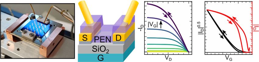
International Conference on Internal Interfaces ICII-2021

 Cyclooctynes on Si(001): A synthetic chemist’s perspective
 M. Reutzel1, M. A. Lipponer1, T. Glaser3, C. Länger3, L. Freund3, N. Münster2, P.
 Nikodemiak,2 J. Meinecke2, U. Höfer,1 U. Koert2, M. Dürr3
 1
 Department of Physics, Philipps-Universität Marburg, Germany
 2
 Department of Chemistry, Philipps-Universität Marburg, Germany
 3
 Institute of Applied Physics, Justus-Liebig-Universität Gießen, Germany
 e-mail: koert@chemie.uni-marburg.de

The predictable synthesis of structurally defined interfaces is an important goal to regulate their
physical, electronic, photophysical, and chemical properties. Here, progress towards the layer-by-
layer synthesis of organic/semiconductor interfaces is reported. Functionalized cyclooctynes show
a chemoselective reaction of the strained alkyne with the Si(001) surface. The achieved selectivity
originates from a direct adsorption pathway of cyclooctyne as opposed to the majority of other
organic functionalities. A layer-by layer synthesis can be achieved by combination of UHV-physics
and solution chemistry.[1] Alternatively, an UHV-only strategy is possible using 4+2 cycloadditions
with inverse electron demand and strain-promoted azide/cyclooctyne 3+2 cycloadditions.[2]

 Fig. 1: UHV-only strategy using 4+2 cycloadditions with inverse electron demand and azide/cyclooctyne 3+2
 cycloadditions.

[1] T. Glaser, J. Meinecke, C. Länger, J. Hepp, UK, M. Dürr, J. Phys Chem C 2021, 125, 4021
[2] T. Glaser, J. Meinecke, L. Freund, C. Länger, J. N. Luy, R. Tonner, UK, M. Dürr, Chem. Eur. J. 2021, 27, 8082.

 30
International Conference on Internal Interfaces ICII-2021

 Engineering of Printable and Air-Stable Silver Electrodes
 with High Work Function using Contact Primer Layer:
 From Organometallic Interphases to Sharp Interfaces
 F. Widdascheck, D. Bischof, G. Witte
 Department of Physics, Philipps-University Marburg, Germany
 e-mail: gregor.witte@physik.uni-marburg.de

Contact engineering is an important issue for organic electronics as it allows to reduce charge
carrier injection barriers. While the use of molecular contact primer layers to control the energy
level alignment is demonstrated in many concept studies mainly using (single crystalline) model
substrates, the processability of electrodes, and their robustness (e.g., to air exposure) must also be
considered in real devices. Although silver electrodes can be printed using silver ink, their low
work function and sensitivity to oxidation severely limits their use for printable organic electronics.
The present work demonstrates that contact primer monolayers of F4TCNQ and F6TCNNQ allow
to meet these requirements and provide a reliable approach to engineer high work function silver
electrodes, which is examined for Ag(111) as well as polycrystalline and silver ink substrates.
Notably, upon multilayer growth of these organic acceptor films, a pronounced intercalation of
silver into the molecular adlayer occurs at room temperature yielding an organometal interphase
extending over the entire adlayer, which is stabilized by a charge transfer from the metal. It is
shown that heating allows controlled desorption of this interphase leaving behind a well-defined
monolayer that is further stabilized by an additional charge transfer into the acceptor molecules
and causes a complete filling of the former LUMOs. Especially F6TCNNQ contact primer layers
can also be prepared on oxidized silver electrodes and reliably yield work functions of 5.5–5.6 eV,
which can even withstand air exposure. In addition, such contact primers show no interdiffusion
into subsequently deposited layers of the prototypical p-type organic semiconductor pentacene,
hence validating their use for organic electronic devices [1].

Fig. 1 Schematic summary of the structure and thermal stability of F6TCNNQ films on silver electrodes.

[1] F. Widdascheck, D. Bischof, G. Witte. Adv. Funct. Mater. 10.1002/adfm.202106687 (2021).

 31
International Conference on Internal Interfaces ICII-2021

 Step-directed alignment of epitaxial transition metal
 dichalcogenide monolayers on sapphire
 Haoyue Zhu1, Tanushree H. Choudhury1, Nicholas Trainor2, Thomas V. McKnight2,
 Anushka Bansal2 and Joan M. Redwing1,2
 1
 2D Crystal Consortium, 2Dept. of Materials Science and Engineering
 The Pennsylvania State University, University Park, PA USA
 e-mail: jmr31@psu.edu

Transition metal dichalcogenides (TMDs) form a compelling class of 2D materials with potential
applications in optoelectronics, flexible electronics, chemical sensing and quantum technologies.
At the monolayer limit, the semiconducting TMDs (e.g., MX2 where M = Mo/W and X = S/Se)
exhibit direct band gaps within the visible range, large exciton binding energies and spin-valley
polarization. The lack of out-of-plane bonding on the van der Waals surface of these materials
enables heterostructure formation without the constraints of lattice matching.
Wafer-scale synthesis of semiconducting TMD monolayers is of significant interest for device
applications. Promising results have been demonstrated for epitaxial films deposited by vapor
phase techniques such as chemical vapor deposition (CVD) and metalorganic CVD (MOCVD).
However, the three-fold symmetry of TMDs such as MoS2 and WSe2, typically results in two
energetically equivalent domain alignments, often referred to as 0o and 60o domains, when grown
on substrates such as c-plane sapphire and graphene. The oppositely oriented domains give rise to
inversion domain boundaries upon coalescence which exhibit a metallic character.
In this study, we demonstrate the epitaxial growth of unidirectional TMD monolayers by MOCVD
on 2” diameter c-plane sapphire substrates with a significantly reduced density of inversion
domains [1]. Steps on the sapphire surface are shown to break the surface symmetry giving rise to
a preferred domain orientation. The as-received sapphire substrates, which are miscut ~0.2o toward
, consist of steps with sub-1 nm step height separated by 50-70 nm wide terraces. A three-
step nucleation-ripening-lateral growth process, carried out at temperatures ranging from 850oC to
1000oC, was used to achieve epitaxial films of WSe2 and WS2 using W(CO)6, H2Se and H2S as
precursors in a H2 carrier gas [2]. Nucleation was observed to occur at the step edge and the growing
domains align epitaxially with the underlying (0001) sapphire lattice. As a result of the nucleation
process, the domains grow with a zig-zag edge facing the top terrace edge which imparts a
preferential direction to the domains. The percentage of domains with a preferred direction ranges
from 75%-86% depending on MOCVD growth conditions. Continued lateral growth for times
ranging from 10-30 minutes results in fully coalesced TMD monolayers that are epitaxially oriented
on the sapphire, as assessed by in-plane x-ray diffraction, with a reduced density of inversion
domain boundaries. The results demonstrate the important role of surface structure in nucleation
and epitaxial growth of TMD monolayers.
[1] M. Chubarov et al., ACS Nano 15, 2532-2541 (2021).
[2] X. Zhang et al., Nano Lett. 18, 1049-1056 (2018).

 32
International Conference on Internal Interfaces ICII-2021

 Interfacial Interactions at Hybrid Organic / Layered
 Materials Interfaces
 Oliver L.A. Monti1,2
 1
 Department of Chemistry and Biochemistry, University of Arizona, USA
 2
 Department of Physics, University of Arizona, USA
 e-mail: monti@u.arizona.edu

Van der Waals layered materials offer an unprecedented sandbox for designing and probing
quantum materials and strongly correlated materials. This is in large part due to their ease of
fabrication and assembly into complex heterostructures with broadly tunable properties. Despite
these unique advantages, the scope of functionalities and new physics of van der Waals layered
materials has the potential to be enhanced even further if heterostructures beyond the layered
materials are explored. Organic semiconductors are particularly advantageous in this context: They
can be designed and synthesized essentially at will, and their internal interfaces reveal striking new
properties that go beyond the organic materials on their own.

Here I will discuss two case studies where we investigate the new physics that arises at the interface
of a layered materials and an organic semiconductor: I will show how the combination with
carefully tailored organic semiconductors leads to the emergence of spin texture in a topological
insulator [1], and how the combination of 2D materials and organic semiconductors creates hybrid
excitons and strong Raman enhancement [2]. These two examples are showcases of the power of
combining atomically hybrid heterostructures.

[1] S. Jakobs et al., Nano Lett. 15, 6022 (2015).
[2] C. Muccianti et al., J. Phys. Chem. C 124, 18302 (2020)

 33
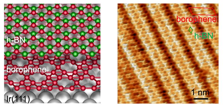
International Conference on Internal Interfaces ICII-2021

 Borophenes made easy: Distinct polymorphs and
 heterostructures
 Marc G. Cuxart1, Knud Seufert1, Valeria Chesnyak1, Wajahat A. Waqas1, Anton Robert2,
 Marie-Laure Bocquet2, Georg S. Duesberg3, Hermann Sachdev3, Willi Auwärter1
 1
 Physics Department E20, Technical University of Munich, Germany
 2
 Département de Chimie, Ecole Normale Supérieure, France
 3
 Fakultät für Elektrotechnik und Informationstechnik, Universität der Bundeswehr München,
 Germany
 e-mail: wau@tum.de

Surface-supported two-dimensional (2D) materials keep attracting considerable interest. For
example, borophene, a synthetic, boron-based 2D material, offers intriguing anisotropic electronic
and mechanical properties [1,2]. Here, we present a versatile chemical vapor deposition (CVD)
approach to grow atomically-thin 2D polymorphs of borophene by using diborane. This precursor
originates from byproducts of commercial borazine, a popular material for growth of hexagonal
boron nitride (h-BN). Specifically, borophene polymorphs with large single-crystalline domains
are synthesized on Cu(111) and Ir(111) supports. Additionally, atomically-precise lateral interfaces
or vertical van der Waals heterostructures combining borophene and h-BN can be achieved by
sequentially dosing different precursors from the same supply (Fig. 1). Thereby, borophene is
protected from immediate oxidation by a single h-BN overlayer. The borophene polymorphs and
interfaces with h-BN are comprehensively characterized by low-temperature scanning tunneling
microscopy and spectroscopy, x-ray photoelectron spectroscopy, and complementary density
functional theory modeling. The ability to synthesize high-quality borophenes by a straight-
forward, scalable CVD approach opens up opportunities for the study of their fundamental
properties and for device incorporation.

Fig. 1. Scheme (left panel) and atomically-resolved STM image (right panel) of a vertical heterostructure with h-BN
 covering borophene on Ir(111).

[1] A.J. Mannix et al., Nat. Rev. Chem. 1, 1 (2017).
[2] P. Ranjan et al., Adv. Mater. 32, 2000531 (2020).

 34
International Conference on Internal Interfaces ICII-2021

 Oral Abstracts Wednesday

 35
International Conference on Internal Interfaces ICII-2021

 36
International Conference on Internal Interfaces ICII-2021

 Manipulating quantum states by photoexcitation in two
 dimensional
 Sheng Meng
 Institute of Physics, Chinese Academy of Sciences, Beijing 100190, China
 e-mail: smeng@iphy.ac.cn

Photoexcitation is a powerful means in distinguishing different interactions and manipulating the
states of matter, especially in complex quantum systems. Here we demonstrate photoexcitation
induced ultrafast dynamics in two-dimensional quantum materials using time-dependent density
functional theory molecular dynamics. In particular, we discover a novel mechanism which
involves self-amplified exciton-phonon dynamics for the formation of charge density wave
(CDW), and we predict a new collective mode induced by photoexcitation which is significantly
different from thermally-induced phonon mode. We will also discuss photoinduced electronic
phases in other two-dimensional materials such as controlling the dynamics of Weyl quasiparticles
in semimetal WTe2 (Fig. 1). Our results provide insights from a new perspective on the coherent
electron and lattice quantum dynamics in materials upon photoexcitation.

 Figure 1. The dynamics of Weyl points distribution in response to different photoexcitation.

[1] M.X. Guan, E. Wang, P.W. You, J.T. Sun, S. Meng. Manipulating Weyl quasiparticles by orbital-selective
 photoexcitation in WTe2. Nature Commun. 12, 1885 (2021).
[2] H. Lakhotia, H.Y. Kim, M. Zhan, S.Q. Hu, S. Meng, E. Goulielmakis. Laser picoscopy of valence electrons in
 solids. Nature 583, 55 (2020).
[3] C. Lian, S.J. Zhang, S.Q. Hu, M.X. Guan, S. Meng. Ultrafast charge ordering by self-amplied exciton-phonon
 dynamics in TiSe2. Nature Commun. 11, 43 (2020).

 37
International Conference on Internal Interfaces ICII-2021

 Excitons in atomically thin 2D semiconductors
 Xavier Marie
Université de Toulouse, INSA-CNRS-UPS, Laboratoire de Physique et Chimie des Nano-Objets,
 135 Avenue de Rangueil, 31077 Toulouse, France
 e-mail: marie@insa-toulouse.fr

In this talk I will first recall the general properties of 2D excitons in Transition Metal
Dichalcogenides monolayers: giant binding energy, oscillator strength, exchange interactions,
spin/valley…
Encapsulation of monolayers such as MoSe2 in hexagonal boron nitride (hBN) yields narrow
optical transitions approaching the homogeneous exciton linewidth [1,2]. We demonstrate that the
exciton radiative rate in these van der Waals heterostructures can be tailored by a simple change of
the hBN encapsulation layer thickness [3].
We also measured the exciton fine structure of MoS2 and MoSe2 monolayers encapsulated in boron
nitride by magneto-photoluminescence spectroscopy in magnetic fields up to 30 T [4,5].
Finally I will present recent optical spectroscopy experiments on the control of interlayer excitons
in MoS2 bilayers [6,7]. We show that there is a correlation between the stacking order and the
interlayer coupling of valence states in both as-grown MoS2 homobilayer samples and in artificially
stacked bilayers from monolayers. We also evidenced a giant Stark splitting of the interlayer
excitons characterized by a large oscillator strength in bilayer MoS2.

[1] F. Cadiz et al, Phys. Rev. X 7, 021026 (2017)
[2] G. Wang et al, Phys. Rev. Lett. 119, 047401 (2017)
[3] H. Fang et al, Phys. Rev. Lett 123, 067401 (2019)
[4] C. Robert et al, Phys. Rev. Lett . 126, 067403 (2021)
[5] C. Robert et al, Nature Com. 11, 4037 (2020)
[6] I. Paradisanos et al, Nature Com. 11, 2391 (2020)
[7] N. Leisgang et al, Nature Nano. 15, 901 (2020)

 38
International Conference on Internal Interfaces ICII-2021

 Revealing the structure and orientation of organic
 nanocrystallites in bulk heterojunction solar cells using 4D
 Scanning Confocal Electron Diffraction (4D-SCED)
 Mingjian Wu1, Christina Harreiss1, Erdmann Spiecker1
 1
 Institute of Micro- and Nanostructure Research & Center for Nanoanalysis and Electron
 Microscopy (CENEM), Universität Erlangen‐Nürnberg
 e-mail: erdmann.spiecker@fau.de

The performance of bulk heterojunction (BHJ) organic solar cells is dictated by the
nanomorphology and crystallinity of the organic blend, including size and orientation of (donor)
nanocrystallites, donor-acceptor interfaces, and degree of percolation, which determine the
efficiency of exciton dissociation and charge carrier transport. However, revealing the nanoscale
structures at high spatial resolution using electron microscopy is challenged by radiation sensitivity
of the organic materials. Nanobeam diffraction (NBD) imaging, also known as 4D-STEM, has
recently emerged and demonstrated to map the orientation and study π-stacking structures in
organic semiconductors molecular crystals, opening a new application field in beam sensitive soft
materials [1]. In 4D-STEM, pixelated detectors are used to record the full 2D diffraction pattern at
each probed sample position, allowing reciprocal space details of the scattered intensities to be
analyzed afterwards. However, the NBD mode is intrinsically not optimized for dose efficiency as
(i) a focused probe is interacting with a small sample region (high dose rate) and (ii) the far field
diffraction disks are detected spreading over many pixels of the detector/camera, resulting in low
signal to noise ratio (SNR). Moreover, for molecular crystals with relatively large unit cell
parameters disk overlap severely limits the angular resolution of the technique.
Here, we propose a novel 4D-STEM modality based on a
scanning confocal electron diffraction (SCED) setup, which
combines high angular resolution with high contrast and low
dose [2]. We use the 4D-SCED method to study the
structure and orientation of molecular nano-crystallites in
DRCN5T:PC71BM BHJ thin films. We show its high
angular resolution for investigating the rich structural
information of the molecular crystals, and demonstrate that
this 4D-STEM modality is capable to improve dose
efficiency by about one order of magnitude at identical dose
budget compared to standard NBD setup. We furthermore
show that 4D-SCED can even be used to monitor the growth
 Fig. 1 Visualization of the orientation of edge-on
and structural evolution of the nanocrystallites in situ during DRCN5T donor nano-crystallites (colored) and
annealing at elevated temperatures. distribution of face-on grains (gray) from 4D-
 SCED. Scale bars: 500 nm (left), 2 mrad (right).

[1] O. Panova et al., Nature Materials, 18, 860-865 (2019).
[2] M. Wu et al., Microsc. Microanal., 27(S1), 194-197 (2021). doi:10.1017/S1431927621001306

 39
International Conference on Internal Interfaces ICII-2021

 Chemical reactivity and electronic correlations
 in 2D-materials tuned by internal interfaces
 Thomas Michely
 II. Physikalisches Institut, Universität zu Köln, Germany
 e-mail: michely@ph2.uni-koeln.de

Two dimensional materials are atomically thin and display a front- and a backside. Through
interface interaction with a layer of atoms, another 2D layer, or a bulk substrate on its backside, the
2D layer electronic properties and its frontside interaction with the environment are largely
changed.
Doping of graphene through intercalation layers on its backside changes the ionic binding of
adsorbates to graphene, graphene’s van der Waals interaction with organic molecules and even
reaction pathways in organo-metallic synthesis on its frontside.
Doping graphene itself can also be used for non-invasive chemical gating of 2D layers placed on
top. For MoS2 grown on doped and un-doped graphene on Ir(111) we demonstrate shifts of the
band structure by up to 1.1 eV, severe band gap renormalization, and an insulator-to-metal
transition.
Thereby it is also possible to manipulate 1D internal interface states in MoS2, e.g. the 1D electronic
states in mirror twin boundaries. One fundamental consequence of the analysis of 1D band filling
and bending is the confirmation of a long standing theoretical prediction for the quantized
polarization charge on mirror twin boundaries.

 40
You can also read