Josephson dynamical simulation using the electronic circuit simulator APLAC: a tutorial
←
→
Page content transcription
If your browser does not render page correctly, please read the page content below
Josephson dynamical simulation using the electronic circuit
                                                                   simulator APLAC: a tutorial
                                                                                             Mikko Kiviranta
arXiv:2103.11465v1 [cond-mat.supr-con] 21 Mar 2021

                                                                                                  Abstract
                                                              Analysis Program for Linear Active Circuits (APLAC) is a general-purpose electronic
                                                          circuit simulator, which has included a built-in model of the Josephson junction (JJ) since
                                                          late 80’s. It capabilities in simulating eg. noisy Superconducting Quantum Interference
                                                          Devices (SQUIDs), Rapid Single Flux Quantum (RSFQ) logic circuits, or superconducting
                                                          Transition Edge Sensors (TESes) are relatively unknown within the superconducting elec-
                                                          tronics community. Here we give a brief step-to-step tutorial for APLAC users to unleash
                                                          those capabilities.

                                                     1    Introduction
                                                     APLAC is a general-purpose electronic circuit simulator whose humble beginnings [1, 2], are
                                                     almost as old as the much more widely-known SPICE simulator. Josephson junction was available
                                                     already in its early versions, at least from the version 6.24 which the author learned to use in the
                                                     early 90’s. Such functionality has been useful and continues to be useful in designing Josephson
                                                     devices, including SQUIDs and SQUID arrays with parasitics. APLAC is a contemporary of a
                                                     number of other JJ-equipped simulators including the WR-SPICE [3] and JSIM [4], but less well
                                                     known.
                                                         A lot of effort went into development of APLAC after Nokia Corporation began using it
                                                     as their major microwave design tool. The NASSE schematic editor was developed along with
                                                     the originally text-based APLAC simulation engine. The APLAC version 6.24 (maybe already
                                                     earlier) included the integrated schematic capture, which feature made the APLAC attractive for
                                                     Josephson dynamical simulations involving parasitics. Our earlier, hand-written code (eg. [5, 6])
                                                     had to be re-written and re-compiled whenever circuit topology (i.e. schematics) changed. The
                                                     6.24 was a 16-bit application in Windows, so that memory limitations prevented long simulation
                                                     runs. From the version 7.10 onwards the simulator was a 32-bit Windows application, wich
                                                     together with the rapidly increasing processor speeds made Josephson simulations feasible even
                                                     in this kind of an intepreted rather than compiled form.
                                                         The spin-off company APLAC Inc was established to sell and further develop the simulator
                                                     as stand-alone software, but in 2005 the company was acquired by Applied Wave Research and
                                                     APLAC got merged into their Microwave Office suite. More recently, APLAC has been acquired
                                                     along with the AWR by the Cadence Design Systems.
                                                         This document is intended as a companion to the paper ’Superconductive circuits and the
                                                     general-purpose electronic simulator APLAC’ accepted to IEEE Transactions on Applied Super-
                                                     conductivity, and to act as a wrapper to the relevant simulation code files. This tutorial was
                                                     originally located as a web page.

                                                                                                      1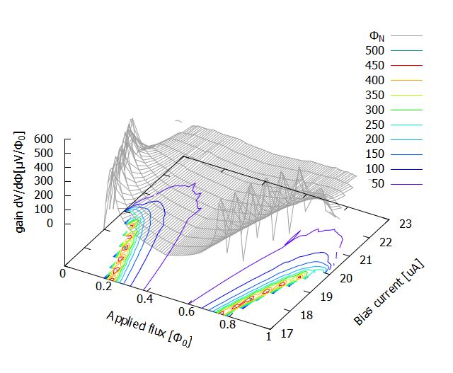
Figure 1: Josephson junction modelled by LT-SPICE IV

1.1    Josephson junction model using controlled sources: LT-SPICE
It is straighforward to use a controlled current source to realize the first Josephson relation,
I(t) = IC sin(2π θ(t)) and to re-intepret a voltage of an internal node to present the quantum
                  Rt
phase θ(t) = Φ10 0 U (τ ) dτ . Quantum phase can then be generated by an integrator driven by
the instantaneous voltage across the J-junction. Most straighforward an integrator is a controlled
current source charging a capacitor.
    Shown in Fig.1 is a resistively shunted J-junction implemented in the LT-SPICE version IV,
with the schematic JJ2.asc available as an ancilliary file. The J-junction model with IC = 100µA
is driven here by a bias source ramping the current up to JC = 0 . . . 120µA in 100 nanoseconds.
The .tran directs recording of the final 20 nanoseconds of voltage across B2, which corresponds
the IB = 96µA . . . 120µA. The record shows the onset and increasing frequency of the Josephson
oscillation as the bias current exceeds IC .
    A full dc-SQUID can be constructed from such J-junctions as shown in Fig.2 (LT-SPICE
schematic SQ2.asc available as ancilliary). In the simulation the first 2ns are used to ramp up
the SQUID bias current IB = 0 . . . 20.1µA , so that IB > 2IC makes the SQUID remain in
the finite-voltage state at all flux values. The applied flux is driven over 2 flux quanta, 2Φ0 ,
during the 100ns total simulation time. The low-pass filter R3/C3 averages out the Josephson
oscillation, so that the flux-to-voltage response of the SQUID gets plotted as the voltage across
C3.

1.2    Josephson junction model using controlled sources: APLAC
With APLAC, the same circuits can be constructed from voltage-controlled current sources
(VCCS’s) as shown in Fig.3. Simulating from the schematic JJ2.N and netlist JJ2.I, available
as ancilliary files, similar time behaviour follows.
    The APLAC version of the dc-SQUID is described in the schematic SQ2.N and the SQ2.I
netlist, available as ancilliary files. The simulation result is shown in Fig. 4.
    In APLAC, however, there exists the Josephson junction as a built-in library element. The
circuits are much more convenient to construct and simulate faster with the library element. The

                                                2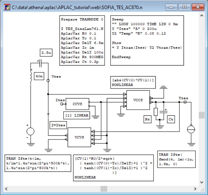
Figure 2: DC-SQUID modelled by LT-SPICE IV

                    3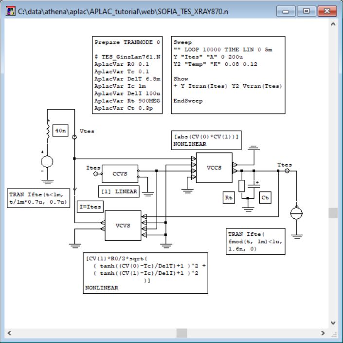
Figure 3: Josephson junction modelled by APLAC controlled sources

   Figure 4: DC-SQUID modelled by APLAC controlled sources

                               4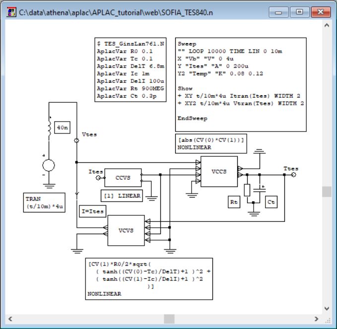
Figure 5: Simulating with the built-in JJ in APLAC

                Figure 6: DC-SQUID constructed from built-in JJs in APLAC

basic J-junction can be demonstrated with the schematic JJ3.N and netlist JJ3.I available as
ancilliary. The result is the same as by using controlled sources, as seen in the Fig.5.
    Similarly, the DC-SQUID construction becomes simpler (schematic SQ3.N and netlist SQ3.I
as ancillary), see Fig. 6.

2    Noisy SQUID simulated in APLAC
It is straightforward to build a time domain simulation of a dc-SQUID using the built-in JJ
element. In superconducting circuits the Kirchoffs voltage law is modified: not only voltages
around any closed loop vanish, but also time integrals of voltages (i.e. fluxes) around any closed
loop vanish. (More precisely, they do not vanish but are multiples of the flux quantum Φ0 -
this is enforced in simulation if there is a J-junction breaking the loop). To make the APLAC
calculate the initial condition correctly, the simulation must start at zero initial currents and
voltages, and must be driven into the setpoint explicitly.
    Often, SQUID simulations are performed in dimensionless variables. Here we use SI units
for voltages and currents, and realistic values for SQUID parameters. After a simulation run is
performed with a given set of SI dimensions, the dimensionless variables [8] tell how the results
scale into some other set of SI dimensions. There is an additional quirk that the flux quantum
in APLAC is exactly 2.07 femto volt-seconds, not its true value of 2.0678... femto volt-seconds.

                                                5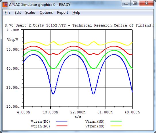
Figure 7: The voltage across a DC-SQUID and the circulating current.

    As an example, Fig,7 shows a simple simulation of the circulating current and the output
voltage of a current-biased dc-SQUID with βC = 0.7, βL = 1.0, with the applied flux of Φ0 /4
and bias current 101% of the SQUID critical current 2IC . (We always use IC to refer to single-JJ
                                                                      2L IC
critical current. We also use slightly nonstandardly the symbol βL = SQ Φ0    for the dimensionless
loop inductance). The APLAC schematic DCSQUID A.N and netlist DCSQUID A.I files are found
in the /anc subfolder, and the result in Fig. 7.
    The circuit contains magnetic mutual coupling between coils L1 and L3, and between L2
and L4. The Prepare statement chooses the Euler method for numeric integration, which works
better with noisy Josephson junctions than the default Trapezoidal method. The bias current is
ramped up to the 20.2µA value during the first 0.1 ns of simulation by using the If-Then-Else
numerical function within the current source definition. Mutual inductance M = 104 pH from
the input coil L3+L4 to the SQUID loop L1+L2 implies response periodicity of 20µA, so that
5µA current ramped up during the first 0.1 ns implies Φ0 /4 applied flux during the simulation.
APLAC components are not completely ideal however, specifically the smallest resistance which
can occur anywhere is 10µΩ as default, if not changed in the Prepare statement. This implies
eg. that the circulating current injected to the SQUID loop during the first 0.1 ns will decay
with time constant of 52 pH/10µΩ = 5µs. Therefore, the longest simulation time should be
significantly shorter than the ‘supercurrent’ decay time.
    In the above plot, the blue trace is the 22 GHz Josephson oscillating voltage, measured from
node N0 and referred to left-hand Y-axis. The green trace is the circulating current in the SQUID
loop, referred to the right-hand Y-axis.

2.1    Filtering to plot SQUID characteristics
When generating SQUID characteristics, it is necessary to filter away the Josephson oscillation
and only retain the average voltage. We implement a 2-pole low-pass filter with a 0.5 GHz
corner frequency to the circuit, utilizing the ideal nature of the components which allows use of

                                                6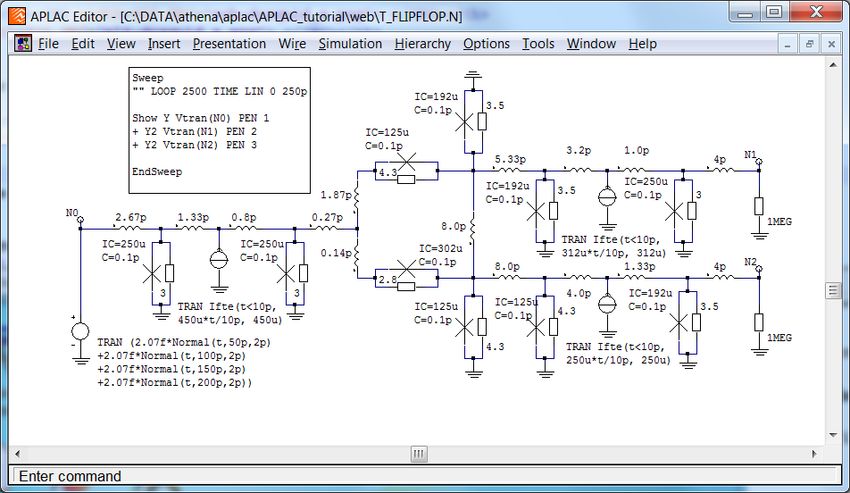
Figure 8: Use of filtering to abtain DC-SQUID characteristics.

               Figure 9: DC-SQUID flux characteristics at several bias current values.

ridiculously low or high values. The corner frequency corresponds to the Josephson frequency at
1µV and should hence work well whenever the voltage across SQUID is larger than a few µV . Due
to settling time of the filter, we must increase the total simulation time. In the example below,
the input coil current is ramped over 60µA i.e. three flux quanta during the 40 ns simulated
time. The APLAC schematic DCSQUID B.N and netlist DCSQUID B.I are found as ancillary files,
results in Fig. 8.
    A set of flux characteristics can be plotted by introducing variables Ix and IbV by the
AplacVar statement and by adding another nested loop to the Sweep. The schematic is DCSQUID C.N
and netlist DCSQUID C.I. The code generates flux-to-voltage characteristics at bias currents
IB = 20.2, 21.2, 22.2 and 23.2 µA, see Fig. 9.
    The responses show the well known IV-curve crossing at half-integer applied flux, due to the
resonance of the loop inductance LSQ and junction capacitances CJ . It is easy to verify that the
crossing disappears if the junction capacitance (hence βC ) is lowered, see Fig, 10.

2.2    Introducing noise
To introduce noise to the circuit, we originally inserted voltage sources representing the Johnson
noise in series with the shunt resistors. Noting that voltage noise density of 8.1 Ω resistors is
43 pV / Hz 1/2 at T = 4.2 K, whose RMS value is 21.7 µV over the 250 GHz Nyquist band1
implied by the 2 ps time step, we included gaussian random number generators with zero mean
  1 Assuming   brickwall frequency response

                                                 7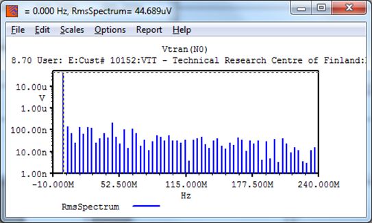
Figure 10: DC-SQUID flux characteristics, LC crossing moved to higher voltage.

                       Figure 11: DC-SQUID with explicit noise sources.

and standard deviation of 21.7 µV . With this approach which we used with the APLAC version
7.61 it was crucial to store the instantaneous noise voltage values into variables at each time
step. This guaranteed that (i) the Nyquist bandwidth is correct, and (ii) the instantaneous noise
voltage didn’t change during the intra-timestep adaptation of the APLAC numerical engine. The
relevant schematic file is DCSQUID D 761.N and netlist file is DCSQUID D 761.I, see Fig.11.
    The more modern version APLAC 8.70 no longer executes the above construct, but rather,
one must trust the APLACs internal noise models. In the example of Fig.12, we have chosen
214 –step (32.768 ns) settling phase followed by a 217 –step (262.144 ns) noise collecting phase.
The initial settling period allows a lower 0.1 GHz corner frequency for the averaging filter. We
first sweep the flux over 1.25 periods in order to get a visual clue of the periodic response for
debugging purposes, and settle at IB = 20.2µA bias, Φ0 /4 applied flux. The added line in the
Prepare statement selects the time discretation step and temperature of the internal APLAC
8.70 noise sources. The resistors in the averaging filter should be defined as noiseless.
    Now, one can rescale the APLAC timetrace to start only after the settling transient, Fig.13
(left). Then from the menus choose Report, Fourier transform with the selections Fast,
RMS, Volts and Rectangular. When the lowest voltage in the Y-scale of the resulting spectral
plot is chosen non-zero (e.g. 1 nV here), it is possible to choose Options, Log Y axis and rescale
the X-axis (frequency) conveniently, resulting the Fig.13 (right).
    The amplitude of the 0 Hz bin, as measured above with the Options, Probe menu selection,
gives correctly the same value as the dc voltage in the time domain trace. From the Fourier
amplitudes the eight bins 3.815, 7.629 . . . 30.517 MHz, sufficently far below the corner frequency

                                                8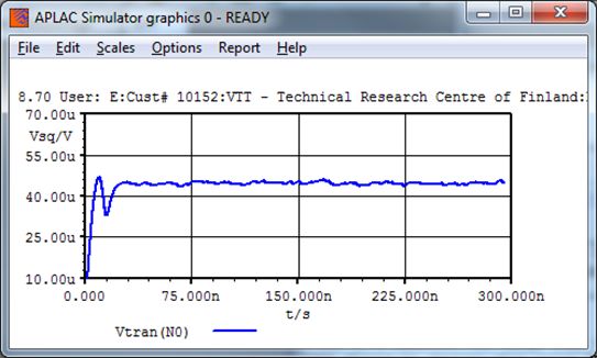
Figure 12: DC-SQUID with internal noise sources.

Figure 13: (Left) Noisy time trace with the initial transient removed by changing the displayed
time start value. (Right) Fourier Transform of the time trace.

of the averaging filter, the root-mean-square sum is 99.3 nVRM S or 51 pV /Hz 1/2 scaled by the
bin width. One could now estimate the steepness dV /dΦ of the flux response of the SQUID at
the setpoint and calculate the effective flux noise. However, we will automate the procedure in
the next example.

2.3    Neat plotting of the spectrum
First, we will automate the Fourier transform, see Fig. 14. To avoid the complications associated
with the averaging filter, we’ll introduce an unfiltered tap named N1. After the settling time has
expired, real part of the time domain signal is stored into a vector variable vrR and imaginary part
equalling zero into vrI. The APLAC’s built-in function Fourier performs the Fourier transform,
where the argument 3 directs the result to be stored stored in magnitude-phase format. In
APLAC,√ the Fourier(3, xxx) returns the amplitude aN of the Fourier term aN sin(nωt + θ),
i.e.    2 times the RMS signal falling within the frequency bin. The second Sweep plots the
generated spectrum, and allows us to format the plot conveniently. X-axis units are FFT bin
numbers. Along the Y-axis there is plotted the RMS voltage noise at the SQUID output, at the
one-bin bandwidth. Schematic and netlist files are DCSQUID E.N, DCSQUID E.I.
     In the next simulation there are two 214 -step initialization intervals followed by one 217
-step noise gathering stage. The first interval lets the simulator settle to the chosen bias and
flux setpoints. In the next interval, SQUID is driven by the sinusoidal flux excitation of 0.1
Φ0 p−p , at frequency which precisely corresponds to the 8th bin of the Fourier transform, for
the sake of determining the SQUID gain dV /dΦ . The plot can be made neater by performing
a 7-point sliding average on the spectral data. Using the knowledge that frequency bins are
∆f = (N ∆t)−1 or 3.815 MHz apart, the X- axis can be scaled into the units of hertz and

                                                 9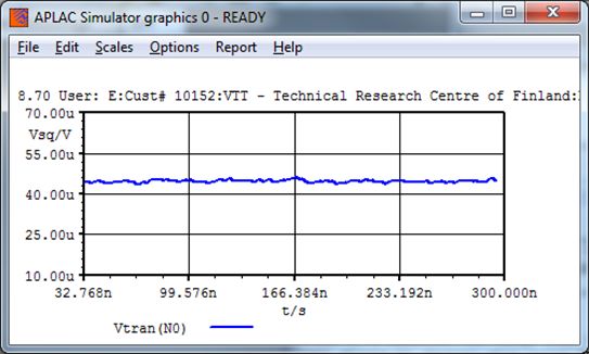
Figure 14: Noisy DC-SQUID with the FFT initiated within code.
Figure 15: Spectral density of the DC-SQUID flux noise.
Y-data into spectral density per Hz 1/2 . Schematic DCSQUID F.N and netlist DCSQUID F.I files.
Finally the measured voltage noise at the SQUID output is scaled by the dV /dΦ into the input-
referred flux noise, Fig.15.
A problem in the previous simulation file is that noise is active also during the dV /dΦ de-
termination stage, which leads to a fluctuating estimate. It is more practical to keep the noise
sources inactive during the gain determination and switch them on for the noise-gathering stage.
This allows use of a lower than 0.1 Φ0 p−p test excitation but neglects the possible noise rounding
of sharp features in the flux characteristics.
In addition to the output voltage, it is possible to obeserve the circulating current in the
SQUID loop, and record its fluctuations to determine the backaction noise. It is also possible
to step through a number of SQUID setpoints automatically, and simulate noise behaviour at
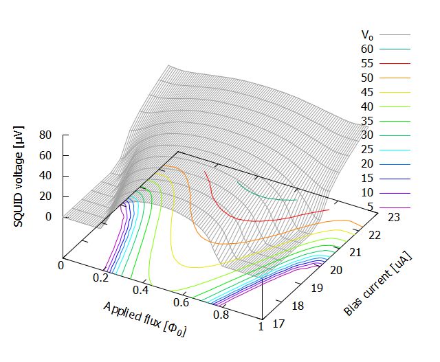
each setpoint. As an example the result of simulating at 100 flux values and at 13 bias current
values is shown in Fig.16. Simulation took 45 minutes on a laptop, when the Show statements
were disabled to avoid the time used for plotting on the computer screen. The calculated data
was stored into files and printed out using GnuPlot.
3 Simulation of Josephson circuits beyond resistively shunted
DC-SQUIDs
Although our primary interest is the noise behaviour of dc SQUIDs and SQUID arrays, other
Josephson junction circuits can be easily simulated, too.
10Figure 16: Voltage, gain dV/dΦ and flux noise of a DC-SQUID as a function of bias current and
applied flux.
Figure 17: RSFQ T flip-flop.
3.1 RSFQ logic
As an example from the domain of RSFQ logic, Fig.17 shows simulation of the T-flipflop, taken
from [7]. APLAC schematic and netlist files are T FLIPFLOP.N and T FLIPFLOP.N. Blue traces are
2ps wide gaussian RSFQ pulses driving the (T)oggle input, referred to the left-hand vertical axis.
Green and red traces are Q and Q outputs of the flipflop, referred to the right-hand vertical axis.
The 10 Josephson junctions are externally shunted to obtain the McCumber-Stewart parameter
of roughly βC = 0.7.
3.2 Beyond the RSJ model
In all the above circuits the Josephson junctions have been resistively shunted with resistors, with
βC ≤1. Although hysteretic JJ circuits can in some cases be simulated without careful modelling
of the quasiparticle behaviour, modelling is straighforward by using controlled sources as non-
linear resistances. In Fig.18 the subgap behaviour of a finite-capacitance Josephson junction is
modelled with an aid of the hyperbolic tangent function. The adjustable parametes are: Vgp
the gap voltage, VgpW width of the subgap-to-normal transition and Rsbg the subgap resistance.
The normal-state resistance Rnn should be set consistent to its Ambegaokar-Baratoff value. The
APLAC JJ W GAP D.N schematic and JJ W GAP D.i netlist are found among the ancilliary files.
Here the bias current of the JJ is swept from IB = 1.6 µA to 156.6 µA in 4 nanoseconds and
back to 1.6 µA in further 4 nanoseconds, motivated by exploring the subgap branch. Finally
there is the 2 ns dwell period at IB = 1.6 µA. In the upper row there is the junction voltage
plotted as a function of the bias current. The voltage-less superconducting branch is followed
11Figure 18: Josephson junction with a model for non-linear subgap resistance (top left). Simulated
current-voltage characteristics of the junction (top right). Time trace of the simulation where
current is ramped up for the first 4 ns and ramped down for the next 4 ns (bottom left). Final 2 ns
of the simulation shows how re-trapping to the zero-voltage state does not occur and Josephson
oscillation persists (bottom right).
12by the jump to the finite-voltage state at the JJ critical current of IC = 100 µA. When the bias
current is lowered, the JJ voltage traverses the finite-voltage quasiparticle branch, and remains
at a finite voltage at the final IB = 1.6 µA. For results see Fig.18.
In the lower row there is shown the junction voltage as a function of simulation time. It
shows more clearly the 200 µV average voltage at the IB = 1.6 µA stationary end state, which
is slightly above the retrap voltage Vrtp for these particular junction model values. Due to this
the junction remains in finite-voltage state indefinitely. If we choose a slightly lower end current
IB = 1.5 µA for the sweep, the JJ decays to the zero-voltage state within the 2 ns dwell time.
There is a magnified plot of the final 2.4 ns of the simulation, where the 100 GHz Josephson
oscillation is more clearly visible.
Above the retrap voltage Vrtp the supercurrent (Josephson) oscillation is so fast that the
shunt capacitance keeps the average voltage across the junction a constant, whereby the quantum
d 2π
phase θ determined by the Josephson relation dt θ= Φ 0
hU i proceeds uniformly. In this case the
supercurrent I(t) = IC sin(θ) averages to zero, so that only the quasiparticle current contributes.
Below Vrtp the instantaneous voltage across the junction varies during the Josephson cycle,
and the supercurrent I(t) = IC sin(θ) does not average to zero. Contribution of the supercurrent
drives the average voltage of the system further downwards, until the system reaches a zero-
voltage state (even at a finite bias current).
4 Simulating Transition Edge Sensors
Superconducting Transition Edge Sensors do not utilize the Josephson effect, but rely on a differ-
ent non-linear phenomenon: the superconductive phase transition [9, 10]. In the APLAC circuit
of Fig.19, we represent the internal temperature as a voltage across the thermal capacitance.
The circuit model [11] was developed in conjunction with the experiment [12]. Plotted is the
TES current (blue) as a function of the bias voltage sweep, which shows the negative dynamic
resistance region characteristic to TESes. The TES current shows the electrothermal oscillation
at a low bias voltages owing to the inductance in series with the bias circuit. The internal
TES temperature is plotted in green. The parameters: R0 is the normal-state resistance, Tc
the transition temperature, DelTwidth of the thermal transition, Ic critical current of the TES
(necessary to get the simulation started) and DelI width of the magnetic/current transition. Rt
is the thermal resistance to the bath and Ct is the heat capacity. The APLAC schematic and
netlist are available as SOFIA TES840.n and SOFIA TES840.i.
The non-linear Voltage Controlled Voltace Source models the TES resistance in terms of the
two control inputs CV(0) and CV(1), representing the TES temperature and current, respectively.
Because mixed-input controlled sources are not possible in APLAC, the linear Current Controlled
Voltage Source is used to transform the TES current into a voltage that can be used for control
purposes. The Voltage Controlled Current Source generates the heat flow driving the thermal
capacitance Ct as the product of TES current and TES voltage.
Additional heat flow (represented as APLAC current) can be arranged to drive the Ct to
simulate absorbed photons. In the circuit of Fig.20 the previous TES model is biased to the
stationary UB = 0.7 µV , and arriving x-ray photons are simulated by 1µs wide heat pulses
whose area is adjusted to correspond the 10 keV photon energy. The Ifte function (if-then-else)
is used to drive the bias voltage from zero to its stationary value. The fmod function (floating-
point modulo) is used to arrange the regular x-ray photon arrival in every 1 ms. The TES current
shows ringing, which implies that the particular TES still close to electrothermal instability at as
low the bias voltage as the UB = 0.7 µV than the shown dc case. In the picture where the voltage
bias is visualized as a negative feedback servo, the electrothermal instability occurs when electric
13Figure 19: A model for Transition Edge Sensors using controlled sources, including magnetically-
induced switching from zero- to finite voltage state.
Joule feedback becomes slower that the thermal time constant of the TES. This can occur if
the series inductance in the bias circuit is too large. The schematic and netlist are available as
SOFIA TES XRAY870.n and SOFIA TES XRAY870.i.
Figure 20: The Transition Edge Sensor model driven with simulated X-ray photon absorption
events.
Of particular interest for us is the case of an AC biased TES, for implementaion of Frequency
Domain Multiplexing. The TES in the Fig.21 is equipped with an LC resonator, and is ac-biased
at 500 kHz, with a slighly higher bias voltage UB = 1 µVRM S . Regardless of higher bias, some
14electrothermal ripple is visible in the zoomed-in time trace, which shows the TES current after
absorption of one x-ray photon. The marginal electrothermal stability is due to LC resonator
settling time to be too slow relative to the thermal time constant, owing to too high Q-factor of
the LC resonator. The APLAC SOFIA TES AC870.n schematic and SOFIA TES AC870.i netlist
are available as ancilliary files.
Figure 21: Ac-biased Transition Edge Sensor modelled with APLAC, taken from [11] (upper).
Magnified time trace of a photon absorption event (lower).
5 Summary
We have found over the years APLAC to be a very useful tool in the design of practical SQUIDs
and in understanding TES dynamics. Its long-standing commercial support and wide range of
library components make it easier to simulate hybrids of Josephson-, TES- and more traditional
electronic circuits. The APLAC facilities for hierarchical design alleviate modelling complex
circuitry.
15References
[1] Martti Valtonen, ”APLAC 2: A flexible dc and time domain circuit analysis program for
small computers”, Technical report, Helsinki University of Technology, Radio Laboratory
(1973).
[2] Martti Valtonen, ”APLAC - A frequency domain program for microwave circuit analysis
and design”, report 1252-79-05, Twente Unversity of Technology (1979).
[3] S. R. Whiteley, “Josephson junctions in SPICE3,” IEEE Tran. Magn., vol. 27, no. 2, pp.
2902-2905, doi:10.1109/20.133816 (1991).
[4] E. S. Fang and T. van Duzer, “An Efficient Method for Finding dc Solutions for Josephson
Circuits,” IEEE Tran. Appl. Supercond., vol. 1, pp. 126-133, doi:10.1109/77.84626 (1991).
[5] Tapani Ryhänen and Heikki Seppä, ”Effect of parasitic capacitance and inductance on the
dynamics and noise of dc superconducting quantum interference devices”, J. Appl. Phys.,
vol. 71, 6150, doi:10.1063/1.350424 (1992).
[6] Mikko Kiviranta and Heikki Seppä, ”Noise behaviour of the un SQUID studied by numerical
simulation”, IEEE Tran. Appl. Supercond. vol. 7, pp. 3224-7, doi:10.1109/77.622033 (1997).
[7] S. V. Polonsky et al., ”New RSFQ circuits (Josephson junction digital devices)”, IEEE Tran.
Appl. Supercond., vol. 3, pp. 2566-77, doi:10.1109/77.233530 (1993).
[8] C. D. Tesche and J. Clarke, ”Dc SQUID: noise and optimization”, J. Low Temp. Phys., vol.
29, pp. 301-31 doi:10.1007/BF00655097 (1977).
[9] K. Irwin and G. Hilton, ”Transition-edge sensors”, Cryogenic Particle Detection,
doi:10.1007/10933596 3 (2005).
[10] The article on TESes in Wikipedia.
[11] M. Kiviranta et al., SQUID Multiplexers for Transition Edge Sensors, presented in the
NASA 2002 Far-IR, Sub-mm & mm Detector Technology Workshop.
[12] J. van der Kuur et al., ”Performance of an ac biased TES microcalorimeter”, Appl. phys.
Lett., vol. 81, 4467, doi:10.1063/1.1526168, (2002).
16You can also read