"PV research in Neuchâtel: from high efficiency crystalline cells to novel module concepts" - Laure-Emmanuelle Perret-Aebi, Christophe Ballif ...
←
→
Page content transcription
If your browser does not render page correctly, please read the page content below
„PV research in Neuchâtel: from high
 efficiency crystalline cells to novel
          module concepts”

         Laure-Emmanuelle Perret-Aebi, Christophe Ballif
         April 11th 2014
         Congrès Photovoltaïque National 2014, Lausanne
Competence center for research in Photovoltaics
                                 CSEM PV-center founded in 2013
                                  First swiss technology transfer
                                  for photovoltaics with CH base
                                  funding

                                      • Coating technologies
                                      • High efficiency c-Si
                                      • Modules and systems

  • Basic researches
  • Advanced devices
  • SHJ cells
      EPFL- PVLAB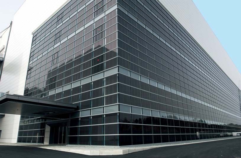
PV research activities in Neuchâtel, Switzerland
Silicon heterojunction Thin-film silicon Module
(SHJ) cells cells Technology &
systems
High efficiency Aesthetic and
Ultra-low cost
Low cost reliable, grid
• Plasma processes for
Advanced use of
semiconductor active and doped layers
coating
technologies • CVD (chemical vapor deposition) and sputtering
doped transparent conductive layers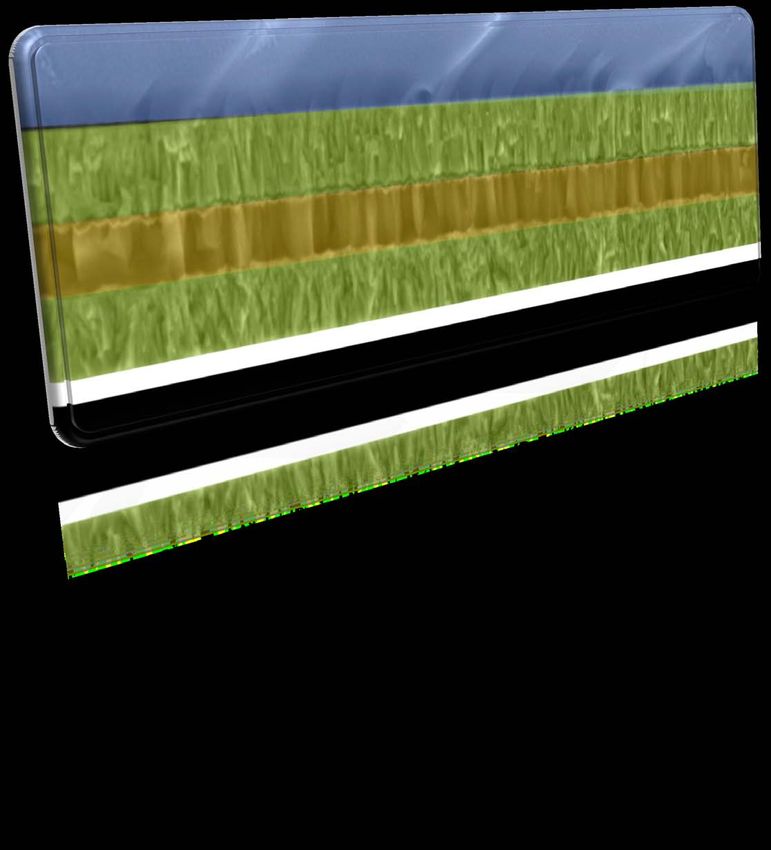
St-Exupéry, The Little Prince…

                        Please draw me the
                     perfect solar cell and the
                      most beautiful module…

     3
A quasi-perfect solar cell
                                     And the winner is:

• Would capture most of the
  light below the bandgap
• Would have “membranes”
                               • Random pyramids is an
  on both sides which collects
                                 excellent optical system,
  selectively all
                               • Passivated contacts for
  photogenerated electrons       electrons and holes
  and holes                    • Silicon is low cost
• Would be be low cost

      4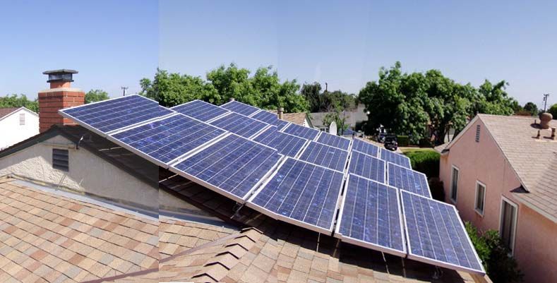
High efficiency crystalline Si cells

       Silicon heterojunction cells:
       An excellent candidate for quasi-ideal devices
       With few production steps

                    5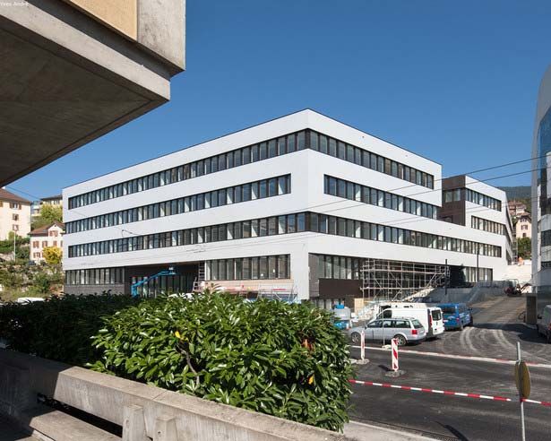
From homo- to heterojunction solar cell
Diffused junction solar cell
Direct contact between
absorber and metal
=
Recombinative contact
Lower Voc
Heterojunction solar cell
Thin semiconductor layer between
absorber and metal
=
Passivated contact
Higher Voc
6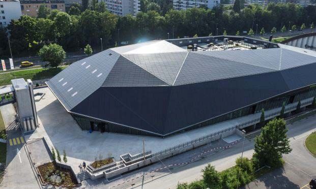
Processing sequence                                        all processing < 200 degr. C

Chemical           PECVD I      PECVD II       PVD        Metallization
  baths            Intrinsic     Doped film                 Screen
                                               TCO          printing
c-Si surface       film          deposition
                                               sputtering   and curing
preparation        deposition    a-Si:H(n/p)
                   a-Si:H(i)                                at 200°C

               7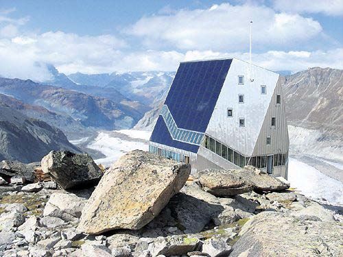
Becoming a mainstream technology ?
                                          Increase R&D
                                          activities.

                                          Several groups
                                          and industries
                                          above 20% with
                                          screen-printing or
                                          plated contacts
                                          (CIC, INES/EDF,
                                          ISFH, Kaneka,
                                          R&R, LG,
                                          Hyunday,…….)

                                          + activities at ISE,
                                          HZB

                                      Efficiency        Voc

                                       24.7%          750 mV
                                                   Panasonic, Japan

[De Wolf et al, Green 2, 7 (2012).]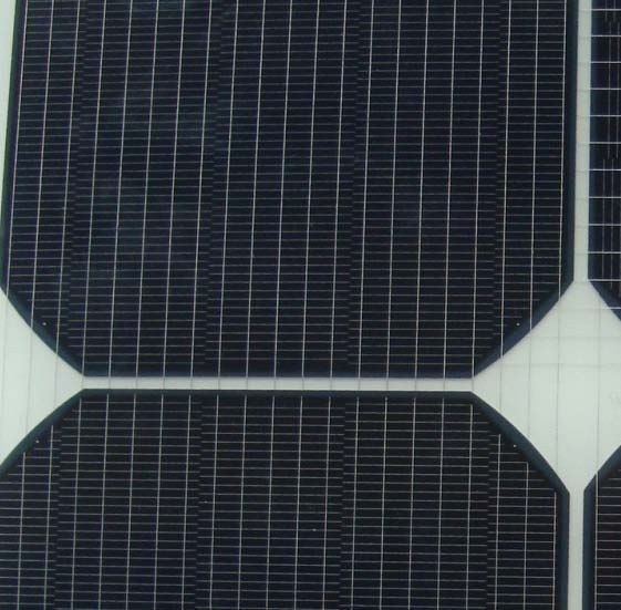
Best screen-printed cells after optimization (4 cm2)
• Independently confirmed results
(Fraunhofer ISE CalLab)
n-type p-type
area [cm2] 3.98 3.98
Voc [mV] 727 722
Jsc [mA/cm2] 38.9 38.4
FF [%] 78.4 77.1
Efficiency [%] 22.14 21.38
(screen-printed contacts)
Record efficiency for full SHJ p-type solar cells
Best Voc : 726 mV record Voc for any p-type c-Si solar cellHigh efficiency SHJ solar cell
• Cell area : 4 cm2
• PECVD layers in Octopus II
• IO:H-ITO front bilayer TCO + AR
• To be compared with baseline 22% screen-
printed cells
Eff. 22.4%
N.b. Sees also results of P. Papet al.
22.3% on 5” cells, results of INES, results of
Kaneka with 24.2%Rear-contacted IBC-SHJ
Fully back contacted solar cells
• Simple process with hard mask for p and n
• And hotmelt print to separate TCO,
• 9 cm2 solar cell.
45
40
Current density (mA/cm2)
35
30
25
VOC = 724 mV
20
JSC = 39.9 mA/cm2
15
10 FF = 74.5%
5 Eff. = 21.5%
0
0 100 200 300 400 500 600 700 800
Voltage (mV)
[A. Tomasi, B. Paviet-Salomon, et al, submitted (2014).]Cost of metallization move away from standard design
Cu Plating
[Kakeka]
J. L. Hernandez, et al. T..
D. 21st PVSEC, Fukuoka,
5 busbars 2011, 3A-1O-05.
[R&R CH]
P. Papet et al.
D. Bätzner et al.
Proc. 26th EU-PVSEC
2011
Cu paste
Arrays of wire [AIST, JP]
Yoshida et al. Proc. 26th
[Day4 –MBT] EU-PVSEC 2011
Balllif et al.Alternative approaches for metallization : “smart wires”
6” Cz
• Low Ag content (< 40 mg/cell)
• Aesthetic
From Roth & Rau Research, by courtesy of Dr. B. Strahmsponsored by
SWISS INNO HJT
PROJECT
FULLY INTEGRATED 3 years PROJECT:
PILOT AND DEMONSTRATION OF HJT TECHNOLOGY
- Diamond wire wafering
- Pilot Cell Production Line in Hauterive – NE
- Advanced Metallization Pilot Line
- SmartWire Module Interconnection
- Dedicated cell and module metrology
- Outdoor monitoring of 3 generations of modules
developed in the projectSome recent results on thin film silicon at IMT PV-Lab
Thin-film silicon solar cells Light scattering at
nanotextured interface
Glass Substrate
Front Electrode
(transparent)
Silicon Layers
Silicon Layers: 1 or 2 p-i-n junctions out Back Electrode
of amorphous and microcrystalline Si Back ReflectorStatus of µc-Si:H single junction cells
P. Cuony et al., APL, 2011
• 1.8-µm-thick i-layer, Rc = 57%
• SiOx in cell design G. Bugnon et al.,
SolMat, 2013
• Single layer LPCVD ZnO electrodes
• In- house AR texture on the glass
M. Despeisse et al.,
• White paste back reflector PSS-A, 2011
10.7%
(certified)
S. Hänni et al., PIP 2013High-efficiency micromorph cell
• Single 2.3 µm LPCVD front electrode
• 230-nm-thick top cell
• 60-nm-thick SiO-IRL
• 2.2 µm bottom cell
• Full SiO design for the bottom cell
initial 1000 h
LS
Voc (V) 1.38 1.36
FF (%) 76.1 71.4
Jsc (mA/cm2) 12.8 12.7
Eff (%) 13.4 12.3High-efficiency triple junction cell (initial)
2 1.0
top (10.01)
0 mid (9.77)
VOC = 1.89 V 0.8 bot (9.76)
tot (29.54)
JSC (mA/cm2)
-2 FF = 74.4%
JSC = 9.76 mA/cm2
0.6
EQE
-4 Eff = 13.7%
-6 0.4
-8
0.2
-10
0.0
-1.0 -0.5 0.0 0.5 1.0 1.5 2.0
400 500 600 700 800 900 1000 1100
V (V) λ (nm)
Also obtained: Jsc tot > 30 mA/cm2 on rougher front electrode
Jsc ~ 31 mA/cm2 on replicated front structure + IO:H
Voc = 1.91 V on flatter front electrodeHigh-efficiency triple junction cell (stabilized)
2 1.0
Top (9.66)
0 Mid (9.58)
0.8 Bot (9.64)
Tot (28.88)
J (mA/cm2)
-2
VOC = 1.85 V
0.6
EQE
FF = 72.5%
-4 JSC= 9.58 mA/cm2
Eff = 12.8% 0.4
-6
-8 0.2
-10 0.0
-0.5 0.0 0.5 1.0 1.5 2.0 400 500 600 700 800 900 1000 1100
V (V) λ (nm)
12.8% Stable for p-i-n aμμ triple (6% rel degradation)Thin-film devices
Abundant & non-toxic materials
Low cost / m2
Building integration
Hot-climate environment
Consumer electronicsMaterial, Process and Reliability
• Development of new encapsulation materials
Reliability Failure mode
identification,
– accelerating aging tests,
modelisation
– mechanical tests,
New module
– adhesion, design
– optical properties, Demonstrate >30
years lifetime module
– chemical characterization
• Lamination process
optimization,
Electricity cost
–temperature and pressure, reduction
–rheology
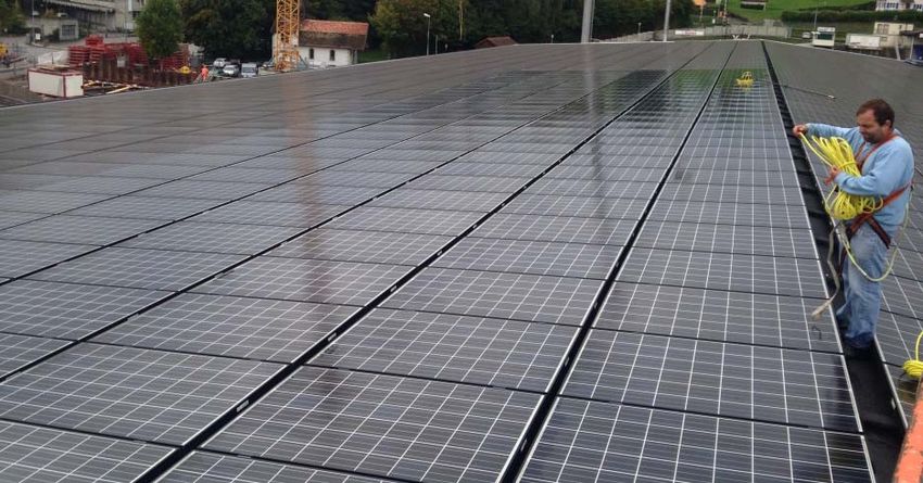
–interconnectionBuilding Integrated Photovoltaics (BIPV) Let’s try to avoid ugly solar….
Building Integrated Photovoltaics (BIPV)

  Let’s try to avoid ugly solar….
Building Integrated Photovoltaics (BIPV)
Building Integrated Photovoltaics (BIPV)

• Development of attractive BIPV products:
     • Attractive dedicated modules for architects
           colored modules,
           optical effect,
           size, shape, dummies

     • Multi-functional building elements
           building skin,
           insulation,
           windows.

                                                     Archinsolar project
Mission: enabling massive PV deployment
• PV system performance
• Evaluation of components and topologies
• Operation and maintenance strategies
• Distributed energy storage:
• Characterisation of components
• Control strategies
• Residential micro-grids
• Product development for application-specific PV
systemsPotential of PV in Switzerland
Well oriented roofs in Switzerland
• 30% of yearly electricity needs with 12% modules =130 km2 roofs or
less than 3 % of built surface
Minimum impact on the landscapeThank you for your attention
You can also read