SURFACE MORPHOLOGY AND X-RAY PHOTOELECTRON SPECTROSCOPY OF BIFEO3 THIN FILMS DEPOSITED ON TOP OF TA2O5/SI LAYERS
←
→
Page content transcription
If your browser does not render page correctly, please read the page content below
E3S Web of Conferences 295, 04009 (2021)                                 https://doi.org/10.1051/e3sconf/202129504009
WFSDI 2021

       Surface morphology and X-ray photoelectron
       spectroscopy of BiFeO3 thin films deposited on
       top of Ta2O5/Si layers
       Shikhgasan Ramazanov1, Ştefan Ţălu2,*, Rashid Dallaev3, Guseyn Ramazanov4, Pavel
       Škarvada3, Jindřich Oulehla5, Dinara Sobola3,6, and Dmitry Nazarov7
       1Dagestan   State University, Makhachkala, St. M. Gadjieva 43-a, Dagestan Republic, 367000, Russia
       2The   Technical University of Cluj-Napoca, The Directorate of Research, Development and
       Innovation Management (DMCDI), Constantin Daicoviciu Street, no. 15, Cluj-Napoca, 400020, Cluj
       county, Romania.
       3Brno University of Technology, Faculty of Electrical Engineering and Communication, Physics

       Department, Technická 8, 616 00 Brno, Czech Republic.
       4Dagestan State Technical University, Makhachkala, St. I. Shamil, 70, Dagestan Republic, 367026,

       Russia
       5Institute of Scientific Instruments of the Czech Academy of Sciences, Královopolská 147, 612 64

       Brno, Czech Republic
       6Institute of Physics of Materials, Academy of Sciences ČR, Žižkova 22, 616 62, Brno, Czech

       Republic
       7Ural State University of Economics, Institute of management and information technologies, Russian

       Federation

                     Abstract. In this study a comparison of the topography of BiFeO3 (BFO)
                     thin films deposited on tantalum pentoxide substrates of different
                     thicknesses is provided. The Ta2O5 substrates had a roughness increasing
                     with the film thickness. The relationship between substrates of different
                     topography but the same composition with the quality of the growing
                     bismuth ferrite film is estimated. For the first time the topography
                     estimation of BFO on Ta2O5 is presented. The difference in temperature
                     expansion coefficients leads to intensive evaporation of bismuth ferrite
                     from the surface during annealing. XPS analysis is provided for as-
                     deposited and annealed BFO layers.

       1 Introduction
           Data storage and processing centers are large consumers of energy resources due to the
       development of cloud storage services, social networks, mobile applications. The use of
       new electronic components is a necessary condition for the further growth of capacities and
       rates of functioning of these resources. Such elements include logical elements of a new
       type, memristors, which are the basis of non-volatile memory with a high density of

       *
           Corresponding author: stefan_ta@yahoo.com

© The Authors, published by EDP Sciences. This is an open access article distributed under the terms of the Creative Commons
Attribution License 4.0 (http://creativecommons.org/licenses/by/4.0/).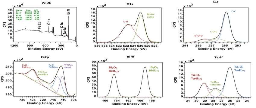
E3S Web of Conferences 295, 04009 (2021)                      https://doi.org/10.1051/e3sconf/202129504009
WFSDI 2021

      information storage, etc. Owing to its attractive optical and electrical properties tantalum
      pentoxide (Ta2O5) attracts ever increasing attention of the scientific community nowadays
      [1]. High dielectric constant and large RI (refractive index) make Ta 2O5 an excellent
      candidate to be considered in a number of various applications. For instance, it can serve as
      an insulating material in all sorts of “sandwich” structures such as MIS
      (metal/insulator/semiconductor) or MIM (metal/insulator/metal) [2,3]. Another possible
      application of Ta2O5 emerges due to its ability to withstand harsh environments, high
      temperatures and overall chemical sturdiness/inertness. Therefore, thin films of Ta 2O5 may
      also be utilized as protective players in various sensors, detectors and other electronics
      which might benefit from extra shielding against aggressive media and corrosion. Low
      absorption coefficient along with large refractive index is absolutely essential when it
      comes to antireflective coatings which is why Ta2O5 find its use in solar cells fabrication as
      well. Such optical properties are also sought after during manufacture of optical filters and
      photonic crystals. Biological industry may also benefit from the inclusion of Ta 2O5 since it
      has been shown to be a viable choice for production of biochemical and biological sensors
      and detectors [4,5]. Protein detection and hydrogen ion sensing membranes are some of the
      examples of theses sensors/detectors. Aforementioned were only the explored applications
      of the Ta2O5 but one may already conclude that it is a quite promising material, however,
      preparation of Ta2O5 is a rather challenging procedure. There is great amount of methods
      which allow obtaining Ta2O5 with various degrees of success. Among those methods are
      methods of chemical vapour deposition (CVD) group: spray pyrolysis, atomic layer
      deposition, sol-gel methods; and physical vapour deposition (PVD) group: magnetron
      sputtering, ion assisted coating technique, thermal evaporation coating etc. [6–8]. However
      due to Ta2O5 specific chemical nature a usage sol-gel ablation method is recommended. BFO
      has a small band gape of ~2.8 eV. It is a chemically stable compound. According to the latest
      literature reports, BFO thin films are utilized as photocatalysts, due to their remarkable
      photocatalytic activity in the visible light spectrum [9,10]. Other applications of BFO include
      gas sensors and solar cells [11]. The Ta2O5 is also an optical material, and with thin films
      BFO will allow the use of these compositions in optical magnetic applications. The ALD
      method makes it possible to obtain 100% conformal films on the surface of substrates, which
      is relevant to the application of this method in the mentioned applications.

      2 Experimental results
          The films of BFO composition were prepared by atomic layer deposition (ALD) at
      ALDCERAM ML-200 device. Samples were obtained by layer-by-layer growth of BiOx
      and FeOx. The source for bismuth component was Bi(mmp) 3 and ferrocene was the source
      of iron Fe(C5H5)2. The experiment was repeated in accordance with the preparation of thin
      BFO films in our previous experiments on the substrate surface of highly oriented pyrolytic
      graphite [12,13] and TiO2 nanotubes [9,10]. In this work, Ta2O5/Si heterostructures were
      used as substrates [14] with thickness of Ta2O5 from 20 up to 100 nm. After obtaining the
      films, heat treatment was carried out in vacuum at temperature of 600 oC during 1 hour.

      2.1 Atomic force microscopy data
          AFM images of Ta2O5 with different thickness are given in Figure 1. The general
      tendency here is that the average surface roughness of the Ta2O5 layer grows with
      thickness. Right choice of scanning parameters [15-17] are important to obtain reliable
      results [18–22] with high resolution [23–26] to characterise the 3D surface microtexture
      and micromorphology [27-30].
          Table 1 shows the characteristics of the AFM scanning in details.

                                                    2
E3S Web of Conferences 295, 04009 (2021)                             https://doi.org/10.1051/e3sconf/202129504009
WFSDI 2021

                                    Table 1. Parameters of AFM images acquisition.
           Scanning probe microscope                   Dimension Icon with Scan Asyst
           Mode                                        ScanAsyst
           Scan sizes                                  500 nm and 1 um
           Aspect ratio                                1
           Scan rate                                   0.639 Hz
           Samples/line                                608
           FeedBack Gain                               from 17 to 19
           Peak Forse Set Point                        477 pN
           Peak Force Amplitude                        150 nm
           Peak Force Freq                             2 kHz
           Lift Height                                 25.1 nm
           Sprint constant of Cantilever               0.4 N/m
           Probe model                                 Scanasyst-air
           Material                                    Silicon Tip on Nitride Lever
           Tip Radius (Nom)                            2 nm

           Figure 1 shows the surface topography of the Ta2O5 layers depending on the thickness.

                                                                b)
      a)

      c)
                                                                d)

                                                           e)

           Fig. 1. Topography of Ta2O5 films with thickness of: a) 20 nm; b) 40 nm; c) 60 nm; d) 80 nm; e)
                                                    100 nm.

                                                       3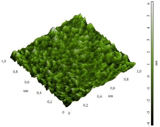
E3S Web of Conferences 295, 04009 (2021) https://doi.org/10.1051/e3sconf/202129504009
WFSDI 2021
As shown in Figure 1, the topography of the film surface varies insignificantly
depending on the thickness (from 20 nm to 100 nm): the difference of heights with a
change of thickness (every 20 nm) is about 0.1 - 0.2 nm. A distinctive feature of hetero-
epitaxial growth [31,32] is the formation of a pseudocubic structure of the resulting film
due to the lattice mismatch between the substrate and the film. Such crystallization is
typical for ion-plasma methods, where additional kinetic energy of the sprayed particles is
involved. In the case of the ALD method, a chemical reaction occurs on the surface and
only during heat treatment crystallites are formed on the surface. It was noted that thin
Ta2O5 films were formed by the fractal mechanism [33]. This work also studied the
correlation between the thickness of Ta2O5 thin films and their 3D micromorphology.
Probably, thin BFO films repeat this growth mechanism at small thicknesses (~ 50 nm).
a) b)
c) d)
e)
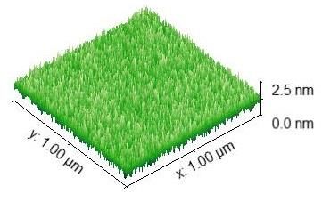
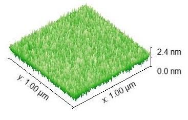
Fig. 2. Topography of the BFO film obtained on the surface of Ta2O5 layers with a thickness of:
a) 20 nm; b) 40 nm; c) 60 nm; d) 80 nm; e) 100 nm
4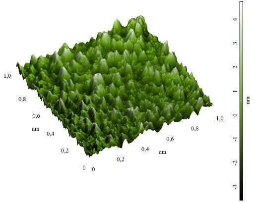
E3S Web of Conferences 295, 04009 (2021) https://doi.org/10.1051/e3sconf/202129504009
WFSDI 2021
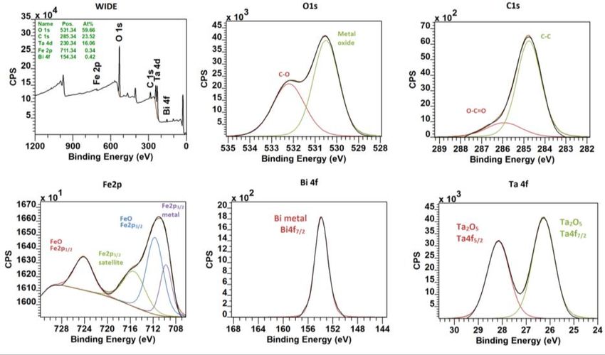
2.2 X-ray photoelectron spectroscopy data
The study of chemical conditions of the surface (5-10nm) was made by XPS (AXIS
SupraTM). The XPS spectra of as-deposited BFO layers are given in Figure 3. Figure 4
contains spectra for the same layers after annealing procedure.
Fig. 3. XPS spectra of the deposited BFO films before annealing
Fig. 4. XPS spectra of the deposited BFO films after annealing
By taking a look at the wide spectra of both as-deposited and annealed layers it can be
inferred that the elemental ratio on the surface changes drastically after the annealing. The
most noticeable change is the sharp decrease of the overall oxygen concentration. Another
aspect worth mentioning is the increase of intensity of other elements such as Bi, Ta and
Fe. The most plausible explanation to this is that the deposited samples had a few nm oxide
layers on the surface. This oxide layer caused the overshadowing effect, due to which the
high concentration of oxygen made other peaks appear low on the spectrum. Annealing,
5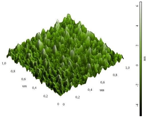
E3S Web of Conferences 295, 04009 (2021)                      https://doi.org/10.1051/e3sconf/202129504009
WFSDI 2021

      apparently, removed the bulk of the surface oxide layer and the concentration profile has
      become more resembling of the actual concentration expected within the BFO layers. High
      resolution spectra provided in both figures also exhibit quite a bit of change. One can
      observe the change in the concentration of the certain bonds in the O1s and Fe2p spectra.
      C1s, Ta4f and Bi4f spectra on the other hand demonstrate formation/revelation of the
      entirely new bonds.

      3 Conclusion
          In this study BFO thin films were deposited on the surface of Ta2O5 with different
      thickness values. According to AFM, BFO films deposited on Ta2O5 layer with higher
      thickness also have higher values of the average surface roughness. Additionally, XPS
      analysis of the surface of BFO layers has been conducted. Spectra were demonstrated for
      as-deposited and annealed layers. According to the acquired data, as-deposited layer had a
      few nm oxide layers which was removed by to a large extent the annealing procedure.

          Research described in this paper was financially supported by Internal Grant Agency of Brno
      University of Technology, grant No. FEKT-S-20-6352. CzechNanoLab project LM2018110 funded
      by MEYS CR is gratefully acknowledged for the financial support of the measurements/sample
      fabrication at CEITEC Nano Research Infrastructure.

      References
      1  X. Li, Y. Wang, F. Wang, A. Liang, Mater. Lett. 298, 130000 (2021).
         https://doi.org/10.1016/j.matlet.2021.130000.
      2 R. Wang, L. Pan, Q. Han, H. Zhu, M. Wan, Y. Mai, J. Alloys Compd. 865, 158931
         (2021). https://doi.org/10.1016/j.jallcom.2021.158931.
      3 S. Das, V.K. Singh, Photonics Nanostructures - Fundam. Appl. 44, 100904 (2021).
         https://doi.org/10.1016/j.photonics.2021.100904.
      4 Y. Nishimura, A. Shinkawa, H. Ujita, M. Tsuji, M. Nakamura, Appl. Surf. Sci. 136,
         22–28 (1998). https://doi.org/10.1016/S0169-4332(98)00332-8.
      5 A.K. Narasimhan, S.L. Balasubramanian, G. Krishnamurthi, Mater. Lett. 300, 130214
         (2021). https://doi.org/10.1016/j.matlet.2021.130214.
      6 Y. Ito, Y. Abe, M. Kawamura, K.H. Kim, T. Kiba, Thin Solid Films. 710, 138276
         (2020). https://doi.org/10.1016/j.tsf.2020.138276.
      7 J. Zheng, K. Wen, Y. Liu, L. Gao, Z. Ma, X. Diao, Ceram. Int. 46, 3875–3881 (2020).
         https://doi.org/10.1016/j.ceramint.2019.10.113.
      8 L. Parshina, O. Novodvorsky, O. Khramova, D. Gusev, A. Polyakov, V. Mikhalevsky,
         E.      Cherebilo,      Chaos,       Solitons    and      Fractals.    142 (2021).
         https://doi.org/10.1016/j.chaos.2020.110460.
      9 F.F. Orudzhev, S.M. Ramazanov, A.B. Isaev, N.M. Alikhanov, D. Sobola, M.Y.
         Presniakov,          Mater.        Today        Proc.         2018–2021    (2020).
         https://doi.org/10.1016/j.matpr.2020.04.153.
      10 F. Orudzhev, S. Ramazanov, D. Sobola, A. Isaev, C. Wang, A. Magomedova, M.
         Kadiev,        K.      Kaviyarasu,       Nanomaterials.      10,      1–16 (2020).
         https://doi.org/10.3390/nano10112183.
      11 B.G.          Park,        Mater.         Lett.      285,         129006   (2021).
         https://doi.org/10.1016/j.matlet.2020.129006.

                                                    6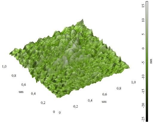
E3S Web of Conferences 295, 04009 (2021)                   https://doi.org/10.1051/e3sconf/202129504009
WFSDI 2021

      12 S. Ramazanov, D. Sobola, F. Orudzhev, A. Knápek, J. Polčák, M. Potoček, P. Kaspar,
         R. Dallaev, Nanomaterials. 10, 1–18 (2020). https://doi.org/10.3390/nano10101990.
      13 D. Sobola, S. Ramazanov, M. Koneĉnỳ, F. Orudzhev, P. Kaspar, N. Papež, A. Knápek,
         M. Potoĉek, Materials (Basel). 13 (2020). https://doi.org/10.3390/ma13102402.
      14 P. Kaspar, P. Škarvada, V. Holcman, L. Grmela, Appl. Phys. A Mater. Sci. Process.
         125 (2019). https://doi.org/10.1007/s00339-019-3134-3.
      15 A. Knápek, D. Sobola, D. Burda, A. Daňhel, M. Mousa, V. Kolařík, Nanomaterials. 9
         (2019). https://doi.org/10.3390/nano9121756.
      16 Ş. Ţălu, R.P. Yadav, O. Šik, D. Sobola, R. Dallaev, S. Solaymani, O. Man, Mater. Sci.
         Semicond. Process. 85, 15–23 (2018). https://doi.org/10.1016/j.mssp.2018.05.030.
      17 N. Papež, A. Gajdoš, R. Dallaev, D. Sobola, P. Sedlák, R. Motúz, A. Nebojsa, L.
         Grmela, Appl. Surf. Sci. 510 (2020). https://doi.org/10.1016/j.apsusc.2020.145329.
      18 A. Méndez, Y. Reyes, G. Trejo, K. Stępień, Ş. Ţălu, Microsc. Res. Tech., 78, 1082
         (2015)
      19 Ş. Ţălu, S. Stach, D. Raoufi, F. Hosseinpanahi, Electron. Mater. Lett., 11, 749 (2015)
      20 A.R. Grayeli-Korpi, C. Luna, A. Arman, Ş. Ţălu, Results Phys, 7, 3349 (2017)
      21 Ş. Ţălu, S. Stach, A. Mahajan, D. Pathak, T. Wagner, A. Kumar, R.K. Bedi, M. Ţălu,
         Electron Mater Lett., 10, 719 (2014)
      22 Ş. Ţălu, Z. Marković, S. Stach, B.T. Marković, M. Ţălu, Appl. Surf. Sci., 289, 97
         (2014)
      23 D. Sobola, Ş. Ţălu, S. Solaymani, L. Grmela, Microsc. Res. Tech., 80, 1328 (2017)
      24 Ş, Ţălu, I.A. Morozov, R.P. Yadav, Appl Surf Sci., 484, 892 (2019)
      25 Ş. Ţălu, A.J. Ghazai, S. Stach, H.A. Hassan, Z. Hassan, M. Ţălu, J. Mater. Sci. Mater.
         Electron., 25, 466 (2014)
      26 Ş. Ţălu, Micro and nanoscale characterization of three dimensional surfaces. Basics
         and applications. (Napoca Star Publishing House, Cluj-Napoca, Romania, 2015).
      27 Ş. Ţălu, M. Bramowicz, S. Kulesza, V. Dalouji, S. Solaymani, S. Valedbagi, Microsc.
         Res. Tech., 79, 1208 (2016)
      28 A. Jafari, M.H. Alam, D. Dastan, S. Ziakhodadadian, Z. Shi, H. Garmestani, A.S.
         Weidenbach, Ş. Ţălu, J Mater Sci: Mater Electron, 30, 21185 (2019)
      29 A. Jafari, K. Tahani, D. Dastan, S. Asgary, Z. Shi, X.T. Yin, W.D. Zhou, H.
         Garmestani, Ş. Ţălu, Surf Interfaces, 18, article 100463 (2020)
      30 Ş. Ţălu, S. Stach, J. Zaharieva, M. Milanova, D. Todorovsky, S. Giovanzana, Int J
         Polym Anal Ch., 19, 404 (2014)
      31 Ş. Ţălu, S. Sebastian, R. Shikhgasan, S. Dinara, R. Guseyn, Mater. Sci. Pol. 35, 539–
         547 (2017). https://doi.org/10.1515/msp-2017-0049.
      32 S.M. Ramazanov, G.M. Ramazanov, Tech. Phys. Lett. 40, 44–47 (2014).
         https://doi.org/10.1134/S106378501401009X.
      33 D. Sobola, P. Kaspar, J. Oulehla, Ş. Ţălu, N. Papež, Mater. Sci. Pol. (2020).
         https://doi.org/10.2478/msp-2019-0083.

                                                 7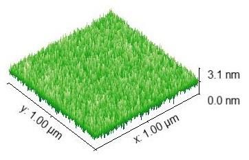
You can also read