The LANL C-Band Engineering Research Facility (CERF-NM) Test Stand Installation, Operation and Initial Conditioning.
←
→
Page content transcription
If your browser does not render page correctly, please read the page content below
The LANL C-Band Engineering Research Facility
(CERF-NM) Test Stand Installation, Operation and
Initial Conditioning.
Mark E. Middendorf, LANSCE AOT-RFE, on behalf of:

J.T. Bradley III, C.E. Buechler, R.L. Fleming, E.G. Geros, D.V. Gorelov, H.J. Guas III,
M.K. Kirshner, F.L. Krawczyk, J.W. Lewellen, L.N. Merrill, R.C. Moore, M.E. Schneider,
E.I. Simakov, T. Tajima.
April 21, 2021

LA-UR-21-22377 V2

 Managed by Triad National Security, LLC., for the U.S. Department of Energy’s NNSA. 04/21/2021 1
Acronyms and Abbreviations

LANSCE: Los Alamos Neutron Science Center
AE: Accelerator Engineering
AOT: Accelerator Operations and Technology
CCPS: Capacitor Charging Power Supply
FPS: Filament Power Supply
IPC: Ion Pump Controller
MCU: Main Control Unit
MDE: Mechanical Design Engineering
OSH - DS: Occupational Safety and Health – Deployed Services
PDU: Power Distribution Unit
RFE: Radio Frequency Engineering
RP - FS: Radiation Protection – Field Service
SU: Switch Unit
SPS: Solenoid Power Supply

 4/21/2021 2
Agenda

1. Introduction
2. Acknowledgements
3. Timeline
4. Klystron Modulator
5. Waveguide and Waveguide Components
6. LLRF, Data Acquisition and Control
7. Initial Conditioning Efforts
8. Conclusion

 4/21/2021 3
Introduction
• The C-Band Engineering Research Facility
 (CERF-NM) is the first such installation in
 the US to provide ultra-high peak power
 (up to ~50MW) radio-frequency (RF) test
 capability in the C-band (5.712 GHz)
 frequency range.

• Funded by a 2020 Laboratory Directed
 Research and Development (LDRD)
 award, the facility will be used for
 evaluating novel high-gradient
 accelerating structures.

• Internal collaborators; Accelerator Operations and Technology (AOT), Engineering
 Technology and Design (E), and Sigma Divisions.
• External collaborators; University of California, Los Angeles, SLAC National
 Accelerator Laboratory, and Stanford University.

• This talk focuses on the klystron/modulator installation and integration, and the initial
 conditioning and commissioning efforts.

 04/21/2021 4
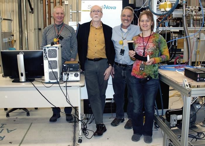
Acknowledgements

Frank Krawcyk, LANL LANSCE AOT-AE, (Retired)
Mark Kirshner, LANL LANSCE AOT-RFE, (Retired)
Evgenya (Jenya) Simakov, LANL LANSCE AOT-AE
Sylvie Adam, LANL LANSCE, OSH-DS
Kevin Andrews, LANL LANSCE RP-FS
Jon Bergemann, LANL LANSCE AOT-RFE
Cindy Buechler, LANL LANSCE AOT-MDE
Ryan Fleming, LANL LANSCE AOT-AE
Ernie Geros, LANL LANSCE AOT-RFE
Paul Martin, LANL LANSCE OSH-DS
Rosliann Miller, LANL LANSCE RP-RS
Robert Moore, LANL LANSCE AOT-MDE
Manuelita Rodriquez, LANL LANSCE AOT-RFE
Keith Stephens, LANL LANSCE AOT-MDE

 4/21/2021 5
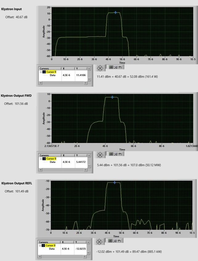
Timeline

• August 30, 2019; Klystron/Modulator Factory Acceptance Test.

• September 23 to September 27, 2019; Installation at LANL.

• January 30 to February 21, 2020; Conditioning at LANL.

• February 21, 2020; Obtained ~50MW peak power, 1µs pulse width, 100Hz
 pulse repetition rate (~5kW average power), working into a water-cooled
 matched waveguide load.

• March 3, 2020; Completed Pout vs Pin gain curve (sight acceptance test).

 04/21/2021 6
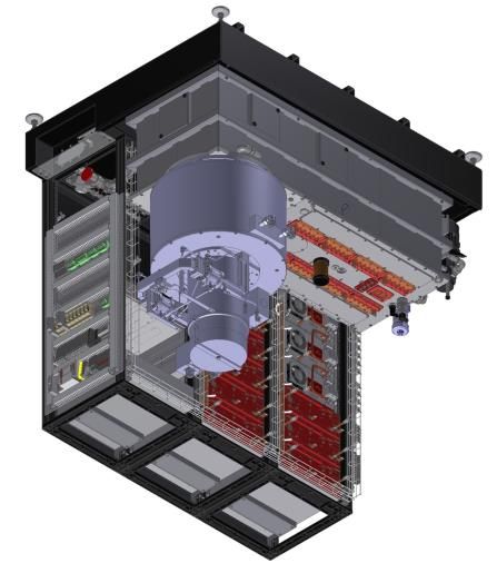
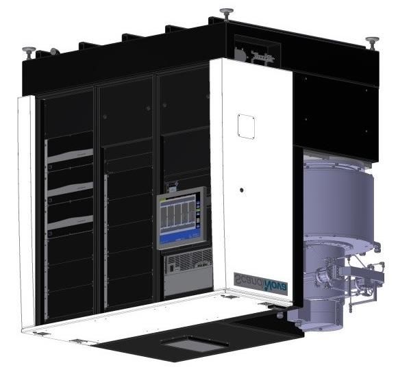
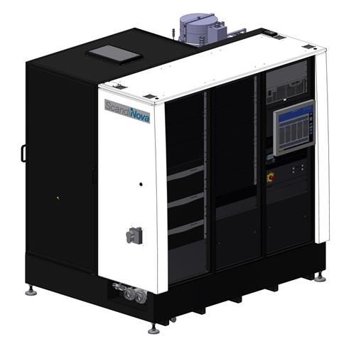
Klystron Modulator Solid State RF Amp
 Klystron

 Output Waveguide
 Solenoid Power Supply
 RF Digitizer
 Solenoid

 Local Control Unit Main Control Unit (MCU)

• The K300 is capable of producing a ~370kV, ~325A
 output pulse, 1µs in pulse length, at a repetition
 Tank
 rate of up to 100 Hz.

• The klystron modulator is an integrated stand-
 alone system, requiring only external power
 MCU SIDE
 (120VAC control power, 480VAC, 3-phase primary Dimensions (L x W x H):
 power), and water (~45gpm) for cooling. ~1.7 m x ~1.4 m x ~1.5 m

 Overall Typical Weight:
• An external source of low-lever RF power is ~4100 kg
 required to drive the solid-state amplifier/klystron.

 Klystron Modulator
 Tank Hutch Switching Units
 Filament Power Supply
 Ion Pump Controller
 Switching Units
 EMERGENCY OFF

 Power Distribution Unit (PDU)
 Capacitor Charging Supplies
 Capacitor Charging Supplies
 Main Control Unit Oil Level Sensor Main Breaker
 Klystron
 Output Waveguide
 Switching Unit Tank Connections
 AC Power
 Water
 Solenoid
 Flow Meters
 PDU SIDE
 Tank

 04/21/2021 7
Klystron

Klystron Modulator Load

 Capacitor Charging Power Supply (CCPS) Switching Unit (SU) TANK

 Pulse
 HV
 Generating HV Pulse
 Transformer
 Capacitors Transformer

 Simplified Power Circuit Topology

• The CCPS rectifies the three phase 480 VAC primary input power.
• IGBT switching is used to chop the rectified DC to drive the HV transformer primary.
• The HV transformer secondary output is rectified, and provides pulsed DC voltage to the SU.
• The SU is a high-power IGBT switching module that switches the energy stored in the
 pulse-generating capacitors as a current pulse through the primary windings of the HV pulse
 transformer.
• The HV pulse transformer provides a large step-up in voltage to deliver the required pulse
 energy to the klystron load.

 04/21/2021 8
Klystron Modulator
• Modulator: ScandiNova Model K2-2
• Klystron: Toshiba E37212
• Solenoid: Toshiba VT68954

• FAT Performance Test:
 Parameter Required Value Measured Value

 Output Pulse Voltage (kV) 366 kV 368 kV

 Output Pulse Current (A) 325 A 325 A
 Klystron Perveance (µP) 1.45 ≤ µP ≤ 1.50 1.46

 Average Power to klystron (kW) 29.9 kW

 Peak Beam Power (MW) 119.6 MW

 Pulse Top Flatness (dV) [%] within 1µs 1% 0.47%

 Pulse Repetition Rate (Hz) 100 Hz 100 Hz

 Pulse Top Length (µs) 1 µs 1 µs
 Pulse to Pulse Amplitude Stability (%) 100 ppm 48 ppm

 Voltage Pulse Rate of Rise (kV/µs) > 250 kV/µs 461 kV/µs
 Voltage Pulse Rate of Fall (kV/µs) > 250 kV/µs 393 kV/µs

 Klystron Filament DC Voltage (V) 16.2 V 17.5 V

 Klystron Filament DC Current (A) 19.2 A 19.2 A

 04/21/2021 9
Klystron Modulator
 • External Triggering
 K300

 SSA Klystron

 T1 FWD REFL
 T3
 T2
 Trigger Generator
 Fast Protect

 RF Digitizer FWD
 REFL

 T1 SSA RF ON/OFF Control

 T2 Modulator Trigger

 T3 RF Gate

Modulator
 Pulse
 0 ~2.5 5 6 Time (µs)

 04/21/2021 10
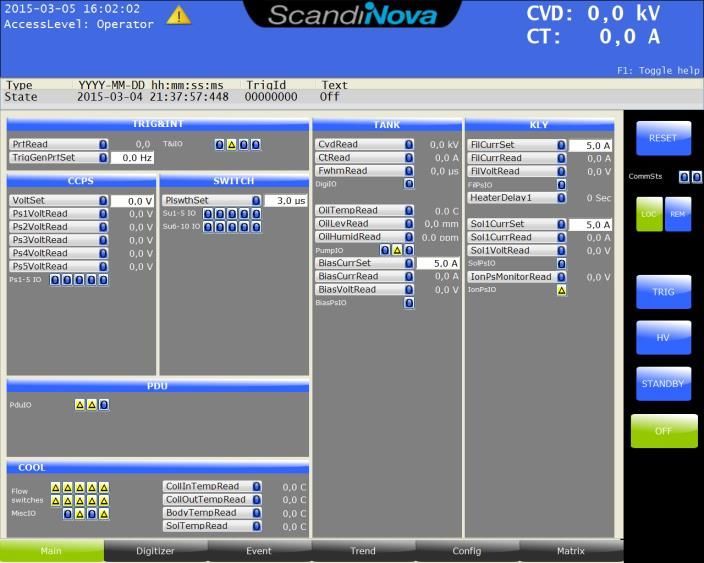
Klystron Modulator • Control system − is a PC/PLC hybrid HMI runs on Windows Typical PLC functionality, providing +24VDC control voltage and state control. − Implements a state machine that controls the transition between operational states: − Off − Standby − HV − Trigger • Main Screen − Provides local operation and summary status. • Matrix Screen − Displays the parameters and state hierarchy. 04/21/2021 11
Klystron Modulator • Digitizer Screen − Displays; Modulator voltage and current pulse samples. Forward and reflected power. VSWR RF pulse length − Digitizer implements fast protect interlock (~0.1µs) for high reflected power (using external RF switch on the LLRF source output having ~35ns switching time). • Event Screen − Running log that displays errors, warnings, interlocks and state change messages, etc.. 04/21/2021 12
Klystron Modulator/Waveguide P&ID
 BV
 ~45 gpm RTD RTD

 Supply CML 4530-02 Water Load
 ~75 psi
 FS

 Return CML 8330-04 Directional Coupler
 ~22 psi BV

 PRV
 PXIe Crate

 FR

PG PG Definitions:
 PG: Pressure Gauge
 BV: Ball Valve
BV BV Reducer Reducer FR: Flow Regulator
 2" to 1 ½ 2" to 1 ½ FI: Flow Indicator
 FS: Flow Switch
 PRV: Pressure Relief Valve
 TW: Thermal Well
 RTD: Resistance Temperature Detector
 S R
 S R K300 Klystron Modulator External Interlock
 (MCU)
 Building Water

 04/21/2021 13
Waveguide and Waveguide Components
Waveguide: WR187
 Δx
• Dimensions:
 − a = 1.872 in. (0.048 m)
 − b = 0.872 in. (0.022 m) b

 − Δx = 0.1265 in. (3.213 x 10⁻³ m)

• Material: a
 Δx
 − Copper

• Waveguide Flanges:
 − Riken-Desy type
 − Flange material; AISI-316L FWD REFL
 Water-Cooled Load
• Dielectric: E-Plane Sweep
 Water-Cooled
 Dual Directional Coupler
 − Vacuum with Pumping Port

 Klystron
 Output

• Dual Directional Coupler, Water-Cooled • Waterload
 − Coupling, FWD; 60 dB − Power Dissipation; 7.5 kW maximum average power
 − Coupling, REFL; 25 dB − VSWR; 1.10:1 maximum
 − Cooling; water (25 °C to 35 °C inlet temp.) − Cooling; water (25 °C to 35 °C inlet temp.)
 − Coolant Flow Rate; 1 gpm minimum at full power − Cooling Flow Rate: 2 gpm minimum at full power
 (~4.5 gpm in practice) (~4.5 gpm in practice)
 − Coolant Pressure; 150 psig maximum − Coolant Pressure; 150 psig maximum

 04/21/2021 14
Waveguide and Waveguide Components • Attenuation due to imperfectly conducting walls − Assumptions: Resistivity of copper at 20˚C (Wikipedia); Δx − ρres = 1.678 x 10⁻⁸ Ω m Dominant propagating mode: − TE10 b − Skin Depth at 5.712GHz; δ = 8.626 x 10⁻⁷ m a − Attenuation per unit length, α; Δx 2 3 2 2 ൬ + + ൰ 2 2 2 =0.031 dB/m = 3 ; − Power loss as a function of length; 50MW peak RF power 1µs pulse width @ 100Hz PRR 1 meter length of waveguide section ( ) = 0 −2 • Pave_loss = Ploss * Duty Cycle = 35.76 W 04/21/2021 15
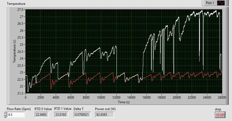
Waveguide and Waveguide Components Coefficient of Natural Convection (htot) vs Δ T • Heat Transfer Considerations (https://quickfield.com/natural_convection.htm) 25 − Assumptions: 20 Density of copper, near r.t. (Wikipedia); htot (W/m2 K) 15 − ρdensity = 8.96 x 10³ kg m-3 Specific heat capacity of copper at atmospheric pressure and near r.t. 10 (Wikipedia); 5 − cpcopper = 385 J kg-1 K-1 y = -0.079167x2 + 1.811439x + 11.425000 No power dissipated into dielectric. 0 2 0 4 6 8 10 Power dissipation per unit area in waveguide walls is uniform. ΔT (K) Consider only heat loss due to natural convection. Coefficient of natural convection calculated using online calculator (Quickfield). Convective area of waveguide; Awg = L x 2 x (ao + bo); (Awg = 0.165 m2) Initial temperature of the waveguide is equal to the ambient (air) temperature. ΔTwg vs Time Steady state application of Paveloss. 8 Paveloss=35.76W (Ppk=50MW, 1us PW, 100Hz PRR) − Energy transferred to the waveguide is given by: 7 Paveloss=17.90W (Ppk=25MW, 1us PW, 100Hz PRR) Paveloss=3.58W (Ppk=5MW, 1us PW, 100Hz PRR) 6 = න ( − ) 0 5 ΔTwg (K) = ( − ) × ∆ (k = − 1) 4 =1 3 Where; 2 × ∆ = _ × × ( − ) 1 × ∆ = ℎ × × ( − ) × ∆ 0 0 100 200 300 400 500 600 700 800 900 Time (s) 04/21/2021 16
Waveguide and Waveguide Components • Take away (my simple-minded understanding of the “conditioning” we’ve been doing): − Conditioning is more an application of peak power rather than average power. The temperature of the bulk copper is not increased significantly. − With the application of peak power, two possible mechanisms might occur: 1. Pulsed peak RF power is dissipated into the skin depth, elevating the surface temperature (“flash heating” the surface). − Contaminants adsorbed on the waveguide surface are heated and can abruptly outgas, which we observe in the vacuum. 2. Surface irregularities, such as edges, corners, particulate, can provide localized field enhancement. − The application of peak power can cause “burning” at these locations and field degradation, the energy from which may couple into the vacuum. Field breakdown would result in increased reflected power. Between RF pulses, power dissipates from the skin depth into the bulk copper of the waveguide walls, contributing to an incremental increase in the bulk copper temperature, until equilibrated with heat loss mechanisms. • Suggests an approach to conditioning: Start with reduced pulse width, low power, low rep rate. Increase power until vacuum activity is observed. Continue to “drive” vacuum activity with small increments in power, working to keep vacuum excursions below the vacuum trip threshold. After full power is obtained, gradually increase repetition rate. After full repetition rate is obtained, gradually increase pulse width. 04/21/2021 17
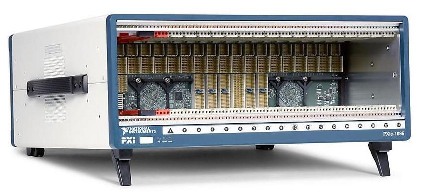
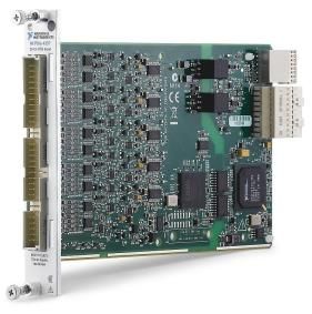
LLRF, Data Acquisition and Control
 PXIe-6341; Multifunction I/O
 • 16 SE analog inputs
 • 500 kS/s maximum sample rate
 PXIe-8840; PXI Controller • 16-bit resolution
 • Intel Core i5, 2.7 GHz dual-core processor
 • 4 counter/timers
 • 8 GB RAM
 • 24 bi-directional digital channels
 • Windows 10, 64-bit
 • 2 analog output channels
 • 2GB/s maximum controller BW
 • 900 kS/s update rate
 • LabView 2019

 PXIe-5110; Oscilloscope
 PXIe-5654; RF Analog Signal Generator
 • 2-channel, 100 MHz BW, 1 Gs/s maximum
 • 250 kHz to 10 GHz
 sample rate
 • -7 dBm to +13 dBm output power
 • -20V to +20 input voltage range
 • 8-bit analog input resolution
 • 64MB onboard memory

 PXIe-5423; Arbitrary Waveform Generator PXIe-4357; Temperature Input Module
 • 2-channel, 40MHz maximum BW • 20 channels, 100 S/s maximum sample rate
 • 800 MS/s maximum update rate • 24-bit resolution
 • 16-bit analog output resolution • 2-, 3-, 4-wire PT 100 RTD
 • -12V to 12V analog output range

 PXIe-1095; PXIe Chassis
 • 24 GB/s maximum system BW
 • 12 PXIe slots
 • 5 Hybrid slots

 04/21/2021 18
Vac-Ion Pump Vac-Ion
 K300 MCU Current Gauge

 TB??

LLRF, Data Acquisition and Control +24VDC

Original Integration Concept +24VDC

 TB??
 Flow

 12 dBm
PXIe-1095 NI-5654 max output 10 dBm K300 RTD
 AM ZFSWA2-63DR+ max input
 SSA Klystron 50 Ω

 RTD

 T1 FWD REFL
 NI-5423
 50
 T2
 T3
 40 dB 75 dB

 Fast Protect Vacuum
 Pump
 Current Pulse Sample RF Digitizer REFL Controller
 PXIe-5110 FWD FWD
 Voltage Pulse Sample FWD

 CH_5 Vacuum Ion

 50
 50
 CH_4 Gauge
 Controller
 CH_3 30 dB LB480A LB480A
 CH_2 LB480A
 CH_1
 CH_0
 PXIe-6341
 PFI_1
 PFI_0
 AI_1
 AI_0
 PXIe-4357

 RTD_inputs

 PXIe-8840
 T1

 T2

 T3

 USB
 Modulator
 Pulse
 0 ~2.5 5 6 Time (µs)

 04/21/2021 19
Vac-Ion Pump Vac-Ion
 K300 MCU Current Gauge

 Initial Conditioning Efforts
 TB??

 +24VDC

 Integration for Conditioning +24VDC

 TB??
 Flow
 12 dBm
PXIe-1095 NI-5654 max output 10 dBm K300 RTD

 ZFSWA2-63DR+ max input
 ZFSWA2-63DR+
 SSA Klystron 50 Ω

 RTD

 T1 FWD REFL
 T3 50
 T2
 40 dB 75 dB

 Fast Protect Vacuum
 Pump
 Current Pulse Sample RF Digitizer REFL Controller
 PXIe-5110 FWD FWD
 Voltage Pulse Sample FWD

 CH_5 Vacuum Ion

 50
 50
 CH_4 Gauge
 Controller
 CH_3 30 dB LB480A LB480A
 CH_2 CH3 LB480A
 CH_1 CH2 DG-645
 CH_0 CH1
 PXIe-6341

 AI_1
 AI_0

 PXIe-4357

 RTD_inputs

 PXIe-8840

 T1

 T2

 T3
 USB
 Modulator
 Pulse
 0 ~2.5 5 6 Time (µs)

 04/21/2021 20
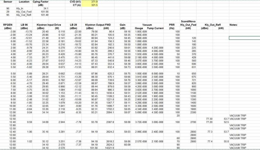
Initial Conditioning Efforts

• Conditioning began on January 30, 2020:
 − 1µs pulse width, 100 Hz PRR.
 − Klystron forward power ~90kW to ~2.6MW.
 − Observed increase in vacuum with increase in
 forward power.
 − Observed large vacuum excursions from ~2MW
 to ~2.5MW.

 Not much progress!
 04/21/2021 21
Initial Conditioning Efforts
• February 13, 2020:
 − 1µs pulse width.
 − Varied PRR from 10Hz to 150Hz.
 − Klystron forward power ~1MW to ~4.3MW.
 − Working calorimetry.
 − Large number of vacuum trips.

 04/21/2021 22
Initial Conditioning Efforts
• February 20, 2020:
 − After lunch decided to reduce pulse width to 0.4µs.
 − 100 Hz PRR.
 − Klystron forward power ~2.8MW to ~14MW.
 − Able to increase drive power while keeping vacuum
 response below vacuum trip threshold.

 Lunch
 04/21/2021 23
Initial Conditioning Efforts
• February 21, 2020:
 − Klystron forward power from ~14MW to ~50 MW,
 100Hz PRR, at pw = 0.5µs, 0.7µs, 0.8µs and 1.0µs.

 04/21/2021 24
Initial Conditioning Efforts
• Gain Curve: Klystron Output Foward Power vs Input Power FWD
 50 2000 REFL
 VDC : 1323 V
 CVD: 369.3 kV
 45 CT: 325 A 1800
 PW: 1µs
 PRR: 100 Hz
 40 1600

 35 1400
 Output FWD Power (MW)

 Output REFL Power (kW)
 30 1200

 25 1000

 20 800

 15 600

 10 400

 5 200

 0 0
 0 20 40 60 80 100 120
 Input Power (W)
 Modulator: K2-2, SN LANL
 Klystron: E37212, SN 15M004
 Solenoid: VT68954, SN 15L035

 04/21/2021 25
Conclusions

• Klystron/modulator is a compact, well-integrated system.
• LLRF, data acquisition/control system still a work in progress
• USB-based power sensors proved problematic, recommend using calibrated
 diode detection for forward and reflected power measurements.
• Gaining valuable conditioning experience as the system continues to
 expand.

 04/21/2021 26
Back Up Excel spreadsheet calculates ΔTwg by successive substitution. = න ( − ) 0 = ( − ) × ∆ ( = − 1) (Approximation) =1 ∆ = ∆ − ∆ k ∆ = × ∆ = _ × × ( − ) ∆ = × ∆ = ℎ × × ( − ) × ∆ = ∆ − ∆ − = _ × 04/21/2021 27
Back Up • Linear expansion of copper: − α = 17µm m-1 K-1 (Wikipedia) For: − length of waveguide, L = 1 m, − and ΔTwg = 5 °C; ∆ = × ∗ ∆ = 85 04/21/2021 28
You can also read