The State-of-the-Art of Smartphone Imagers
←
→
Page content transcription
If your browser does not render page correctly, please read the page content below
R01
The State-of-the-Art of Smartphone Imagers
Ray Fontaine, TechInsights Inc., 1891 Robertson Road, Suite 500, Ottawa, ON K2H 5B7, Canada,
Phone: 1-877-826-4447, Email: rfontaine@techinsights.com
functionality required to support the popular full-chip
Abstract— The smartphone imaging ecosystem is well dual photodiode PDAF systems.
into the “imaging plus” era. Advanced chip stacking
techniques have enabled new functionality, including multi-
frame noise reduction, slow-motion video, and other
advanced image signal processing features. Pixel-level
interconnect has been successfully demonstrated and is
coming soon to mass-produced CMOS image sensors (CIS).
Active pixel arrays, including the latest
0.8 µm pixel generation, are now commonly augmented
with specialized phase detection autofocus (PDAF) pixels.
The rise of 2x1 on-chip lens (OCL) structures has been
noted in sub-micron pixels as an enabler for lossless PDAF.
Flagship smartphones now employ multiple camera
systems, with each camera in the ecosystem customized per
use case. The multi-cam approach is driving improved
image quality, and the trend to include companion time-of-
flight (ToF) cameras is enabling new feature sets to assist Fig. 1 Smartphone Rear-Facing Camera ISP Die Size (2013-2019)
these advanced imaging systems.
As for chip-to-chip interconnect in two-die stacked
I. INTRODUCTION imagers, peripheral through silicon via (TSV) arrays are
S
still in wide use. TSMC continues to hold the record for
martphones continue to be the preferred camera
smallest known imager TSV pitch at 4.0 µm, first
systems of most consumers to the extent that the once
documented in a 16 MP, 1.0 µm generation OmniVision
popular compact digital camera market has substantially imager in 2016. Hybrid bonding is gradually emerging as
shrunk and the digital single lens reflex (DSLR) and a TSV array replacement, and the current record for
mirrorless camera markets have been largely relegated to known production hybrid bonding pad pitch is held by
hobbyist status. Image quality across all application Sony for 1.5 µm wide, 3.1 µm pitch interconnect pads in
segments continues to improve. In 2015, the trend for its 48 MP, 0.8 µm generation imager. TSMC-fabricated
smartphone primary camera resolution split in two: one imagers with hybrid bonding were first documented in
preference was optimization of the 12 MP class sensors mass produced imagers in 2017 and featured 3.6 µm pitch
(Apple, Google, Samsung Galaxy, etc.), while the hybrid bonding pads (Fig. 2). While pixel-level
megapixel race continued from 16 MP, to 20 MP and interconnect has been demonstrated in small-pixel
currently into the 48 MP generation. imagers and sensors [1,2], this architecture has not yet
been found to be in downstream products.
II. CHIP STACKING, CHIP-TO-CHIP INTERCONNECT
Most smartphone rear-facing cameras require two-die
stacked imagers. The use of TSMC’s 40 nm generation
image signal processors (ISPs) is widespread, whereas
Samsung continues to use 28 HKMG for premium ISPs
and 65 nm for general use. The observed trend for rear-
facing camera stacked imager ISPs (Fig. 1), shows a
decrease in die area for most popular resolutions. In the
case of 12 MP stacked imagers, the trend of increasing
ISP chip area is most likely attributed to added Fig. 2 Observed Min. Imager Hybrid Bonding Pitch (l), TSV Pitch (r)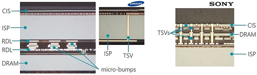
In 2018, Samsung and Sony successfully deployed IV. SUBSTRATES AND DEEP TRENCH ISOLATION
triple-stacked imagers in the Galaxy S9 (Fig. 3). The As pixels shrink, thicker active Si is required to
Samsung solution employed a flip-chip strategy where a maintain a suitable photodiode size. From the
DRAM die with redistribution layer (RDL) was
introduction of back-illuminated imagers in smartphones
connected to the back of a two-die stacked imager ISP
the active Si thickness had tended to be in the range of
RDL through micro-bumps. High aspect ratio, Cu-filled
2.5 µm to 3.0 µm for Sony and Samsung fabricated
TSVs connect the ISP back RDL to the front ISP
metallization. The Sony variant featured a 2nd generation imagers and 3.5 µm active Si is in use in the latest
Samsung solution would seem to offer more integration sub-micron pixels. The state-of-the-art for the 0.8 µm
flexibility as it uses a commodity DRAM. pixel generation active Si is 3.6 µm from Sony and
3.7 µm for Samsung. Fig. 4 summarizes the general
correlation between pixel pitch and active Si thickness in
smartphone imagers.
Fig. 3 Samsung (l), Sony (r) Triple Stacked Imagers
III. PIXEL SCALING
Pixel scaling has continued down to the current 0.8 µm
generation. Table 1 illustrates the additional
development time needed to bring the 1.12 µm, 1.0 µm
and 0.9 µm generations to mass production.
Pixel Pitch Vendor Year of Mass Time to
(µm) Production Introduction Fig. 5 Smartphone Imager Active Si Thickness vs. Pixel Pitch (2009-
2.2 Micron 2006 not analyzed 2019)
1.75 Micron 2007 ~1 yr.
1.4 Sony 2008 ~1 yr. A key technology enabler for thicker active Si is DTI
1.12 Sony 2011 ~3 yr.
1.0 Samsung 2015 ~4 yr.
and associated high-k defect passivation films. Front-
0.9 Samsung 2018 ~3 yr. DTI is in use by Samsung at the 0.8 µm, 0.9 µm and
0.8 Sony 2019 ~1 yr. 1.0 µm generations and requires the use of vertical
Table 1: Major Pixel Generation Introduction transfer gates (VTG). Samsung uses back-DTI and planar
transfer gates for larger pixel sizes. All other vendors and
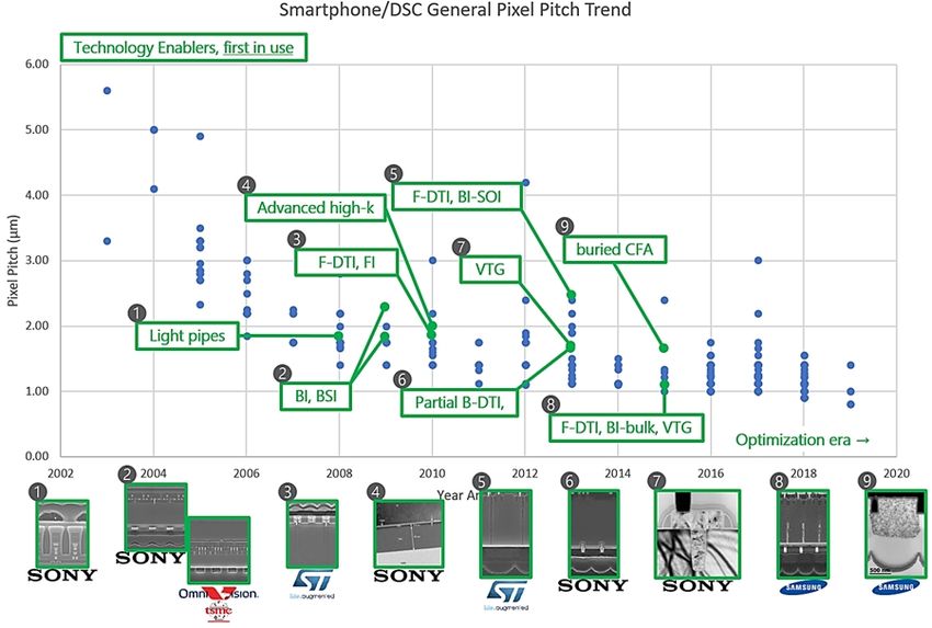
Fig. 4 illustrates the introduction timeline of selected foundries prefer back-DTI for small pixel isolation. The
technology elements that have enabled small pixel introduction of various DTI schemes is the last major
scaling. structural development for small-pixel imagers, and the
application space has been in a period of incremental
evolution and optimization for the last few years.
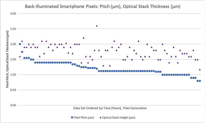
V. OPTICAL STACKS
The shrinking pixel trend has loosely correlated to
thinner back-of-Si optical stacks (on-chip lens, color
filter, pre-metal dielectric, high-k film). The thinning
tends to come primarily through burying the color filters
in the metal grid, however optical stack thinning is not
necessarily associated with pixel scaling. Some vendors
have invested in advanced light pipe development
yielding improved performance but with a net thicker
Fig. 4 Small-Pixel Scaling Enablers optical stack. Fig. 6 is a survey of smartphone rear-facing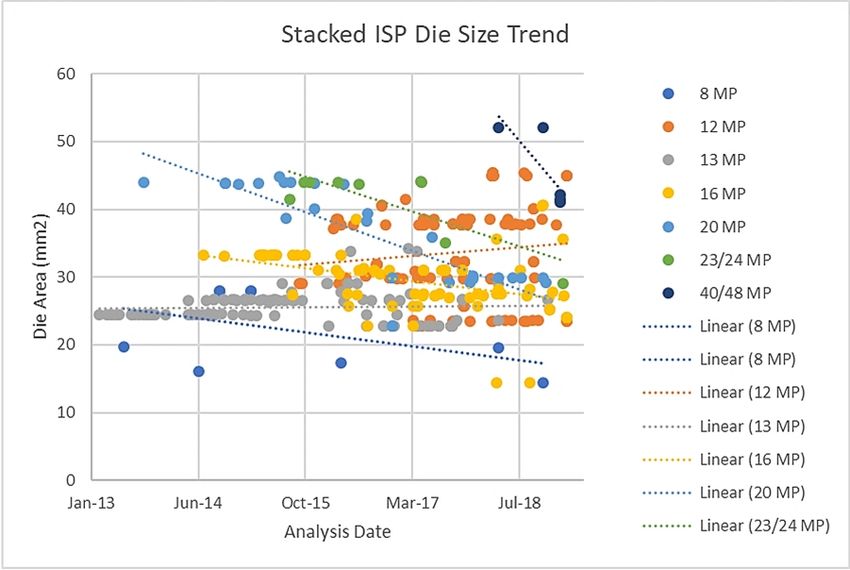
camera optical stack thickness and pixel generation. The              Masked PDAF pixel systems were originally deployed
record thin optical stack is 1.2 µm for Samsung’s 0.8 µm           in smartphone active pixel arrays in 2014 and continue to
pixel generation.                                                  be the dominant solution in use. Masked PDAF pixels
   Bayer RGB color filter array (CFA) use dominates                have been successfully deployed in 1.55 µm down to
smartphone imagers, although a 2x2 pixel-per-color filter          1.0 µm generation pixels. Fig. 8 shows the masked PDAF
strategy has emerged as a solution for high dynamic                Samsung has used in its 0.8 µm generation pixels
range (HDR) and low light imaging. Huawei recently                 featuring Tetracell CFA and ISOCELL Plus [4]
introduced a RYYB sensor in its P30 series [3], which              technology. In this case, the 0.8 µm generation pixels are
may stimulate the reintroduction of non-Bayer CFAs.                binned to an effective 1.6 µm pitch pixel and each PDAF
                                                                   photosite is half-masked and uses a clear filter.

                                                                   Fig. 8 Samsung Masked PDAF (Tetracell CFA, Grid, ISOCELL Plus
                                                                   Cross-Section)

                                                                      Dual photodiode is a popular solution for 1.4 µm
                                                                   generation pixels and Samsung has extended
                                                                   development of dual photodiode PDAF down to the
Fig. 6 Optical Stack Thickness, Pixel Pitch (2009-2019)            1.28 µm generation claiming use of the world’s smallest
                                                                   photodiodes [5]. Dual photodiodes are not currently
                           VI. PDAF                                expected to be developed for sub-micron pixels. Instead,
  Smartphone camera developers are constantly pushed               2x1 OCL has emerged as a solution for the smallest of
to improve autofocus system speed and performance,                 pixels and is in use for the 1.22 µm to 0.8 µm pixel
particularly in low light conditions. Masked, dual                 generations. Fig. 9 shows the latest 2x1 OCL structures
photodiode, and 2x1 OCL PDAF are all in use in                     in Sony’s current 0.8 µm generation pixels.
smartphone imagers. Multi-camera systems often use a
combination of PDAF systems, each specialized for use
case and pixel size. Fig. 7 summarizes the smartphone
PDAF system insertion timeline by pixel generation.

                                                                   Fig. 9 Sony 2x1 OCL PDAF (Quad Bayer CFA, Tilt, Planar, Cross-
                                                                   Section)

                                                                                            REFERENCES
                                                                              [1]   Venezia, et al. “1.5µm Dual Conversion Gain,
                                                                                    Backside Illuminated Image Sensor Using Stacked
                                                                                    Pixel Level Connections with 13ke- Full-Well
                                                                                    Capacitance and 0.8e- Noise”, IEDM 2018
                                                                              [2]   Jourdan, et al. “Hybrid bonding for 3D stacked
                                                                                    image sensors: impact of pitch shrinkage on
                                                                                    interconnect robustness”, IEDM 2018
                                                                              [3]   “Huawei Rewrites the Rules of Photography with
                                                                                    Groundbreaking HUAWEI P30 Series”, Huawei
                                                                                    Press Release, March 26, 2019
                                                                              [4]   “Samsung Brings Enhanced Color Accuracy and
                                                                                    Sharpness to Mobile Photos with New ISOCELL Plus
                                                                                    Technology”, Samsung Press Release, June 27, 2018
                                                                              [5]   Choi, et al. “An All Pixel PDAF CMOS Image Sensor
                                                                                    with 0.64μm×1.28μm Photodiode Separated by Self-
                                                                                    aligned In-pixel Deep Trench Isolation for High AF
                                                                                    Performance”, VLSI 2017

Fig. 7 Smartphone PDAF Use: Masked (t), Dual PD (c), 2x1 OCL (b)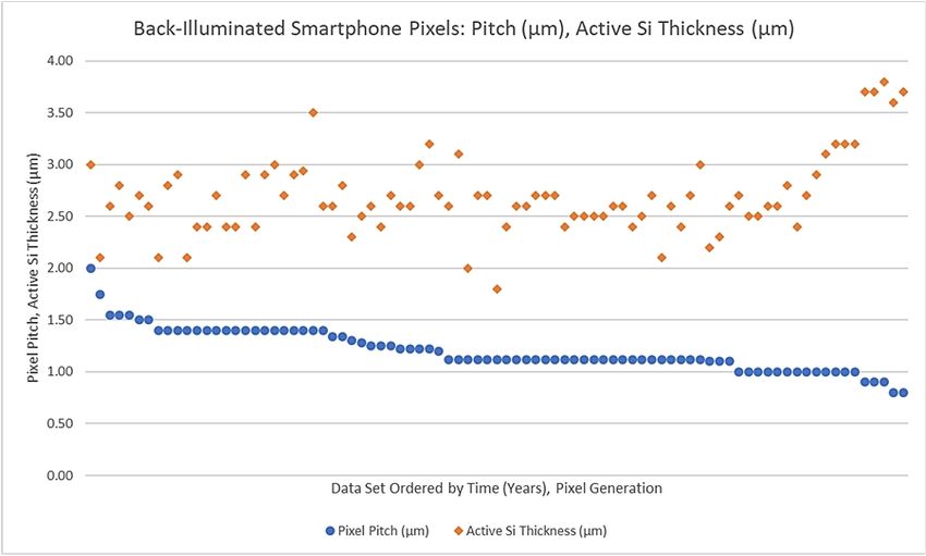
You can also read