Nanoscale compositional evolution in complex oxide based resistive memories
←
→
Page content transcription
If your browser does not render page correctly, please read the page content below
Nanoscale compositional evolution in complex
                                                     oxide based resistive memories
                                                     TAIMUR A HMED , 1,* S UMEET WALIA , 1 E DWIN L. H. M AYES , 2 R AJESH
                                                     R AMANATHAN , 3 PAUL G UAGLIARDO, 4 V IPUL B ANSAL , 3 M ADHU
                                                     B HASKARAN , 1 J. J OSHUA YANG , 5 AND S HARATH S RIRAM 1
arXiv:1807.00185v1 [cond-mat.mtrl-sci] 30 Jun 2018

                                                     1 Functional  Materials and Microsystems Research Group and Micro Nano Research Facility, RMIT
                                                     University, Melbourne, VIC 3001, Australia
                                                     2 RMIT Microscopy and Microanalysis Facility, RMIT University, Melbourne, VIC 3001, Australia
                                                     3 Ian Potter NanoBioSensing Facility, NanoBiotechnology Research Laboratory, School of Science, RMIT
                                                     University, Melbourne, VIC 3001, Australia
                                                     4 Centre for Microscopy, Characterisation and Analysis, The University of Western Australia, Perth, WA
                                                     6009, Australia
                                                     5 Department of Electrical and Computer Engineering, University of Massachusetts, Amherst, MA 01003,
                                                     USA
                                                     * taimur.ahmed@rmit.edu.au

                                                     Abstract: Functional oxides based resistive memories are recognized as potential candidate
                                                     for the next-generation high density data storage and neuromorphic applications. Fundamental
                                                     understanding of the compositional changes in the functional oxides is required to tune the
                                                     resistive switching characteristics for enhanced memory performance. Herein, we present the
                                                     micro/nano-structural and compositional changes induced in a resistive oxide memory during
                                                     resistive switching. Oxygen deficient amorphous chromium doped strontium titanate (Cr:a-
                                                     SrTiO3−x ) based resistance change memories are fabricated in a Ti/Cr:a-SrTiO3−x heterostructure
                                                     and subjected to different biasing conditions to set memory states. Transmission electron
                                                     microscope based cross-sectional analyses of the memory devices in different memory states
                                                     shows that the micro/nano-structural changes in amorphous complex oxide and associated redox
                                                     processes define the resistive switching behavior. These experimental results provide insights
                                                     and supporting material for Ref. [1].

                                                     Introduction
                                                     In recent years, a variety of materials exhibiting resistive switching behavior, such as binary metal
                                                     oxides and transition metal oxides, have been reported. Strontium titanate, a model perovskite
                                                     oxide system, has shown significant potential for valance change resistive switching memories
                                                     owing to its tunable defect chemistry via doping, mixed anionic-electronic and non-linear
                                                     switching dynamics [2–5]. Despite enormous characterization efforts, the driving nanoscale
                                                     redox processes and associated micro/nano compositional changes in the oxide system are still
                                                     not completely clear. Here, we utilize different cross-sectional transmission electron microscope
                                                     (TEM) analyses techniques, such as energy dispersive x-ray spectroscopy (EDS) and electron
                                                     energy loss spectroscopy (EELS), to study the effect of biasing conditions and device structure
                                                     on the resistive switching behavior in Ti/Cr:a-STOx based memory cells. The micro-structural
                                                     analyses shows that top Ti layer introduces a Ti2 O3 interfacial layer with Cr:a-STOx and acts
                                                     as an oxygen reservoir during redox processes. Furthermore, formation of oxygen deficient
                                                     filamentary paths at locally crystalline regions of Cr:a-STOx control the resistive switching
                                                     behavior. These results provide supporting material for our recent report on inducing different
                                                     resistive switching behaviors in Cr:a-STOx based resistive memories [1].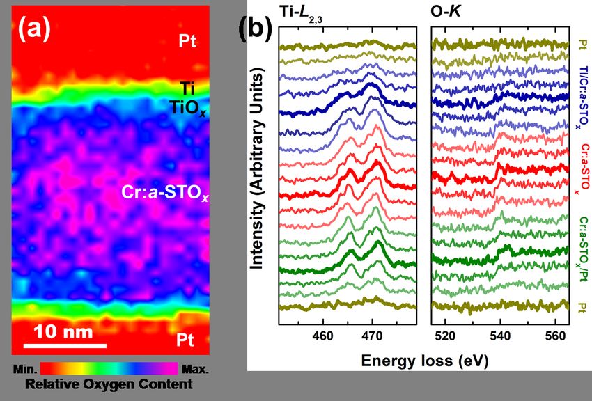
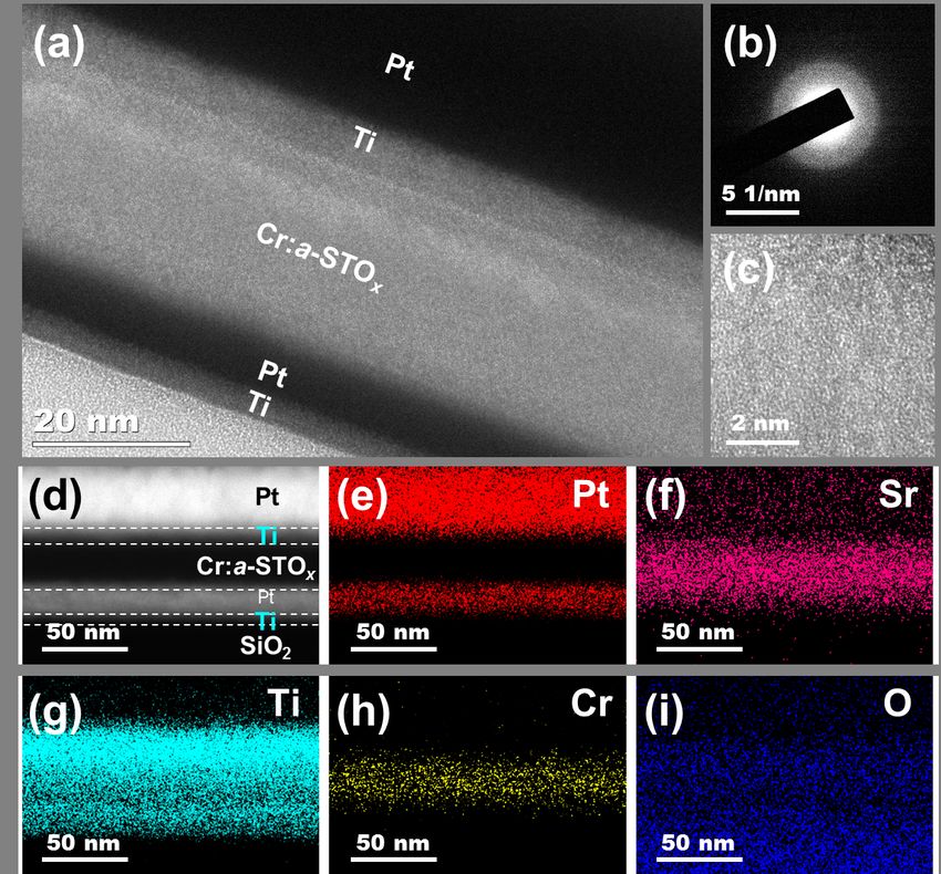
Results
The memory devices are fabricated in metal-insulator-metal (MIM) configuration by following
the fabrication steps in Ref. [1] on SiO2 /Si substrates. In the MIM structure Pt (35 nm)/Ti (8 nm)
serves as a top metal electrode, Cr:a-STOx (25 nm) as an insulator and Pt (7 nm)/Ti (3 nm) as a
bottom metal electrode. In order to ascertain the effect of applied bias (during electroforming and
resistive switching) on the metal/oxide interfaces and within the functional oxide (Cr:a-STOx ),
the cross-sectional TEM lamellae are prepared via focused ion beam (FIB) cuts from separate
MIM memory cells subjected to different biasing conditions namely; pristine, electroformed
and switching devices. The cross-sectional TEM and EDS analyses of a pristine Cr:a-STOx
MIM device is presented in Fig 1. The TEM micrograph (Fig. 1a) of the MIM structure shows
the Cr:a-STOx oxide film is sandwiched between the top Pt/Ti and bottom Pt electrodes. The
selected-area electron diffraction (SAED) pattern (Fig. 1b) and high-resolution TEM (HRTEM)
micrograph (Fig. 1c), collected from the MIM cross-section show an amorphous structure of the
Cr:a-STOx oxide film. Fig. 1d shows a high-angle annular dark field (HAADF) micrograph
of the pristine cross-section in scanning TEM. Fig.1(e−i) present elemental EDS maps of Pt,
Sr, Ti, Cr and O, respectively. The EDS maps confirm successful Cr doping in the a-STOx (via
co-sputtering of Cr and a-STO3 ) and also the desired MIM structure of the memristive devices to
execute multiple resistive switching behaviors.

   The electronic composition and the relative distribution of oxygen content across the pristine
MIM device is presented in the EELS area map (Fig. 2a), collected by considering the O−K
edge intensities. The EELS Ti−L2,3 and O−K edge profiles (Fig. 2b) are also obtained from
a line-scan across the MIM structure. Broad Ti−L3 and Ti−L2 peaks at the top Ti/Cr:a-STOx
interface can be used to identify the oxidation states of Ti (i.e., presence of mixed Ti2+ and Ti3+
oxidation states at the top interface) as explained in Ref [6].

   The electroforming of Cr:a-STOx MIM devices is carried out by applying a negative voltage
(
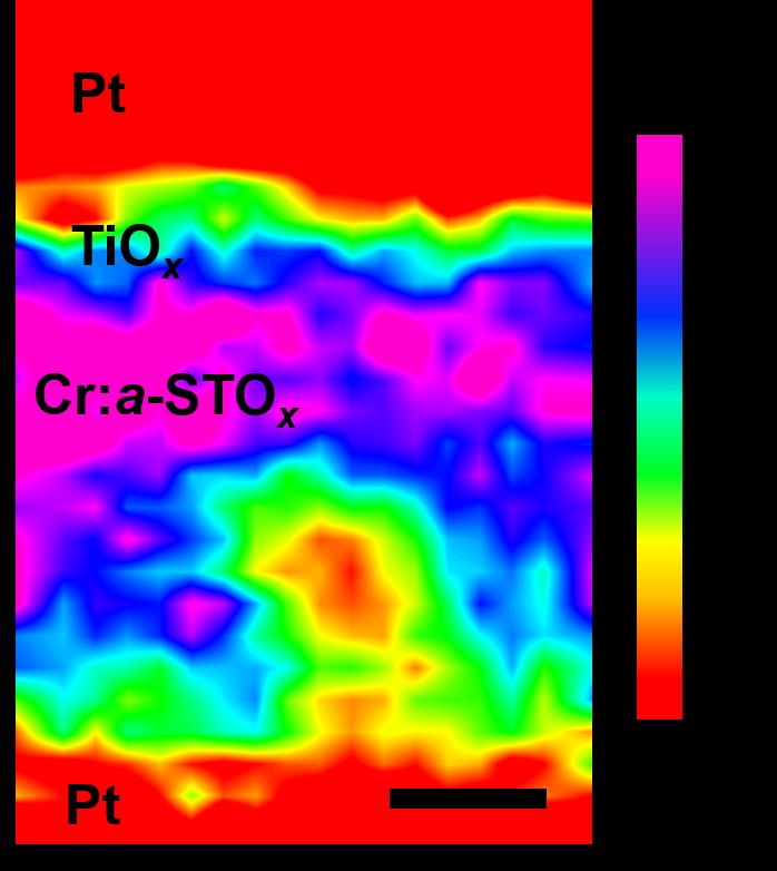
Å) is used to generate the iFFT (Fig. 5c) highlighting the presence of [011] cubic STO phase in
the selected ROI.

   Fig. 6 shows the EELS O−K edge area map of the locally crystalline ROI from the MIM
device exhibiting CW-BP resistive switching behavior (presented in Fig. 5). The representative
MIM device is set to HRS prior to TEM sample preparation. Relatively low oxygen content at the
bottom Pt electrode shows a ruptured filamentary path and accumulation of the Vo s at anode in
HRS. Presence of varying oxygen content at the vicinity of top Pt electrode shows the oxidation
of Ti layer to a sub-stoichiometric Ti2 O3 , as indexed in the FFT analysis (as presented in Fig. 4).

Acknowledgments
The authors acknowledge support from the Australian Research Council (ARC) for personnel
and project support via DP130100062 (S.S.), DE160100023 (M.B.), and FT140101285 (V.B.)
and equipment funding through LE0882246, LE0989615, LE110100223, and LE150100001.
The authors would like to acknowledge the technical assistance of the Micro Nano Research
Facility (MNRF) and the RMIT Microscopy and Microanalysis Research Facility (RMMF). Also
Australian Microscopy and Microanalysis Research Facility, AuScope, the Science and Industry
Endowment Fund, and the State Government of Western Australian for contributing to the Ion
Probe Facility at the Centre for Microscopy, Characterisation and Analysis at the University of
Western Australia.

References
1. T. Ahmed, S. Walia, E. L. H. Mayes, R. Ramanathan, P. Guagliardo, V. Bansal, M. Bhaskaran, J. J. Yang, and
   S. Sriram, “Inducing tunable switching behavior in a single memristor,” Appl. Mater. Today 11, 280–290 (2018).
2. H. Nili, S. Walia, A. E. Kandjani, R. Ramanathan, P. Gutruf, T. Ahmed, S. Balendhran, V. Bansal, D. B. Strukov,
   O. Kavehei, M. Bhaskaran, and S. Sriram, “Donor-induced performance tuning of amorphous SrTiO3 memristive
   nanodevices: Multistate resistive switching and mechanical tunability,” Adv. Func. Mater. 25, 3172–3182 (2015).
3. H. Nili, T. Ahmed, S. Walia, R. Ramanathan, A. E. Kandjani, S. Rubanov, J. Kim, O. Kavehei, V. Bansal, M. Bhaskaran,
   and S. Sriram, “Microstructure and dynamics of vacancy-induced nanofilamentary switching network in donor doped
   SrTiO3 − x memristors,” Nanotechnology 27, 505210 (2016).
4. T. Ahmed, S. Walia, E. Mayes, R. Ramanathan, V. Bansal, M. Bhaskaran, S. Sriram, and O. Kavehei, “High order
   synaptic learning in neuro-mimicking resistive memories,” (2018). 44 pages, 11 figures.
5. T. Ahmed, S. Walia, J. Kim, H. Nili, R. Ramanathan, E. L. H. Mayes, D. Lau, O. Kavehei, V. Bansal, M. Bhaskaran, and
   S. Sriram, “Transparent amorphous strontium titanate resistive memories with transient photo-response,” Nanoscale
   9, 14690–702 (2017).
6. Y. Li, Q. Wang, M. An, K. Li, N. Wehbe, Q. Zhang, S. Dong, and T. Wu, “Nanoscale chemical and valence evolution
   at the metal/oxide interface: A case study of Ti/SrTiO3 ,” Adv. Mater. Interf. 3, 1600201 (2016).
Fig. 1. Microstructure structure of the pristine Cr:a-STO x devices. (a) TEM micrograph
of a pristine MIM device. (b) Selected area electron diffraction pattern collected from the
MIM cross-section. (c) High resolution TEM micrograph of the Cr:a-STO x oxide film. (d)
High-angle annular dark field TEM micrograph of the pristine MIM device.The elemental
EDS mapping of (e) Pt, (f) Sr, (g) Ti, (h) Cr and (i) O.

Fig. 2. Electronic structure of the pristine Cr:a-STO x devices. (a) The EELS O−K edge
area map and (b) the EELS Ti−L2,3 and O−K edge profiles along a line scan across the MIM
device
Fig. 3. Morphological analyses of electroformed devices. (a) TEM micrograph of the MIM
device subjected to electroforming step. The box encloses the ROI. (b) The FFT diffraction
patterns generated from the ROI enclosed in (a). (c) The iFFT obtained from a diffraction
spot in (b) highlight the crystalline region along the bottom electrode.

Fig. 4. Micro-structure of top Pt/Ti/Cr:a-STO x interface of electroformed MIM devices.
(a) TEM micrograph of top interface. Two ROIs are selected at Location 1 and Location 2,
enclosed in boxes. Scale bar denotes 10 nm. (b) and (c) are the FFT diffraction patterns
generated from Location 1 and Location 2, respectively, in (a).
Fig. 5. Morphological analyses of the Cr:a-STO x MIM devices in HRS and exhibiting
CW-BP resistive switching behavior. (a) TEM micrograph of the MIM device subjected to
at least 100 resistive switching cycles and set to HRS prior to the lamella preparation. ROI
is enclosed in the box. Scale bars 5 nm. (b) The FFT diffraction patterns generated from the
ROI enclosed in (a). (c) The iFFT obtained from spot 1 in (b) highlight the crystalline region
Fig. 6. The EELS O−K edge area map of the raptured conductive filamentary path in HRS.
Scale bar represents 20 nm.
You can also read