ULSI and TFT technologies in industry, research and higher education in France: An evolution towards innovation resulting from close and ...
←
→
Page content transcription
If your browser does not render page correctly, please read the page content below

Engineering Conferences International
ECI Digital Archives
Semiconductor Technology for Ultra Large Scale
                                                                                Proceedings
Integrated Circuits and Thin Film Transistors VII

5-20-2019

ULSI and TFT technologies in industry, research
and higher education in France: An evolution
towards innovation resulting from close and
sustainable interaction
Olivier Bonnaud

Follow this and additional works at: https://dc.engconfintl.org/ulsic_tft_vii
   Part of the Semiconductor and Optical Materials Commons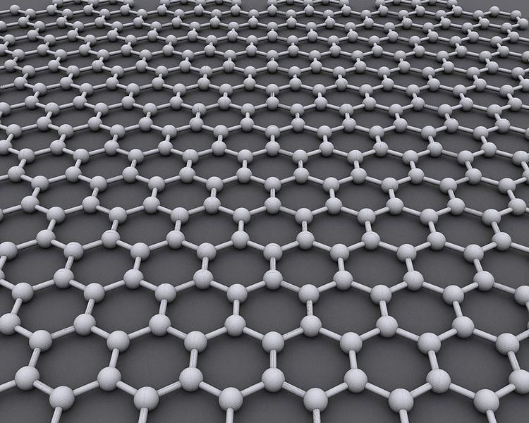
TITRE
INSTITUT D’ÉLECTRONIQUE ET DE TÉLÉCOMMUNICATIONS DE RENNES

                           ULSI and Thin Film Semiconductor Technologies:
                             Evolution of Industry and Research Linked to
                                       Higher Education in France
                              Semiconductor Technology for Ultra Large Scale
                              Integrated Circuits and Thin Film Transistors VII
                                                             May 19-23, 2019 - Kyoto, Japan
                                                                                       Prof. O. Bonnaud,
                                                                              Executive Director of GIP-CNFM

                                  GIP-CNFM: National Coordination for Education in Microelectronics and nanotechnologies
                                  Département Microélectronique et Capteurs - IETR, Université de Rennes I,
                                  olivier.bonnaud@univ-rennes1.fr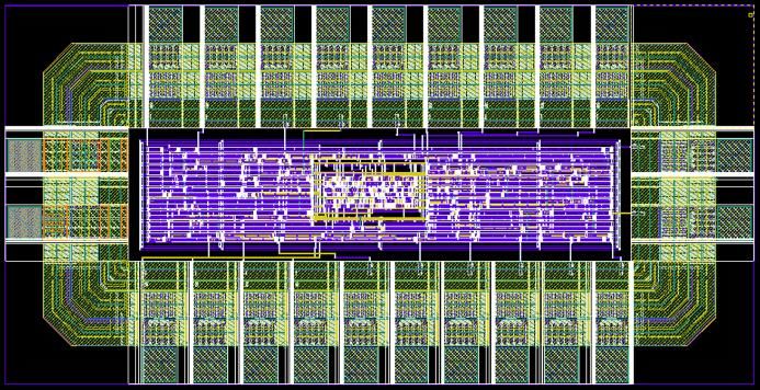
Introduction

               The microelectronics: a long term national strategy
          The evolution of microelectronics in France was linked to a very strong
          effort of the French government in 80’s.
          More recently, a new national plan was engaged by the French government
          with the goal to answer to the evolution towards connecting objects,
          Internet of Things, and Industry 4.0.
          Thus, this plan wants to boost the national activities in the large area
          technologies and the IC’s in order to meet the new needs and the related
          challenges.
          Both aspects are considered:
          - The technological challenges in terms of integration, flow of data,
            broadening of application domains, and energy consumption
          - The human challenges in terms of the higher education that guarantee a
            minimum of know-how to overpass the technological challenges: high
            skills in the field and multidisciplinary adaptability.

                                                                              2/38
O. Bonnaud, ULSI vs TFT, Kyoto (Japan), 19 – 23 May, 2019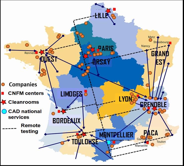
Outline

               Introduction

               ULSI &TFT technologies: common evolutions

               New challenges towards IoT and connected objects

               Needs of a National Microelectronics education network

               Challenges on the training of engineers and doctors

               Conclusion

                                                                     3/38
O. Bonnaud, ULSI vs TFT, Kyoto (Japan), 19 – 23 May, 2019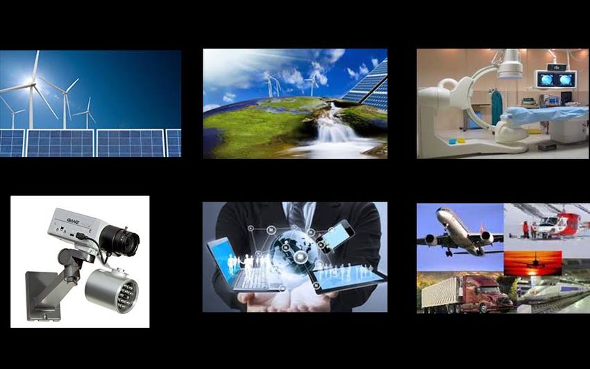
Outline

               Introduction

               ULSI &TFT technologies: common evolutions

               New challenges towards IoT and connected objects

               Needs of a National Microelectronics education network

               Challenges on the training of engineers and doctors

               Conclusion

                                                                     4/38
O. Bonnaud, ULSI vs TFT, Kyoto (Japan), 19 – 23 May, 2019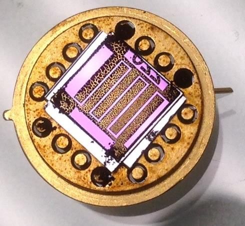
ULSI &TFT technologies: common evolutions

                ULSI technologies: continuous integration increase

                                                                                     MemFlash3D_48dies
                                                                                            10Tb
                                                                                        Prototype 2015

       2015

 2.1 bn transistors

       1963

    4 transistors

                      After G.E. Moore, Electronics Magazine, 38 (8), pp.114-117 (1965)
                      After M. Swaminathan, J.M. Pettit, 3rd System Integration Workshop (2011).

       The integration was governed by the decreasing of the minimum size of
       elementary device based on self-organization control, till at atomic scale.

                                                                                                   5/38
O. Bonnaud, ULSI vs TFT, Kyoto (Japan), 19 – 23 May, 2019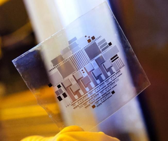
ULSI &TFT technologies: common evolutions

                         Main approaches of ULSI technologies
       The main goal is to reach high electrical properties of the final devices or
       circuits

       These approaches are very close to the TFTT ones! Many topics are common,
       more especially the low temperature process steps and thermal treatments.
                                                                              6/38
O. Bonnaud, ULSI vs TFT, Kyoto (Japan), 19 – 23 May, 2019
ULSI &TFT technologies: common evolutions

                          Main approaches of TFT technologies
       The main approaches of thin film transistors technologies are very close to
       ULSI ones : high electrical properties of the final devices or circuits

                                                                             7/38
O. Bonnaud, ULSI vs TFT, Kyoto (Japan), 19 – 23 May, 2019
ULSI &TFT technologies: common evolutions
Main approaches of TFT technologies
Example of evolution of thin film transistors: from polySi transistors to
sensors, 3D and new materials for flexible applications
Laser Pulsed Laser TFT
10
-4 VDS=1V crystallization S 10-3 VDS=1V
//
SPC PolySi TFT
Drain Current (A)
10-5 µ= 510 cm²/V.s
-6
gb
IDS (A)
10
Drain Polysilicon IDS 10-7
-8
µ = 290 cm²/V.s
10 10-9
10-11
10
- 10
-20 -10 0 10 20 30
D -20 -10 0 10 20
VGS(V)
Gate Voltage (V)
Magnetic TFT sensor Suspended Gate TFT Vertical TFT Flexible TFT
Drain
D G S
Source
Hall contact
After L. Pichon et al. Solid State After F. Bendriaa, et al., ECS After P. ZHANG, et al. Solid-State
Electronics, 38(8), 1515-1521 (1995) Vol. 2004-15, (2005), pp.284-288 Electronics, Vol. 86, 1-5, Aug. 2013
8/38
O. Bonnaud, ULSI vs TFT, Kyoto (Japan), 19 – 23 May, 2019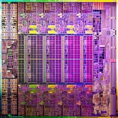
ULSI &TFT technologies: common evolutions

                              New processes for TFT circuits

   E. G. Bittle, et al." Nature Communications 7,           Chuan Wang et al. Nano Letters
      Article number: 10908, March 10, 2016                 12(3):1527-33 · February 2012

       Flexible substrates, organic semiconductors, room temperature processes,
       and printed technics are the main breakthroughs in thin film technologies.

                                                                                             9/38
O. Bonnaud, ULSI vs TFT, Kyoto (Japan), 19 – 23 May, 2019
ULSI &TFT technologies: common evolutions
Common needs: third dimension
Examples of ULSI and TFT technologies with vertical conductions.
ULSI TFT
FinFET
VTFT
After J.P. Colinge, Microelectronic After P. Zhang, et al., ECS Trans. 50(8), 59-64 (2012)
Engineering 84, 2071-2076 (2007)
10/38
O. Bonnaud, ULSI vs TFT, Kyoto (Japan), 19 – 23 May, 2019ULSI &TFT technologies: common evolutions
Convergence of both technologies
Integration of circuits and systems
1012 106
Moore's law
1010 105
System components density /cm2
Components/cm2
Transistors per die
104
108 IoT
103
106 Moore’s world
102
104 SiP 101
102 SoC
100
More than Moore’s
100
1960 1965 1970 1975 1980 1985 1990 1995 2000 2005 2010 2015 2020
Year
The new integration for IoT includes SIP and SOC, and thus involves ULSI
and TFT techniques and technologies.
11/38
O. Bonnaud, ULSI vs TFT, Kyoto (Japan), 19 – 23 May, 2019Outline
Introduction
ULSI &TFT technologies: common evolutions
New challenges towards IoT and connected objects
Needs of a National Microelectronics education network
Challenges on the training of engineers and doctors
Conclusion
12/38
O. Bonnaud, ULSI vs TFT, Kyoto (Japan), 19 – 23 May, 2019New challenges towards IoT and connected objects
Principle of the connecting objects: new technologies
A connected object includes sensors, actuators, signal processing, emission,
reception, energy harvesting, and displays, alarms, controls ...
Connected object combines large area electronics (LAE) and ultra-large
integrated electronics (ULSI). A large spectrum of knowledge!
LAE (TFT) & ULSI ULSI LAE (TFT) & ULSI
Component on site Communications Remote
TFT ULSI GSM, Wifi Monitoring
Bluetooth Data center
Energy Zigbee
harvesting Displays Alarms Control 3G-4G-5G, Displays
TNT
Sensors Signal Emission Emission
processing
Actuators Reception Reception
After O. Bonnaud et al., ICATI’2016, Bali (Indonesia), July 2016
13/38
O. Bonnaud, ULSI vs TFT, Kyoto (Japan), 19 – 23 May, 2019New challenges towards IoT and connected objects
Enlargement of the application domains
The connected objects are covering a wide spectrum of applications.
The application fields are wider than ever and are able to cover most of new
societal needs.
After O. Bonnaud & L. Fesquet, Proc. of ITHET’15 Lisboa (Portugal), pp.1-5 (2015)
14/38
O. Bonnaud, ULSI vs TFT, Kyoto (Japan), 19 – 23 May, 2019New challenges towards IoT and connected objects
Expected development of Connected objects and IoT
In 2020, it is expected that about 50 billions objects should be connected
Expected evolution : an exponential variation similar to Moore’s Law one!
50 billions
After O. Bonnaud, ULSI vs TFT conf., Hernstein (Austria), 2017
15/38
O. Bonnaud, ULSI vs TFT, Kyoto (Japan), 19 – 23 May, 2019New challenges towards IoT and connected objects
Investment on IoT and connected objects
Expected evolution of the global investment
2x10³
IoT Investment
Billion US dollars
Trend
103
5x10²
2017 2018 2019 2020 2021 2022
Year
Exponential increasing activity that
will need technical and scientific
human resources
16/38
O. Bonnaud, ULSI vs TFT, Kyoto (Japan), 19 – 23 May, 2019New challenges towards IoT and connected objects
Consequence on the annual global activity
Importance of the microelectronics activity > US$ 470B /year.
Huge effect on the global economic activity > US$ 43,000B /year
A large part is devoted
Suppliers – services, health, environment
transport, energy, agriculture, security to connecting objects
Applications
US$ 43,000B
Manufactures – production
Cars, Aeronautics, Defense
US$ 1,950B
After G. Matheron, European
Ratio of 80
Electronics systems, Electronics Microelectronics Summit,
equipment Keynote, Paris, Nov. 2012, (up-
US$ 1,225B
dated 2019)
US$ 535B
Electronic
devices
Business Microelectronics
17/38
O. Bonnaud, ULSI vs TFT, Kyoto (Japan), 19 – 23 May, 2019New challenges towards IoT and connected objects
Effect of IoT on global energy consumption
Several data:
A gigabyte of downloaded data consumes 5.12 kWh (1 DVD 25kWh!).
48% of this consumption comes from data centers (servers, routers),
38% of the end user (computer, smartphone),
14% of transport-communicatons (optic fibers, cables, switches, amplifiers).
IoT consumption equal
to 2018 global ones
After O. Bonnaud, A. Bsiesy, Proc.
of ICATI’2019, Sapporo (Japan)
Expected: exponential evolution of the IoT consumption
! ULSI vs TFT, Kyoto (Japan), 19 – 23 May, 2019 18/38
O. Bonnaud,New challenges towards IoT and connected objects
Effect of IoT on global energy consumption
By 2018, IoT consumed 11% of the world's electricity (100 nuclear reactors).
By 2018, this consumption was equivalent to three times that of global air
transport.
IoT consumption doubles every 4 years (Moore's law)!
By 2025, IoT will be the first source of pollution on the earth.
In 2040, IoT will represent the whole global energy consumption of 2018
This evolution arises new challenges:
- Improvement of the microelectronic technologies: division by 100 of the
energy consumption of elementary devices and circuits!
- New concepts, new architectures of circuits and systems.
- New skills and know-how of the new graduate, engineers and PhD.
- Adaptation of the higher education content and of pedagogical approach.
19/38
O. Bonnaud, ULSI vs TFT, Kyoto (Japan), 19 – 23 May, 2019New challenges towards IoT and connected objects
Challenges for the next years
Decrease of the energy consumption at the level of elementary devices by
decreasing:
elementary
devices
- the currents at on state at off state and their ratio,
- the leakage current by limitation of tunnel effects,
- the conduction sections (atomic scale),
- the supply voltage,
Decrease of the energy consumption of circuits – new architecture by:
- Controlling the standby of functions and modules (similarly to the brain),
Harvesting
Circuits
- Involving increasingly the asynchronous architecture,
- Inserting local energy harvesting modules,
- the transmission, communication and storage losses,
- Minimizing the power electrical conversion and its transportation.
Human resource challenges:
- skills and know-how in microelectronics; highly-skilled specialists (know-
Know-how
how is mandatory for the specialists),
Skills
- multidisciplinary capabilities to meet societal needs
- an education and a practice training adapted.
20/38
O. Bonnaud, ULSI vs TFT, Kyoto (Japan), 19 – 23 May, 2019Outline
Introduction
ULSI &TFT technologies: common evolutions
New challenges towards IoT and connected objects
Needs of a National Microelectronics education network
Challenges on the training of engineers and doctors
Conclusion
21/38
O. Bonnaud, ULSI vs TFT, Kyoto (Japan), 19 – 23 May, 2019Needs of a Microelectronics education network
The know-how of the engineers moves towards
multidisciplinary approach
The design of new architectures requires a lot of competences in modeling,
simulation, VHDL, multi-physic simulations, and thus a widening of the
spectrum of knowledge.
The process steps combine many phenomena (chemical, physical, thermal,
mechanical, electrical, optical, etc.), which implies an increasing
multidisciplinarity.
In terms of education, the difficulty comes from the large diversity of the
knowledge and know-how. The graduate students must have a good
background as well as some specialized skills.
The know-how training is becoming a challenge for the higher education in
the field.
22/38
O. Bonnaud, ULSI vs TFT, Kyoto (Japan), 19 – 23 May, 2019Needs of a Microelectronics education network
A way to give the know-how to our students on shared platforms
The proposed method consists of an intensive practice on dedicated
platforms in initial education as well as in labworks, projects and
internships. It is more and more difficult to give a proper and
comprehensive education to these students.
The software and hardware used in microelectronics and its applications
are becoming so complex and expensive that the most realistic solution for
practical training is to share facilities and human resources.
This approach has been adopted by the French microelectronics education
network, which includes 12 joint university centers and 2 industrial unions.
23/38
O. Bonnaud, ULSI vs TFT, Kyoto (Japan), 19 – 23 May, 2019Needs of a Microelectronics education network
Pooling the practice in microelectronics:12 CNFM centers
12 CNFM interuniversity centers
and 2 industrial bodies (ACSIEL,
FIEEC)
81 platforms among them
7 cleanrooms (100M€ total invest)
National CAD services for testing,
software’s, prototyping
16,000 students/year (950 PhD)
900,000 hours*students/year
The users:
- 93 Higher education institutions
- 60 research laboratories
- many companies
Mobility of students and partnership with industry
24/38
O. Bonnaud, ULSI vs TFT, Kyoto (Japan), 19 – 23 May, 2019Needs of a Microelectronics education network
A way to give the know-how to our students on updated
platforms
The innovative strategy consists :
- to create new practice each year
- to be incentive for multidisciplinary subjects
Each year, the network management organizes a call for innovative
practices in the frame of GIP and FINMINA project that contains,
obviously, the new fabrication process and design techniques.
The goal consists to create innovative practice on new platforms
dedicated to the training on the new techniques and their applications.
In the following several examples of practice are given. They concern
all the elements of connected objects including several technological
challenges.
25/38
O. Bonnaud, ULSI vs TFT, Kyoto (Japan), 19 – 23 May, 2019Outline
Introduction
ULSI &TFT technologies: common evolutions
New challenges towards IoT and connected objects
Needs of a National Microelectronics education network
Challenges on the training of engineers and doctors
Conclusion
26/38
O. Bonnaud, ULSI vs TFT, Kyoto (Japan), 19 – 23 May, 2019Challenges on the training of engineers and doctors
Signal
processing
Computer-Aided-Design of Innovative devices
Cadence tools for designing digital/analog ULSI circuits (MultiChip Projects)
Asynchronous circuits (lower energy consumption)
Embedded electronics with FPGA (Intel-Altera/Xilinx)
After O. Bonnaud, L. Fesquet, Proc. of IEEE Micro. Techno. Dev., 2014
27/38
O. Bonnaud, ULSI vs TFT, Kyoto (Japan), 19 – 23 May, 2019Challenges on the training of engineers and doctors
New
devices Innovative devices based on silicon nanowires
Drain Gate
Source
Poly-Si nanowires
Poly-Si nanowires
Spacers
Silicon nanowire-based transistor at CNFM center of Rennes. The nanowires
are fabricated through a spacer fabrication process: application to sensors.
After L. Pichon et al.,14th NAMIS Workshop, July 4-6, 2016
28/38
O. Bonnaud, ULSI vs TFT, Kyoto (Japan), 19 – 23 May, 2019Challenges on the training of engineers and doctors
New
devices
Innovative memories based on thin films involving ALD
MIM (metal/insulator/metal) memories for very large scale integration
involving very thin film technologies. Practice developed at Grenoble
CNFM center.
This training enables students to work in cleanrooms, to have ALD
experience and analyze the nano-structure of films.
After A. Chaker et al., Appl. Phys. Lett., 110, 243501 (2017)
29/38
O. Bonnaud, ULSI vs TFT, Kyoto (Japan), 19 – 23 May, 2019Challenges on the training of engineers and doctors
New
devices Innovative practice on graphene thin films
After University of Manchester
A. Geim, K. Novoselov 2004
gate
source HfO2 drain
Graphene based devices, nanometric 2D
substrate
material; students learn the transfer of 2D-
materials - practice at CNFM center of Lille. Graphene
After H. Happy et al., ENOVA, 2014
30/38
O. Bonnaud, ULSI vs TFT, Kyoto (Japan), 19 – 23 May, 2019Challenges on the training of engineers and doctors
New
processes Innovation in displays and flexible electronics
After S. Janfaoui, et al., Solid State After G. Gruntz et al., IMS
Electronic, vol.93, n°3, pp.1-7 (2014) Bordeaux document (2012)
Flexible electronics fabricated by students in the CNFM centers of Rennes
and Bordeaux.
31/38
O. Bonnaud, ULSI vs TFT, Kyoto (Japan), 19 – 23 May, 2019Challenges on the training of engineers and doctors
New
processes Innovation in plastronics electronics
After Ph. Lombard et al., J3eA, Vol After Ph. Lombard et al, J3eA 2019,
16, 1013, 13 pages (2017) to be published
Plastronics devices fabricated by students in the CNFM center of Lyon.
32/38
O. Bonnaud, ULSI vs TFT, Kyoto (Japan), 19 – 23 May, 2019Challenges on the training of engineers and doctors
Energy
harvesting
Innovative projects on energy applications
Micro-super-capacities fabricated and characterized by the “engineer”
students in the clean-room of the CNFM center of Toulouse
Solar cells fabricated and characterized by the “engineer” students in
the clean-room of the CNFM center of Grenoble
Building energy monitoring connected circuits, designed and fabricated
by engineer students in the PACA center (Nice)
33/38
O. Bonnaud, ULSI vs TFT, Kyoto (Japan), 19 – 23 May, 2019Challenges on the training of engineers and doctors
Sensors
SoC/SiP
Innovative projects for chemical and biological sensors
Generic structure issued of research activities of Rennes CNFM center.
The structure is based on TFT technology with suspended gate (airgap
design).
Lab-on-Chip with microfluidics is developed.
TFT ULSI (SIP)
Drain D G S
Gate
SiO2 polysilicon
airgap drain
Source N+ N+
polysilicon functionalization
Microfluidic
glass substrate SGFET
After H. Mahfoz-Kotb, et al., IEEE After I. Bouhadda et al., Microsystem Technologies,
ED Let., 24(3), pp.165-167 (2003) Springer Verlag, 2015, 21 (1), pp.289-294.
34/38
O. Bonnaud, ULSI vs TFT, Kyoto (Japan), 19 – 23 May, 2019Challenges on the training of engineers and doctors
Connected
objects Innovative projects on connected objects
Drone designed and built by students at master (engineer) level
A project that can be attractive and that can aware the students on
connecting objects.
After O. Bonnaud, L. Fesquet, Proc. SBMicro 2013 978-1-4799-0516-4
35/38
O. Bonnaud, ULSI vs TFT, Kyoto (Japan), 19 – 23 May, 2019Outline
Introduction
ULSI &TFT technologies: common evolutions
New challenges towards IoT and connected objects
Needs of a National Microelectronics education network
Challenges on the training of engineers and doctors
Conclusion
36/38
O. Bonnaud, ULSI vs TFT, Kyoto (Japan), 19 – 23 May, 2019Conclusion
Common challenges of TFT and ULSI technologies
During 40 years, the development of French microelectronics followed
the increasing of the performance of microelectronic circuits as well in
integrated technologies as in thin film's ones.
The need of specialists has transformed the Higher education
landscape with the creation of academic microelectronics centers
devoted to Higher education in this field that might give the knowledge
and the know-how to the future actors.
The advent of new technologies with a huge development (including
IoT) creates new challenges for both scientific (performances,
consumption) and education (new skills and know-how) aspects.
This strategy needed also a permanent up-dating of the activities that
are oriented today towards innovation and the future societal
challenges.
Thanks to strong links between education and industry in the frame of
the national network, the strategy based on the innovation and on the
multidisciplinary know-how seems to be well engaged and ready to
overcome the global challenges.
37/38
O. Bonnaud, ULSI vs TFT, Kyoto (Japan), 19 – 23 May, 2019Acknowledgments
The authors want to thank their colleagues of the French CNFM for their
contribution in many works presented in this document.
Special thanks to Lorraine Chagoya-Garzon for the technical support.
Rennes city Minatec-Grenoble
CNFM headquarter
38/38
O. Bonnaud, ULSI vs TFT, Kyoto (Japan), 19 – 23 May, 2019You can also read