2018 ECTC Plenary Session "Artificial Intelligence and Its Impact on System Design"
←
→
Page content transcription
If your browser does not render page correctly, please read the page content below
2018 ECTC Plenary Session
“Artificial Intelligence and Its Impact on System Design”

                          Chair: Kemal Aygun – Intel
                Panelists: Igor Arsovski – GLOBALFOUNDRIES
                        Kailash Gopalakrishnan – IBM
                         Andrew Putnam – Microsoft
                              Dan Oh – Samsung
                  Madhavan Swaminathan – Georgia Tech

          2018 IEEE 68th Electronic Components and Technology Conference │ San Diego, California │ May 29 – June 1, 2018   1
What is AI?

     Source: Niven Singh (https://software.intel.com)

                                  2018 IEEE 68th Electronic Components and Technology Conference │ San Diego, California │ May 29 – June 1, 2018   2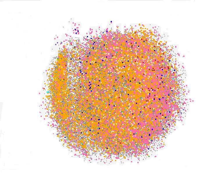
Where is AI used?

        Source: Niven Singh (https://software.intel.com)

                            2018 IEEE 68th Electronic Components and Technology Conference │ San Diego, California │ May 29 – June 1, 2018   3
Why do we care?
                                                                                                                       March, 2018

          https://www.tractica.com/newsroom/press-releases/artificial-intelligence-driven-hardware-sales-will-reach-115-billion-worldwide-by-2025/
          Reproduced by permission of Tractica

                 2018 IEEE 68th Electronic Components and Technology Conference │ San Diego, California │ May 29 – June 1, 2018                      4
Speaker Bio: Igor Arsovski

                    • Igor Arsovski is the Chief Technical Officer of the
                      GlobalFoundry’s ASIC Business Unit. He is responsible
                      for ASIC Artificial Intelligence Strategy including IP and
                      Methodology.
                    • His narrow focus is in semiconductor memories. His
                      extended focus is energy efficient building blocks for
                      Machine Learning and Automotive Electronics including
                      3D memory integration.
                    • Igor has authored 15 IEEE papers, and filed over 80 US
                      patents.

               2018 IEEE 68th Electronic Components and Technology Conference │ San Diego, California │ May 29 – June 1, 2018   5
Predictions for the future of Artificial Intelligence:
(some predict the emergence of the singularity by 2045)

                                                                                                                                 https://futurism.com/

• Most AI future predictions assume Moore’s Law continues
• More than Moore architectures and packaging are going to be key to enable AI

                    2018 IEEE 68th Electronic Components and Technology Conference │ San Diego, California │ May 29 – June 1, 2018                  6
Artificial Intelligence Devices Classification:
  Training & Inference (Automotive Example)

   Training                                                                  Inference
                              DNN
                             Training           DNN              OTA
                                                               Deployment
Data Center                                                                        Connected
                                                                                  Autonomous
   Initial DNN
  Training and
                                                                                   Computer
Continual Learning
   from Fleet                                                                          Local DNN
                                                                                    Inferencing and
                                                                                   Driving Decisions

                                        Real Time Update to Cloud

                                                                            © 2018 GLOBALFOUNDRIES   7
Artificial Intelligence Image Recognition Example

   Sum(Activations x Weights) = New Activations
                       Multiply and Add
    A[0:n]
                    W[0:n]

          • Pattern recognition requires lots of Multiplication and Accumulations (MAC)
          • Large data-sets requires large amount of Memory and MAC units
          • Value of devices measured in TOPS/s and TOPS/W
                                                                 GLOBALFOUNDRIES Confidential   8
Artificial Intelligence: Industry Trends

                                                                                           LARGE DESIGN TEAM INVESTMENT
                                                       10-50X Improvement                     NEEDED PAST GPU / FPGA
      Flexibility / Ease of Use

                                                  in TOP/s and TOP/W (CPU to GPU/FPGA)
                                                                                           100-1000X Improvement
                                                                                           in TOP/s and TOP/W (GPU to ASIC)

                                                    GPU
                                                                          FPGA                      ASICs
                                                          Performance / Power Efficiency
                                  • Quest for higher-performance / lower energy per operation
                                  • CPU to FPGA progression can be made without a chip-design team
                                  • Move to ASIC requires a fully staffed design team

                                                                                                                              9
Energy Optimization in a AI designs

            Source: MIT
                            ASIC
                                           PE         PE
                                                                                GLOBALFOUNDRIES
            DRAM            Buffer                                               Value Proposition
                           Memory
                                           PE         ALU
                                                                                 STDCELL Library
                                                                                 • Area/energy efficient
              Data Transfer Linkage             Normalized Energy Cost
                                                                                   ALU/MAC.
                                                                                 • DTCO support.
                                      PE         1x

                           RF         PE         1x                              Local Memory
                      ALU             PE           2x                            • High Speed Local SRAM
                  Buffer              PE                    6x
                                                                                 • Industry leading SRAM
                                                                                   cell density.
           DRAM                       PE                                 200x
                                Opportunity for Improvements
                                                                                                           10
Packaging Options to Meet AI Needs
Power, Performance & Cost Needs
2D Packaging Signaling speed increasing 30G to 112G
2.5D Integration 14nm HBM interface hardware verified
Stitched interposer capability for large designs
1st in volume production with 32nm
3D Integration
Lowest interface power & smallest form factor
© 2017 GLOBALFOUNDRIES 113D SRAM Memory Advantage
Memory Capacity & Energy/Access critical for AI applications
3D stacking enables multiple node memory density scaling
512
512
SRAM Memory Capacity (Mb/mm2)
3D / 8H
256
256
128
128
SRAM Memory Capacity (Mb/mm2)
64
64
32
32 3D / 4H
16
16
8
8 2D -> 3D / 4H SRAM
4 Node Gains 3D / 2H
4
2 2D -> 3D / 8H SRAM
Node Gains
12
3D / 1H
1 65 45 32 22 14 7
65 45 32 22 14 7
Process Node
Process Node (nm) (nm)
2D Memory Density 3D 1H Stack 2D Memory
3D 2HDensity
Stack 3D 4H Stack 3D 8H Stack 2DSpeaker Bio: Kailash Gopalakrishnan
Kailash Gopalakrishnan is a Distinguished Research Staff
member at IBM Research where he manages the Accelerator
Architectures and Machine Learning group at the T. J. Watson
Research Center, N.Y. Kailash has led work in the areas of
semiconductor devices, emerging memory technologies, novel
computer architectures, ASIC design and deep learning
algorithms. His current passion is centered around hardware-
software co-design of specialized architectures optimized for
deep learning acceleration by pushing the boundaries of
approximate computing techniques. He has a Ph.D. in Electrical
Engineering from Stanford University and is a member of the
IEEE.
2018 IEEE 68th Electronic Components and Technology Conference │ San Diego, California │ May 29 – June 1, 2018 13Overview
{0, 7, 1, 8, …}
• Deep Learning Training & Inference today:
• Training: Many big chips (300W) connected through proprietary links for inter-chip gradient
reduction. Racks / pods in the data center – largely accelerator-centric (> 2:1 / 4:1 over CPUs) .
• Inference: Huge push @ the edge + Standard PCIe attached < 75W cards in the data center.
• Strategic Thrusts:
• Use of Approximate Computing techniques (scaled precision tuning, compression,... ) to reduce
computation and communication for Deep Learning – training and inference.
1. Scaled Precision for Training (16/8?/4? bits) and Hyper-scaled precision for Inference (8/4/2?/1?bits).
Impact on packaging and cooling for training.
2. Use of Compression techniques to minimize bandwidth needs for Training. Impacts packaging.
• Using these techniques to define new cores for A.I. & Deep Learning SoCs.
*Primarily a further out research perspective. This brief presentation reflects my research team’s views largely – and not
those of IBM Corp broadly.
2018 IEEE 68th Electronic Components and Technology Conference │ San Diego, California │ May 29 – June 1, 2018 14Deep Learning Training : Computation vs. Communication
Deep Learning Processor Core for AI Training and Inference
(2018 Symposium on VLSI Circuits): To be presented in June 2018
AdaComp : Lossy Compression
Training with 16-bits of precision (>50X)
• Deep Learning Training is a battle between raw computational throughput (Flops),
memory bandwidth (MBW) and communication bandwidth (CBW).
• Plenty of powerful 300W accelerators with lots of Flops trying to work together on 1 large problem.
• Compute Precision improves Flops significantly – but stresses CBW and MBW.
• MBW & CBW are stressed since compute throughput grows ~ quadratically with reduction in precision.
• (Lossy) Compression techniques can dramatically improve CBW – but need to be low
overhead and should not impact algorithmic convergence.
• Will these techniques obviate the need for high bandwidth peer-to-peer connections?
2018 IEEE 68th Electronic Components and Technology Conference │ San Diego, California │ May 29 – June 1, 2018 15Peek into the Future
• DL Law of Precision Scaling expect continuous further reduction in precision.
• 8-bit Training on the horizon (end of the decade?) followed by 4-bit a few years out?
• Hyper-scaled Precision optimized DL core and system architectures – to improve computational
efficiency.
• Expect severe memory bandwidth bottlenecks (i.e. beyond 2.5D and HBM)
• Will drive the use of 3D stacking – memory (cache/scratch-pads) on top of of the processor for
compute efficiency improvements.
• Thermal challenges - given the high (>300W) power envelope
• Off-chip I/O for peer-to-peer accelerator connections is a little less predictable
• Past few generations have pushed more I/O links into the accelerator (e.g. NVLINK).
• DL Compression schemes (if > 50X) may significantly reduce bandwidth needs.
• This could simplify packaging & board design and facilitate the use of standard compliant links.
2018 IEEE 68th Electronic Components and Technology Conference │ San Diego, California │ May 29 – June 1, 2018 16Speaker Bio: Andrew Putnam
• Principal Engineer in Microsoft Azure
• Joined Microsoft Research in 2009 after Ph.D. from U. of
Washington CSE
• Co-Founder of the Microsoft Catapult project, the first to
put FPGAs in every server in the datacenter
• Bing web search acceleration
• Azure SmartNIC for Accelerated Networking
• Project BrainWave deep learning acceleration platform
• Currently leading the Azure SmartNIC FPGA team in Azure
Networking
2018 IEEE 68th Electronic Components and Technology Conference │ San Diego, California │ May 29 – June 1, 2018 17Cloud Growth is Exponential
2013 2014 2015 2016 2017
2018 IEEE 68th Electronic Components and Technology Conference │ San Diego, California │ May 29 – June 1, 2018 18Toward Specialization
~3%
~20% / year
~50%+ / year
http://preshing.com/20120208/a-look-back-at-single-threaded-cpu-performance/ Source: Bob Broderson, Berkeley Wireless group
CPU performance isn’t increasing So now we need to specialize
2018 IEEE 68th Electronic Components and Technology Conference │ San Diego, California │ May 29 – June 1, 2018 19FPGAs in the Datacenter – Project Catapult
0.5m QSFP cable from NIC to FPGA
• Bump-in-the-wire architecture NIC
• One FPGA in every server FPGA
Microsoft has deployed since 2015
Microsoft now does RTL design!
~3m QSFP cable from FPGA to TOR
2018 IEEE 68th Electronic Components and Technology Conference │ San Diego, California │ May 29 – June 1, 2018 20Project Brainwave – Deep ML on FPGA
Ethernet Switch
FPGA FPGA FPGA FPGA
CPU CPU CPU CPU
Traditional Approach Project Brainwave
2018 IEEE 68th Electronic Components and Technology Conference │ San Diego, California │ May 29 – June 1, 2018 21Deep Learning Applications
ResNet-50: 8 billion operations per image
$42
2018 IEEE 68th Electronic Components and Technology Conference │ San Diego, California │ May 29 – June 1, 2018 22Why not ASICs?
Software FPGA ASIC
2018 IEEE 68th Electronic Components and Technology Conference │ San Diego, California │ May 29 – June 1, 2018 23Speeding ASIC Integration via Chiplets
• FPGA provides common interfaces
• DDR, PCIe, Ethernet, I2C can all be FPGA
• Focus on just the core value of your ASIC
• Use FPGA logic for common software API
and “future proofing” interfaces
• Allows using separate process technology
from FPGA
• Not necessarily specific to Intel
2018 IEEE 68th Electronic Components and Technology Conference │ San Diego, California │ May 29 – June 1, 2018 24A Word of Caution – Amdahl's Law
• Deep Learning is generally only
part of the full algorithm
• Still need general-purpose CPU
platforms tightly integrated
And ruiner
of accelerator
dreams
2018 IEEE 68th Electronic Components and Technology Conference │ San Diego, California │ May 29 – June 1, 2018 25Conclusions
• Silicon customization is coming to the Cloud
• Deep Learning is pushing High-Performance Computing (HPC) from
specialized clusters into the general-purpose fleet
• Network latency is critical… but so is cost
• Advanced packaging can greatly accelerate ASIC adoption in the cloud
while still keeping pace with changes in AI/ML/Deep Learning
2018 IEEE 68th Electronic Components and Technology Conference │ San Diego, California │ May 29 – June 1, 2018 26Speaker Bio: Dan Oh
• EXPERIENCE
• Samsung Electronics, Package Development Team, Vice President
(present)
• Intel Corporation, Programmable Solution Division, SI/PI Architect (Aug.
2016)
• Rambus Inc. Technical Director (June 2012)
• EDUCATION
• Ph. D. Electrical Engineering, University of Illinois at Urbana-Champaign
• Publication
• 66 patents and patent applications
• Over 100 papers in IEEE journals and conferences
• Book “High-speed Signaling: Jitter Modeling Analysis, and Budgeting.”
2018 IEEE 68th Electronic Components and Technology Conference │ San Diego, California │ May 29 – June 1, 2018 27Package Paradigm Shift
Chip-to-chip >10㎜ ~ 1㎜ ~ 0.1㎜ ~ 0.01㎜
distance
No PCB Silicon PKG Interconnect Only Pad2Pad Bonding
DRAM
DRAM Core A SRAM Core B
HBM Logic HBM HBM Logic HBM
Logic DRAM Logic TSV
Logic
Si Interposer
Silicon -
PKG + PCB PKG on PKG RDL - Interposer 3D-SiP
Interposer
1990 2000 2010 2018 2020 SiP
• Demands for low-power & high-performance accelerate chip-to-chip integration
• Integration technology continues to drive wider interconnects
2018 IEEE 68th Electronic Components and Technology Conference │ San Diego, California │ May 29 – June 1, 2018 28Package Technology Evolution
Era of PC Era of Mobile Era of AI/HPC
Logic
CPU Memory
AP Memory TSV
2D MCM
RDL 3D SiP
(Homogeneous)
(Multi Chip Module) FOSiP Logic
Memory
F/C FBGA AP Core A SRAM Core B 3D SiP
(Heterogeneous)
FOPLP-PoP
Logic TSV
Memory
BOC Memory
W/B FBGA AP HBM Logic HBM
I-PoP
RDL Interposer
Memory HBM Logic HBM 2.5D RDL-Interposer
Ceramic W/B AP Si Interposer
PoP 2.5D Si-Interposer
2018 IEEE 68th Electronic Components and Technology Conference │ San Diego, California │ May 29 – June 1, 2018 29Logic and Memory Integration for AI
Server Edge
Application
Training Inference Inference
Throughput Throughput Throughput
Area Latency
Key Index Area Latency Area Latency
Cost Power Cost Power Cost Power
High bandwidth High bandwidth Low latency, low power
Demand High density Low latency Small form-factor
Memory HBM (4~6cube) HBM (1cube), GDDR5/6 LPDDRx, new DRAM (?)
Logic HBM
Package HBM Logic HBM
Si Interposer
HBM Logic HBM
Si Interposer
GDDR6
PKG ASIC
GDDR6
PKG
DRAM
Logic Logic 1 DRAM
RDL
Si-interposer CoW RDL interposer Si-interposer CoS SiP Module Advanced SiP Fan-out PKG
2018 IEEE 68th Electronic Components and Technology Conference │ San Diego, California │ May 29 – June 1, 2018 30GDDR6 vs HBM
GDDR6 can be a good replacement of HBM for
server inference, HPC, block chain, and automotive applications
Memory bandwidth assumption: 128GB/s : GDDR6
HBM(Aquabolt, 4H): 1cube : HBM(Aquabolt)
GDDR6: 2ea
Bandwidth Density Power Cost
1-cube(300GB/s) 20%↑ 8.xxW 3.7X 73%↓
x1024 4GB = 4GB
6.xxW
2 PKGs
128GB/s 1X
x128
HBM2.4 GDDR6 HBM2.4 GDDR6 HBM2.4 GDDR6 HBM2.4 GDDR6
(1cube, 4H) (2 PKGs) (1cube, 4H) (2 PKGs) (1cube) (2 PKGs) (1cube) (2 PKGs)
2018 IEEE 68th Electronic Components and Technology Conference │ San Diego, California │ May 29 – June 1, 2018 31Potential Memory Architectures
3D memory integration addresses
Power, Throughput, Latency and area except Cost
Mobile AI Server Inference Server Training
DRAM SRAM Stack
Memory Core
Logic
Substrate
Logic
Substrate Inference
High Bandwidth Memory
(Non-HBM, x128~256) SRAM Stacking
Process-In-Memory (PIM)
DRAM SRAM HBM-base
Mono die 2~4 stacked dies 2~8 stacked die
Bandwidth: 1x Bandwidth: 2x ~ 4x Bandwidth: 2x ~ 16x
2018 IEEE 68th Electronic Components and Technology Conference │ San Diego, California │ May 29 – June 1, 2018 32Future 3D System Integration Schemes
Heterogeneous Homogeneous
Integration Integration
Core A SRAM Core B CoW
CoW Wafer stack W2W CoW
Logic
Logic Logic
CoW
W2W CoW
Core A SRAM Core B
D2W
Logic D2W
D2W W2W
Logic
W2W
: High Throughput
D2W
: High Yield
High-end System Integration D2W + W2W CoW & High Throughput
(different node, different die, PMIC, etc) New memory
Die partitioning Same die multi-stack
2018 IEEE 68th Electronic Components and Technology Conference │ San Diego, California │ May 29 – June 1, 2018 33Conclusions
• Package integration continues to drive new computing
architectures
• From 1D to current 2.5D, and moving onto 3D…
• Silicon interposer and HBM serve current AI training needs
• 3D integration serves further training requirements
• Inference may require new memory solutions
• Small high bandwidth memory or
• Low latency SRAM devices
2018 IEEE 68th Electronic Components and Technology Conference │ San Diego, California │ May 29 – June 1, 2018 34Speaker Bio: Madhavan Swaminathan
Professor Madhavan Swaminathan is the John Pippin Chair in
Microsystems Packaging and Electromagnetics in the School of
Electrical and Computer Engineering and Director, Center for Co-
Design of Chip, Package, System (C3PS), Georgia Tech. He is the author
of 450+ refereed technical publications, holds 30 patents, primary
author and co-editor of 3 books, founder and co-founder of two start-
up companies and founder of the IEEE Conference Electrical Design of
Advanced Packaging and Systems (EDAPS) sponsored by EPS.
2018 IEEE 68th Electronic Components and Technology Conference │ San Diego, California │ May 29 – June 1, 2018 35Limits of Modern EDA
• The need for design “re-spins” has not been eliminated
• Many of the observed failures during qualification testing are the direct result of
an insufficient modeling capability
– Sources of such failures include mistuned analog circuits, signal timing
errors, reliability problems, and crosstalk [*]
• Simulation-based design optimization has had only limited success
– Simulation “in-the-design-loop” often too slow and leads to impractical
designs
[*] Harry Foster, “2012 Wilson Research Group Functional Verification Study,”
http://www.mentor.com/products/fv/multimedia/the-2012-wilson-research-group-functional-
verification-studyview
2018 IEEE 68th Electronic Components and Technology Conference │ San Diego, California │ May 29 – June 1, 2018 36Model-Based Design Paradigm
• Fast-to-evaluate “learned” model replaces detailed slow model in
design, and design optimization/feasibility problems
2018 IEEE 68th Electronic Components and Technology Conference │ San Diego, California │ May 29 – June 1, 2018 37Optimization using ML
H.M.Torun, M.Swaminathan et al,
TVLSI, 2018
Main objective is to use ML based optimization to automate the design cycle and minimize human
intervention on optimization and tuning of control parameters of integrated systems.
Active Learning:
uses zero training data.
ensures convergence to global optima while minimizing the required CPU time.
capability of handling very large number of parameters (50+).Integrated Voltage Regulator Optimization
Overall IVR Architecture Embedded Solenoidal Inductor
Hand Tuned Non-Linear GP-UCB IMGPO TSBO
Inductor 11.3 mm2 25.19 mm2 5.18 mm2 6.64 mm2
5.16 mm2
Area (+56.1%) (+79.6%) (%0.4) (%28.1)
Peak
79.4% 78.6% 84.9% 84.4% 85.1%
Efficiency
>185 min 117.33 min 115.6 min
CPU Time N/A 50.1 min
(+72.9%) (+57.4 %) (+56.7 %)
Integrated Voltage Regulators are used to increase efficiency and conserve power in microprocessors (Ex: Intel Gen
Embedded Solenoidal Inductor
4)
Objective is to maximize IVR efficiency while minimizing inductor area
IVR efficiency is affected by inductor and buck converter.
Assuming LDO, PDN and LOAD is fixed.
Solenoidal Inductors with magnetic cores are used
Multiple trade-offs: ESR, DC resistance, inductance, lateral area
Tune inductor control parameters to maximize efficiency (8 – 10 dimensions)
Hand Tuned: S. Mueller et al., ECTC’16.
Optimized:H. M. Torun et al., TVLSI ‘18Design Space Exploration (using Transfer Learning)
Predictive Predictive Predictive Predictive
Model #2 Model #2 Model #2 Model #2
Lots of Data for Lots of Data for Transfer Very Scarce
Lots of Data for Data for Design
Design Option #1 Design Option #2 Design Option #1 Learning
Option #2
Input Input Input Input
Parameters #1 Parameters #2 Parameters #1 Parameters #2
Conventional Method Proposed Method
(Different Model for Different Designs) (Re-use previous model to derive new model)
Design space exploration involves developing models for many different topologies.
• Ex: Sigle-ended vs differential signaling, shielded vs unshielded signal lines etc.
Different topologies can share information that can be exploited using transfer learning to significantly
reduce CPU time and effort to derive new models.Model transfer from Microstrip to Stripline
The goal is derive a model to predict
frequency dependent RLGC parameters
for both microstrip and stripline
structures.
Model for microstrip line has already
been developed and validated to have
high accuracy (assumption – prior data)
The model for microstrip is then re-used
using transfer learning to derive a new
model for stripline.
Preliminary results show transfer
learning approach significantly reduces
CPU time to derive the model for
stripline compared to different models
for each structure.Design Space Exploration using ML
High-Dimensional Data Mapping to Low Dimensional Space
Inference
Optimization
Hardware Security
Sensitivity
Yield
ManufacturabilityAnd to you Skeptics….
Machine Learning can help
Eliminate the frustrations of Design and Simulation by AUGMENTING the engineer but never
REPLACING the engineer. Engineers are the thinkers! Computers are the doers! Machine
Learning is the enabler!Q&A 2018 IEEE 68th Electronic Components and Technology Conference │ San Diego, California │ May 29 – June 1, 2018 44
You can also read