Analysis and improvement of the "red/blue spot" of TFT-LCD - E3S Web of Conferences
←
→
Page content transcription
If your browser does not render page correctly, please read the page content below
E3S Web of Conferences 300, 01017 (2021)                                 https://doi.org/10.1051/e3sconf/202130001017
ICEPESE2021

       Analysis and improvement of the "red/blue spot"
       of TFT-LCD
       Yuanyuan Li1,2, Xu Zhang1,2, Jianming Wang1, Huasheng Yan2, and Zaijun Cheng1,*
       1Schoolof Opto-electronic and Communication Engineering, Xiamen University of Technology,
       Xiamen 361024, China
       2Consumer Quality Department of Tianma Microelectronics Co., Ltd, Fujian Xiamen 361000, China

                     Abstract. "Red/blue spot" is a common undesirable phenomenon in small
                     and medium-sized TFT-LCD products, which directly affects the display
                     quality of the product. It has always been a difficult problem in the display
                     industry, which greatly reduces the market competitiveness of
                     corresponding products. In this work, pressure tests are carried out on
                     liquid crystal panels with different sizes and resolutions. The effects of
                     different factors such as the flatness of the photo space, the distribution
                     density of the spacers, and the glass thickness on the "red/blue spot" are
                     compared. By increasing the flatness of the PS station, the septum
                     distribution density, and the thickness of the glass, the sample's
                     anti-extrusion ability can be increased by 46.1%, 30%, and 23.1%,
                     respectively. The experimental results can provide the basis for industry to
                     further improve quality of products.

       1 Introduction
           With the rapid development of science and technology, thin film transistor liquid crystal
       display (TFT-LCD) has gradually replaced traditional displays with its many advantages
       such as low power consumption, high image quality and light weight[1-2]. Various LCD
       panel companies focus on improving the display quality of their products[3]. Among them,
       "red/blue spots", as one of the many common poor picture quality in the display industry,
       has received extensive attention from researchers.
           In the manufacturing process of the LCD panel, in order to ensure the uniformity and
       stability of the cell thickness of the liquid crystal cell, the photo spacer (PS) between the
       color film (CF) substrate and the TFT array substrate plays an irreplaceable role[4-5]. The
       PS prepared in the liquid crystal display can better control the uniformity of the cell
       thickness to prevent related display defects.
           The main reason for the occurrence of "red/blue spots" is that when the LCD panel is
       subjected to an unbearable external force, the PS in the box scratch the alignment film and
       cause light leakage. The influencing factors include the design of the flatness of the PS
       station, the distribution of main/supplement (M/S) PS, and the glass thickness. This work
       compares the pressure test results of different LCD panels, explores the influence of
       different factors on the "red/blue spots", and proposes a solution to the "red/blue spots".

       *   Corresponding author: 2011111002@xmut.edu.cn

© The Authors, published by EDP Sciences. This is an open access article distributed under the terms of the Creative Commons
Attribution License 4.0 (http://creativecommons.org/licenses/by/4.0/).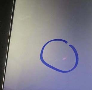
E3S Web of Conferences 300, 01017 (2021) https://doi.org/10.1051/e3sconf/202130001017
ICEPESE2021
2 Stress test methods and the mechanism of "red/blue spots"
2.1 Stress test method
The experiment test uses a universal tester (Shimadzu, AG-X plus5kN/1kN,
1N~4800N/980N). The outer packaging of the sample should be removed before test, and
the tester will inspect the appearance and electro-display effect of the sample.
Installation of indenter and jig: Choose a rubber indenter with a pressure rod Φ 10 mm
and an indenter Φ 15 mm ball head. The fixture platform requires a flat stage with a hollow
center and a diameter of 30 mm. As shown in Fig. 1(a), the pressure gauge is vertically and
positively pressed against the center of the liquid crystal panel.
(a) (b)
Fig. 1. (a) PS fixture test point; (b) Sample fixing method.
Sample fixation: As shown in Fig. 1(b), the sample is placed on the stage with the CF
side facing up and the indenter to the center of the sample.
Test conditions: The descending speed of the pressure rod is 5 mm/min, the force value
starts from 0.5 kgf, and the dwell time is 5s each time. After each test, remove the sample
from the fixture and check if there is any "red/blue spot". If yes, record the force value as
the critical force value of the sample; if not, increase by 0.1kgf until it appears.
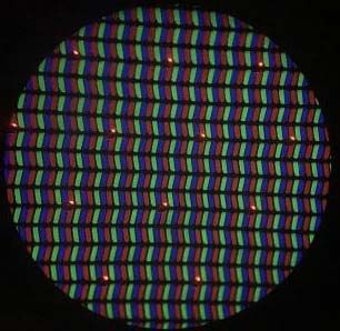
2.2 "Red/Blue Spots" Phenomenon
The picture in Fig. 2(a) shows the macroscopic phenomenon of red spot, and (b) shows the
microscopic phenomenon of it. Put the squeezed sample on the fixture that has been lit, and
red spots can be observed when the screen is switched to the dark state. Under the
microscope it can be seen that small colored bright spots are close to the black matrix.
(a) (b)
Fig. 2. (a) Macro picture of Red spot; (b) Micro picture of Red spot.
2.3 Analysis of the mechanism of "red/blue spots"
Photo spacers are used in the manufacture of liquid crystal panels to largely control the cell
thickness of the liquid crystal panel and to further control the display quality of the liquid
crystal panel[6-7]. When the liquid crystal panel is subjected to an external force, the spacer
2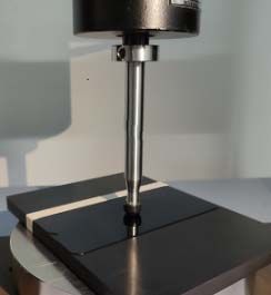
E3S Web of Conferences 300, 01017 (2021)                            https://doi.org/10.1051/e3sconf/202130001017
ICEPESE2021

      is compressed, and if the external force is removed within its elastic recovery limit, it will
      return to its original state. If the external force exceeds the elastic recovery limit, the PS
      will scratch the alignment film in the light-transmitting area on the TFT array substrate, and
      then lose the liquid crystal alignment ability[8-9]. Due to people's demand for
      high-resolution products, the width of the black matrix will be designed to be smaller as
      required, so the position of the scratched alignment film cannot be blocked, and colored
      spots will be observed under the black screen[10].
          In order to ensure a better display effect of the LCD screen, the PS will be designed on
      the blue and red pixel units after comprehensive consideration of the test. If the PS position
      of the red pixel unit scratches the alignment film, it will appear red spots, and if the
      alignment film at the PS position of the blue pixel unit is scratched, blue spots will appear.

      3 Experimental results and discussion
      The above-mentioned stress tests were carried out for liquid crystal panels of different
      designs, and the influence of PS station flatness design, PS distribution density and glass
      thickness design on the adverse effects of "red/blue spots" on the sample were analyzed.
      Fig. 3 is a schematic diagram of the stress test experiment.

      Fig. 3. Schematic diagram of PS extrusion test.

      3.1 The impact of PS station position flatness (PLN) on "red/blue spots"
      Fig. 4 shows the SEM images of the flatness of the PS station position of different schemes.
      From top to bottom, the PS station flatness of plan A is the best, the PS flatness design of
      plan B is second, and the PS design of plan C has no flatness. Since the PS station positions
      of the three schemes are the same, the schematic diagram of the PS station position is
      marked in scheme B in the figure.
                                                        Table 1. PS anti-extrusion force during flatness
                                                                design of different PS stations.

                                                                                            PS Fight
                                                        condition    flatness   angle
                                                                                            pressure

                                                         Plan A        10.8     50.37        1.4kgf

                                                         Plan B        9.8      43.17        1.1kgf

       Fig. 4. SEM images of the flatness design         Plan C        8.6      39.51        0.8kgf
       of different PS stations.
          Experimental test the size of the anti-extrusion force of different PS station flatness, and
      the experimental results are shown in Table 1. The flatness design of plan A is 10.8, and the
      PS anti-extrusion force measured by the experiment is 1.4 kgf. The plan C is designed
      without any flatness, and the experimental PS anti-extrusion force is 0.8 kgf, which shows

                                                        3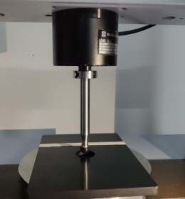
E3S Web of Conferences 300, 01017 (2021)                          https://doi.org/10.1051/e3sconf/202130001017
ICEPESE2021

      that the flattening of PLN can make PS anti-extrusion force increased by 46.1%.

      3.2 The influence of PS distribution density on "red/blue spots"
      As shown in Table 2, this work uses experiments to verify the relationship between the
      different M/S PS distribution densities (um2/mm2) of different products and the maximum
      force that the product can withstand without red/blue spots. It can be seen from Table 2 that
      as the support density of the septum increases, the PS compression resistance increases by
      30%. This shows that when the PS density is increased, the probability of "red/blue spots"
      will decrease under the same pressure value.
            Table 2. The experimental values of    PS density and compression force of each sample.
                   sample name          (M/S)PS density(%)            PS Fight pressure(kgf)
                       A1                   0.083/2.56                         1.3
                       A2                   0.085/2.62                         1.4
                       A3                   0.088/2.66                         1.5
                       A4                   0.09/2.94                          1.5
                       A5                   0.082/3.05                         1.6
                       A6                  0.083/3.506                         1.6
          Increasing the PS density can effectively improve the "red/blue spots", but with the
      increase PS, the probability of the appearance of low-temperature bubbles also
      increases[11]. Under the action of external force, the excessive density of the PS will make
      the fluidity of the liquid crystal worse, resulting in the phenomenon of vacuum bubbles.

      3.3 The influence of glass thickness on "red/blue spots"

      Fig. 5. The maximum pressure value of the "red/blue spots" non-appear in different glass thicknesses.
      In order to meet the current market demand for smart wearable products, small-size LCD
      panels need to be thinner and lighter without affecting the display. At present, the thinning
      of TFT-LCD mainly uses thinning technology (Slimming)[12], and major panel
      manufacturers can reduce the thickness of the box to 0.15 mm or 0.20 mm. As shown in Fig.
      5, the squeezing force value with the glass thickness of 0.15 mm and 0.2 mm is 1kgf and
      1.3 kgf, respectively. The PS squeezing force value has increased by 23.1%, indicating that
      as the glass thickness increases , PS anti-extrusion ability is improved.

      4 Plan to improve "red/blue spots"
      According to the above experiments and analysis, it is known that the effective method to

                                                       4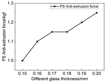
E3S Web of Conferences 300, 01017 (2021)                      https://doi.org/10.1051/e3sconf/202130001017
ICEPESE2021

      improve the red/blue spots is to increase the flatness design of the PS station, the PS
      distribution density, and the thickness of the glass. When the box is vacuumed, it is
      necessary to consider the offset of the box, the size of the PS and the position accuracy of
      the PS. The flatter the PLN, the greater the compression resistance of PS. On black screen,
      the probability of "red/blue spots" appearing is smaller. For TFT-LCD products with high
      resolution and high transmittance, it is necessary to reasonably increase the density of
      spacers on the color film substrate without reducing the aperture ratio and low-temperature
      bubbles. The current demand for lightness and thinness of small-sized products requires an
      appropriate increase in the thickness of the glass on the basis of relatively lightness and
      thinness, so as to resist the destructive force of external forces on the liquid crystal panel.

      5 Conclusion
      In conclusion, when the LCD panel is subjected to an irresistible pressure, the PS scratch
      the alignment film on the TFT array substrate, making it impossible to align the liquid
      crystal normally. Therefore, the phenomenon of "red/blue spots" can be observed under a
      black screen, while under a microscope it is a colored bright spot. According to the
      experimental results, with improving the flatness of the PS station, increasing the spacer
      distribution density and the thickness of the glass, the anti-extrusion ability of the sample
      can be increased by 46.1%, 30% and 23.1%, respectively. This work expounds the
      influencing factors of the "red/blue spot" phenomenon of the LCD panel under the action of
      pressure and proposes improvement plans to provide help for the improvement of the
      products’ quality.

      Acknowledgments
      This research was supported by Natural Science Youth Innovation Fundation of Xiamen
      City (Grant No.3502Z20206077), the Scientific Research Climbing Project Foundation of
      Xiamen University of Technology (Grant No.XPDKT20011) and Postgraduate Science and
      Technology Innovation Project Fund of Xiamen University of Technology (Grant Nos.
      YKJCX2019062 and YKJCX2019071).

      References
      1.    Q G.Ma.Electronic Industry Press.90-92,418-419(2011)
      2.    ZH Y.SHEN, CH Y.Dong.Publishing House of Electronics Industry. 222-227(2012)
      3.    Y.AI,L P.LIU,J D.ZHOU. Liquid crystal and display.02(2015)
      4.    H ZHOU.Shanghai Jiaotong University.(2014)
      5.    S. LU, J G.LU,J.ZHU. Shanghai Jiaotong University.04(2015)
      6.    C Q. CHEN .South China University of Technology.(2017)
      7.    X J.LI ,Y L.ZHAO ,P.LI.LCD and display.07(2017)
      8.    Y CH.WANG ,ZH.LI ,R.LI .Modern Display, 20(06): 25-28(2009)
      9.    W CH. CHEN ,Q.LING ,Q.JIANG .Electronic world.16(2019)
      10.   ZH.CHEN ,H.LI ,X.CHEN.Application of Electronic Technology.37(06): 123-126(2011)
      11.   SH.CHENG ,T.WANG ,M.ZHANG.LCD and display.05(2011)
      12.   Y G.FAN ,J P.LI ,S X.SONG.2014 China Flat Panel Display Conference. (2014)

                                                    5
You can also read