Autonomous on-Chip Debugging for Sensors Based on AVR Microcontrollers
←
→
Page content transcription
If your browser does not render page correctly, please read the page content below
Journal of Sensor Technology, 2021, 11, 19-38
                                                                                                   https://www.scirp.org/journal/jst
                                                                                                            ISSN Online: 2161-1238
                                                                                                              ISSN Print: 2161-122X

Autonomous on-Chip Debugging for Sensors
Based on AVR Microcontrollers

Antoine Bossard

Graduate School of Science, Kanagawa University, Kanagawa, Japan

How to cite this paper: Bossard, A. (2021)      Abstract
Autonomous on-Chip Debugging for Sen-
sors Based on AVR Microcontrollers. Jour-       Sensors are often based on minimalistic microcontrollers for their reduced
nal of Sensor Technology, 11, 19-38.            power consumption and size. Because of the specific hardware of sensors,
https://doi.org/10.4236/jst.2021.112002
                                                their software development, including debugging, is also particular. Simula-
Received: May 3, 2021
                                                tors and external computers are conventional approaches to sensor debug-
Accepted: June 18, 2021                         ging, but they both face limitations such as the supported hardware and de-
Published: June 21, 2021                        bugging conditions. In this paper, we propose a fully autonomous on-chip
                                                debugging solution for sensors (and other devices) based on AVR microcon-
Copyright © 2021 by author(s) and
Scientific Research Publishing Inc.
                                                trollers, with a particular focus on human-machine interaction. The proposal
This work is licensed under the Creative        is then validated in practice through various experiments, notably involving
Commons Attribution International               real-world sensors. Formal measurement of the induced overhead is also
License (CC BY 4.0).
                                                conducted, which eventually demonstrates the applicability of the proposal.
http://creativecommons.org/licenses/by/4.0/
               Open Access
                                                Keywords
                                                RISC, Computer, Architecture, ISA, Software, Assembly, Electronics, Green
                                                Computing, HMI

                                              1. Introduction
                                              Comparable to some embedded systems, sensors need to be efficient with re-
                                              spect to their power consumption, especially when used in a mobile environ-
                                              ment or the Internet of things (IoT), and this is directly related to the space re-
                                              quired by the sensor hardware [1]. As a result, such devices are often based on
                                              particular chips that can help satisfying these requirements. The microcontrol-
                                              lers that implement the AVR or ARM processor architectures are examples of
                                              such chips [2] [3]. The Arduino Uno and BBC Micro Bit devices are concrete
                                              examples of devices based on such microcontrollers, whereas a device such as
                                              the Raspberry Pi features a more powerful processor—it is the system on a chip
                                              (SoC) approach [4] [5] [6].

DOI: 10.4236/jst.2021.112002       Jun. 21, 2021                   19                                 Journal of Sensor Technology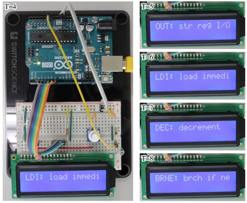
A. Bossard

                                  Besides, as such devices, sensors, often rely on specific hardware components
                               notably to implement their sensing features [7], their software development is
                               very specialised in the sense that the microcontroller program needs to interact
                               with the hardware components, with each having its own specificities like I/O
                               control and analog-to-digital conversion. Furthermore, because we rely here on
                               low-level programming, there is a notable lack of interfacing standardization across
                               those peripherals, something which is commonly realised by the architecture
                               layers of the operating system in the case of more advanced computer systems.
                               The large number of available libraries for sensors used with an Arduino board
                               is a good indicator of this situation. And obviously, a debugging solution that is
                               able to adapt itself to such a specialised software development is required as well
                               [8].
                                  We propose in this paper a fully autonomous on-chip debugging (OCD) solu-
                               tion for sensors and other devices that are based on AVR microcontrollers. This
                               approach particularly enhances human-machine interaction for the debugging
                               of sensors. In simple terms, its principle is as follows: a liquid crystal display
                               (LCD) panel is connected to the board with a minimally invasive method and
                               each microcontroller (processor) instruction of the original program (i.e. of the
                               program being debugged) that is about to be executed is displayed in real-time
                               on the LCD, just before its execution. This is a rather natural approach but its
                               realisation is highly challenging in several aspects as detailed hereinafter. For in-
                               stance, a debugging solution like the one proposed in this paper cannot be rea-
                               lised by simply reading (parsing) assembly instructions from the machine code
                               for the microcontroller and then using a conventional program, say, written in
                               the C language to print them on the display. The objective of this research is to
                               show on the display real-time information about the processor instruction that is
                               about to be executed, and this cannot be achieved with a conventional approach
                               based, say, on a program written in C, and the classic toolchain (e.g. the devel-
                               opment framework that corresponds to the selected hardware). The merit of the
                               proposal compared to the conventional approaches is further discussed in Sec-
                               tion 2.
                                  This work started from the following fact: as computers are increasingly com-
                               plex devices, one of the most recurrent HMI issues is when the system fails to
                               respond. This is usually a frustrating situation as the state of the machine re-
                               mains unknown to the user. Aiming at investigating further this issue and possi-
                               ble solutions, we have selected a simple device, a microcontroller, and some of
                               its applications, sensors, and we describe hereinafter our approach which fully
                               resolves this HMI issue: at any time, the state of the device is known. The moti-
                               vation and contribution of our proposal with respect to the sensor HMI issue is
                               further explained in the next section.
                                  The rest of this paper is organised as follows. Previous and related works are
                               discussed in Section 2, notably to emphasise the contribution of the proposal.
                               Then, preliminaries for the proposal are detailed in Section 3. Next, the proposed
                               debugging system is detailed in Section 4. It is then validated in practice in Sec-

DOI: 10.4236/jst.2021.112002                         20                                 Journal of Sensor Technology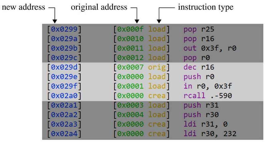
A. Bossard

                               tion 5 and formally evaluated in Section 6. The obtained results are subsequently
                               discussed in Section 7. Finally, this paper is concluded in Section 8.

                               2. State-of-the-Art and Contribution
                               Regarding previous and related works, simulators are one conventional ap-
                               proach to debugging for such microcontrollers. They are numerous and availa-
                               ble on various operating systems; Paulware Arduino Debugger [9] and UnoAr-
                               duSim [10] are two examples of such works. Unlike those, the research described
                               and evaluated in this paper realises “live”, in situ debugging, that is directly on
                               the chip, with thus the great advantage of being able to handle any program that
                               uses any kind of sensor, and hardware in general, which a conventional simula-
                               tor would not support and would hence not be able to debug such a program
                               properly. Concretely, simulators usually give a list of the supported libraries: for
                               instance, UnoArduSim only supports the TFT, SD, Stepper, Servo, SoftwareSeri-
                               al, Wire, SPI, and EEPROM libraries out of the official, standard thirteen libra-
                               ries [11].
                                  More closely related to our work, some approaches such as those of [12] and
                               [13] collect debugging information directly from the microcontroller but then
                               need additional processing by an external computer. Compared to our proposal,
                               those approaches are not autonomous, and they suffer from a very high cost:
                               those methods are in fact very demanding with respect to the required additional
                               hardware and the necessary software environment needed to process the col-
                               lected debugging information. Besides, these works are yet another proof of the
                               relevance of on-chip debugging. The development environment provided by the
                               microcontroller manufacturer, Microchip Studio for AVR and SAM devices
                               (formerly Atmel Studio) and notably its debugger component [14] (see also
                               [15]), and the portable debugger GNU Debugger (GDB) [16] are other examples
                               of debugging solutions that follow this conventional approach, and with its li-
                               mitations.
                                  In addition, from the system security point of view, it is worth noting that our
                               proposal relies neither on a JTAG interface as [17] and the previously cited works
                               [12] and [13] nor on permanent debugging (and diagnosis) code, two exploita-
                               tion vectors pointed out for instance in [18]. This security issue induced by the
                               JTAG interface is also mentioned in the work described in [19] (and in [20]),
                               work which however still has a very high cost for the reasons given in the pre-
                               vious paragraph. A similar debugging approach, and with thus the same limita-
                               tions, is provided by some ATmega microcontrollers with the debugWIRE sys-
                               tem [21] [22]. Furthermore, unlike such an approach, and although some minor
                               adjustments might be needed, our approach is applicable to any microcontroller
                               based on the AVR instruction set architecture. In fact, the proposed debugging
                               system is universal in that it is applicable to any AVR program, no matter how it
                               has been produced (compiled from C, assembled, etc.).
                                  We next further explain the motivation and contribution of our proposal with
                               respect to the HMI issue. The time (duration) and place of the debugging process

DOI: 10.4236/jst.2021.112002                        21                                 Journal of Sensor Technology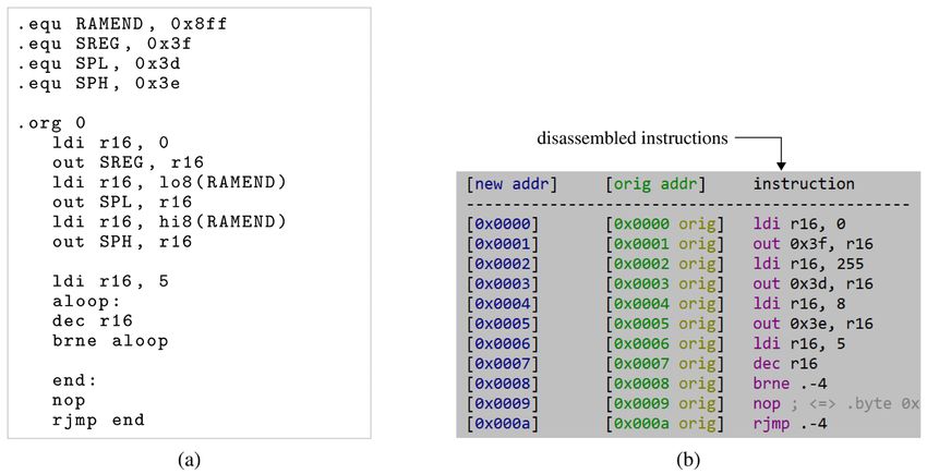
A. Bossard

                               is another reason for the high cost mentioned for the conventional approach
                               based on an external, supplemental device specially used for debugging. The es-
                               sence of the proposed system is about being “in situ”, which means of course on-
                               chip debugging, but also that the sensor should be debugged and monitored in
                               real conditions. Here, time and place are two essential such conditions which re-
                               late to on-site deployment and on-site testing of the sensor device.
                                   Time, for the duration of the debugging and monitoring process: the sensor
                               system should be in use for a long time enough, and needs to be easily and regu-
                               larly checked (e.g. [23]). This is not possible with an external computer used for
                               debugging: even if that supplemental computer can be used for debugging au-
                               tomatically for a long time, its monitoring can only be done regularly on a re-
                               stricted time interval as the programmer can only stay a limited time in front of
                               it. With the proposed system, since it implements a fully autonomous debugging
                               solution, the sensor device can stay at all times near the programmer, like at home,
                               for monitoring on wide time intervals.
                                   And the place (location) of the sensor device is even more critical: it needs to
                               be used in its real environment otherwise it makes little sense to do the sensing
                               (e.g. air quality monitoring [24]). This is again not possible with an external
                               computer used for debugging; the reader can simply imagine designing a sensor
                               device for transportation systems (thus aimed at a mobile environment), domes-
                               tic usage, and so on: the external computer for debugging cannot reasonably be
                               carried and placed nearby the sensor device in real conditions.

                               3. Preliminaries
                               A schematic of a sample circuit is given in Figure 1; the one used in this research
                               is based on an Arduino Uno Rev3, which is itself based on a 28 PDIP ATme-
                               ga328P microcontroller, coupled with an HD44780U-compatible LCD panel op-
                               erating at 5 V. The pins that correspond to the three ports B, C, D of the micro-
                               controller are emphasised. This is a rather conventional usage of an HD44780U-
                               compatible LCD panel in the 4-bit operation mode (i.e. using four data bus pins:

                               Figure 1. Schematic of a sample circuit: the one used in this research is based on an Ar-
                               duino Uno Rev3, which is itself based on a 28 PDIP ATmega328P microcontroller.

DOI: 10.4236/jst.2021.112002                          22                                  Journal of Sensor Technology
A. Bossard
DB4 to DB7), yet it can be noted that all connections are smartly gathered at one
single port (D) in order to minimise the number of pins reserved for debugging.
Six pins of the microcontroller are thus allocated to (i.e. reserved for) the de-
bugger, which is optimally low considering the hardware involved. We on pur-
pose leave the two pins 0 and 1 of port D available as they are used for the board’s
serial communication (RX and TX, respectively), a communication feature which,
although not used by the proposed debugging system, may well be used by the
program to be debugged. Since no data is read from the LCD panel, only written
to it, the R/W pin of the LCD panel is directly wired to the earth (i.e. R/W to 0 so
as to set the LCD panel in write mode). An overview of the actual prototype is
given in Figure 8.
4. On-Chip Debugging
The principle of the proposed on-chip debugging system for sensors based on
AVR microcontrollers is illustrated with a flow chart in Figure 2: the proposed
system consists of two main components, the disassembler and the injector, which
are detailed hereinafter. The dashed lines on the right side of the diagram indi-
cate abbreviation of the input and output objects for the sake of readability. A
HEX file contains ASCII byte code as per the Intel HEX standard [25]. The HEX
file of the original program thus represents the machine code of the program
that will be subject to debugging. The final HEX file is eventually uploaded into
the microcontroller to be run (to this end, we rely on the default bootloader and
avrdude (version 6.3)).
For reference, we also give in Figure 3 a simplified UML class diagram of the
proposed system as it provides relevant information to facilitate the under-
standing of the system description given in the rest of this section. Most notably,
this class diagram shows the non-trivial relations which involve the main Disas-
sembly class. An object of this class can in fact either be instantiated from one
Hexbytes object (representing one HEX file)—this is the disassembler use case,
or from three Disassembly objects—this is the injector use case.
Figure 2. Flow chart illustrating the principle of the proposed debugging system. (The
dashed lines on the right side of the diagram indicate abbreviation of the input and out-
put objects.)
DOI: 10.4236/jst.2021.112002 23 Journal of Sensor TechnologyA. Bossard
Figure 3. Simplified UML class diagram of the proposed debugging system. It notably shows
the non-trivial relations that involve the main Disassembly class.
The other software tools used in this research are based on the GNU Binutils
(version 2.26): the assembler is avr-as, which is part of the GNU as assembler
collection; the linker is avr-ld, from GNU ld; the translator is avr-objcopy, from
GNU objcopy. As briefly explained previously, the HEX file of the original pro-
gram can have been produced by various means: compiled from C with avr-gcc,
assembled from ASM with avr-as, and so on.
4.1. The Disassembler Component
It is recalled that reverse engineering of machine code for such microcontrollers
is limited to assembly code. Assembly code in fact maintains a 1-to-1 corres-
pondence to the machine code (thus comparable to a bijective function in ma-
thematics), or almost (e.g. there are instruction “synonyms”). However, it is not
possible to reverse machine code back to, for instance, the original code written
with the C language since compilation of C code to machine code loses informa-
tion: there is no 1-to-1 mapping between C code and machine code.
Although, as presented in Section 2, there exist several disassemblers for AVR
programs [14] [15] [16] [26] [27] [28], as this research project requires very
low-level manipulation of machine code instructions and their addresses (espe-
cially for the injector component of the proposed system that is detailed in the
next section), we have based the disassembler component of the proposal on our
own AVR disassembler.
First, the HEX file of the original program (i.e. the program that is to be de-
bugged) is parsed by reading Intel HEX records [25]: from this process is ob-
tained an address-byte table (a map; if needed, the bytes are reordered according
DOI: 10.4236/jst.2021.112002 24 Journal of Sensor TechnologyA. Bossard
to their addresses, although usually the byte order matches the addresses declared
in the HEX file). Here, the addresses are byte-based.
Second, the entries of this address-byte table are iterated two-by-two in order:
two consecutive bytes are merged since an AVR instructions on 8-bit AVR de-
vices consists of one or two words [29]. Bits of the first word (i.e. the first two
bytes) are thus used to identify the instruction’s opcode and operands. The next
word is read when the identified instruction is double-word, typically instruc-
tions that involve a full, 16-bit memory address such as CALL. During this process,
the word-based address of the instruction is calculated and its operands, if any,
are retrieved. As a result, an address-instruction table (map) is obtained; this ta-
ble is a perfect match of the instructions, and thus another representation, of the
original program.
The source of a sample original program—then assembled—and the corres-
ponding address-instruction table that is output by the disassembler component
are shown in Figure 4(a) and Figure 4(b), respectively. In the latter figure, there
are two address columns: the leftmost one is for the new, possibly recalculated
instruction address, and the second one shows the original address of the in-
struction. Since we illustrate in this section the disassembler component on its
own, the two addresses are equal for each table entry (i.e. instruction). This sample
source code shows typical microcontroller initialisation instructions and a loop
example: it can be noticed that the relative jump offset of the branching instruc-
tion BRNE is automatically calculated by the assembler, which stores it in words;
the disassembler then restores it in bytes and prints it in accordance with the as-
sembler (avr-as) syntax.
Finally, it should be noted that, as illustrated in Figure 2, not only is the dis-
assembler component applied to the machine code of the original program, but
it is also applied to the machine code of the debugger that will be further processed
by the injector component as detailed next.
Figure 4. (a) The source code of a sample original program—then assembled—and (b)
the corresponding address-instruction table that is output by the disassembler compo-
nent of the proposed debugging system.
DOI: 10.4236/jst.2021.112002 25 Journal of Sensor TechnologyA. Bossard
4.2. The Injector Component
The second major part of the proposal is the injector component, whose purpose
is to carefully intermingle the original program instructions with new instruc-
tions for debugging. To this end, the recalculation of the addresses used by the
original program instructions, for instance destination addresses for absolute
calls, jumps and offsets for relative ones, is a tedious yet critical task—a program
for, say, sensor control, can hardly be considered without such calls and jumps
as they make the logic of the program.
As shown in Figure 2, the injector component takes as input the instructions
of the original program, together with their (original) addresses, as well as the
instructions of the debugger code. It produces a new assembly source file that is
to be assembled as usual (avr-as), then linked and converted to machine code in
the Intel HEX format. Then, it is uploaded to the microcontroller board for ex-
ecution in what we can call debugging mode. More precisely, the injector’s input
is split into the initialisation code of the debugger, which makes the first part of
the output assembly file, thus comparable to a prefix to the program being de-
bugged, and the code of the debugger (called the step code) that is to be injected
at each instruction of the original program.
The injection process is done in two passes: the first one is to inject instruc-
tions and calculate their new addresses. The second one is to recalculate the ad-
dresses used by the original program instructions (e.g. calls, jumps). This process
in two passes described below is rather complicated, thus its outline is also illu-
strated with the flow charts of Figure 5 and Figure 6, respectively for the first
and second pass.
The first pass is done as follows. Beginning with an empty output file, the injec-
tor starts by orderly injecting each of all the instructions of the debugger initialisa-
tion code. The initial addresses match those newly calculated by the injector. Then,
for each of all the instructions of the program being debugged, 1) the instructions
of the debugger’s step code are orderly injected, each time incrementing the ad-
dress counter accordingly. Hence, the initial addresses of the step code do not
match those newly calculated by the injector. And 2) the current instruction of the
program being debugged is injected and its new address is calculated.
As a special case, if the instruction of the original program is OUT to the port
D, then the injector discards the original program bits for the debugging pins (2
to 7) so as not to jeopardise the debugging process, that is, retains only the bits
for the two pins of this port unused by the debugger (0 and 1). In practice, this is
a rather complicated process which involves injecting several instructions for
saving and restoring the state of the pins used by the debugger. This is also criti-
cal that the debugging system retains the value of the pins 0 and 1 of the port D
since these two pins are used for serial communications, possibly by the program
being debugged but not only: changing them would, for instance, hamper the
upload of machine code to the board with avrdude. And otherwise, if the in-
struction of the original program needs to be skipped (e.g. since it would modify
a memory location that is reserved for the debugging system), it is replaced by
DOI: 10.4236/jst.2021.112002 26 Journal of Sensor TechnologyA. Bossard
Figure 5. Flow chart outlining the first pass of the injector component of the proposed
debugging system. It is connected to that of the second pass (see Figure 6).
Figure 6. Flow chart of the second pass of the injector component of the proposed de-
bugging system. It is connected to that of the first pass (see Figure 5).
the NOP instruction (i.e. “no operation”). Instructions such as SBRC are han-
dled similarly as special cases; their details are here omitted for the sake of con-
ciseness.
The second pass, which is executed once the first pass is complete, that is
when all the instructions—original and for debugging—have been injected, is done
as follows. For each of all the injected original instructions, and in ascending or-
DOI: 10.4236/jst.2021.112002 27 Journal of Sensor TechnologyA. Bossard
der of their newly calculated addresses, say Ai′ , check if the opcode is that of
either a call, jump or branching instruction. In the case the call, jump destina-
tion is an absolute address (thus an original, possibly outdated instruction ad-
dress),1 lookup this original destination address, say Ad , inside the address-in-
struction table (it holds for each instruction both the new and original addresses)
to identify the corresponding instruction, say I d . Then, get the newly calculated
address of the instruction I d , say Ad′ , which is thus the newly calculated desti-
nation address, i.e. that of I d the instruction pointed at by the call, jump, branch-
ing instruction.
In the case the call, jump, branching destination is a relative offset (thus an
original, possibly outdated offset),2 say k , add the original offset k to the origi-
nal address, say Ai , of the call, jump, branching instruction to obtain the origi-
nal destination address, say Ad (precisely, we have Ad = Ai + k + 1 to match
[29]). Lookup Ad inside the address-instruction table to identify the corres-
ponding instruction, say I d . Then, get the newly calculated address of the in-
struction I d , say Ad′ , which is thus the newly calculated destination address,
and deduce the new offset k ′ by subtracting from Ad′ the (newly calculated)
address Ai′ of the current instruction (precisely, we have k ′ = Ad′ − Ai′ − 1 to
match [29]).
The reader may have noticed that the injector outputs several (three, precisely)
types of instructions:
Type 1: the instructions loaded from the original, debugged program’s ma-
chine code;
Type 2: the instructions loaded from the debugger machine code (e.g. instruc-
tions of the step code);
Type 3: the new instructions dynamically created upon needs, for instance
when the original program accesses the port D. So, these new instructions de-
pend on the original program code but also on the debugger step code.
Part of a sample injector output, notably showing the above instruction types,
is illustrated in Figure 7; this is the part near the dec r16 instruction of the sam-
ple code of Figure 4(a). In this figure, the above type 1 is denoted by orig, the
above type 2 by load and the above type 3 by crea. Besides, the difference be-
tween the original and new addresses can now be seen; the original address is 0
for the dynamically created instructions (i.e. type 3 above).
Finally, it should be noted that the injector reserves the last byte of the data
memory space in SRAM. Let us also mention that although the CALL (long call)
and JMP (long jump) instructions are supported by the proposed debugging
system, because these instructions are not supported on all AVR devices [29],
they are not employed by the proposal.
5. Validation and Application to Real-World Sensors
In this section, we show the validity of the proposed debugging system through
The CALL or JMP instructions.
1
The RCALL, RJMP, BRNE, etc. instructions.
2
DOI: 10.4236/jst.2021.112002 28 Journal of Sensor TechnologyA. Bossard
various experiments that show concrete operation of the on-chip debugging
feature together with actual sample electronic circuitry for sensors.
As a validation experiment, we show an excerpt of the debugging result when
applied to the sample original program of Figure 4(a). We have set a delay of
the order of one second between the debugging information displayed for each
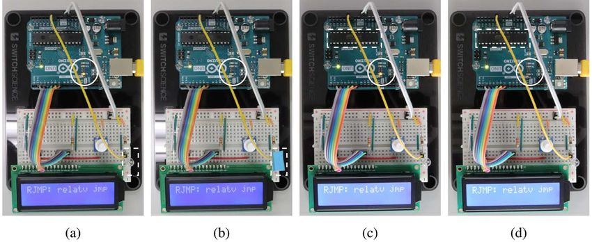
instruction of the original program. A capture of the state of the debugging sys-
tem is illustrated in Figure 8.
Next, we consider real-world sensor applications: first, we realise a simple
light sensor (photodetector) based on an HW5P-1 phototransistor. The corres-
ponding sensor control program simply turns on the LED embedded onto the
board (pin 5 of port B) when the value read by the photodetector is higher than
the threshold (see Figure 9(a)). This is achieved by connecting the phototran-
sistor to one analog pin of the microcontroller, say ADC0, and accessing the
value output by the analog-to-digital converter (ADC) that is provided by the
microcontroller. When the photodetector is covered with some opaque material,
the read value becomes smaller than the threshold and the embedded LED is not
lit (see Figure 9(b)).
Figure 7. Part of a sample injector output, notably showing the three types of
injected instructions. Besides, the original and new addresses now differ.
Figure 8. Successive photographs of the debugging system when applied to the
sample original program of Figure 4(a) (excerpt). A time indicator T (in seconds)
is given in the top left-hand corner of each photograph.
DOI: 10.4236/jst.2021.112002 29 Journal of Sensor TechnologyA. Bossard
Figure 9. Application to real-world sensors: (a, b) a photodetector and (c, d) a tempera-
ture sensor. When the value read by the phototransistor is higher than the threshold, the
embedded LED (circled) is lit (a), and otherwise not (b)—it can be noticed that the pho-
totransistor (dashed) is covered with an opaque material in the latter situation. When the
value read by the temperature sensor (dashed; included inside the microcontroller) is
higher than the threshold, the embedded LED (circled) is lit (c), and otherwise not (d).
Second, we realise a simple temperature sensor device which relies on the in-
ternal temperature sensor of the ATmega328P microcontroller (input channel
ADC8 of the microcontroller ADC). The corresponding sensor control program
simply turns on the embedded LED when the value read by the temperature
sensor is higher than the threshold (see Figure 9(c)). And when the value read
by the temperature sensor is smaller than the threshold, then the embedded LED
is not lit (see Figure 9(d)).
6. Results: Overhead Measurement
We show in this section the applicability of the proposal by formally measuring
the induced memory size and performance overheads.
First, we measure the memory size overhead that is induced by the proposed
debugging system. The values given below are in bytes. Since it depends on the
microcontroller, we define s the number of instruction types that have been
implemented in the debugging system (typically, a few dozens of instruction
types, and at most 119 [29]). The initialisation code requires a total of
372 + 18s
bytes and the step code 42 bytes. Hence, in total, the proposal debugging system
induces an overhead of
372 + 18s + 42k
bytes, where k is the number of instructions of the original program.
For reference, a microcontroller such as the ATmega328P which we used in
this experiment has 32 Kbytes (i.e. 32,768 bytes) of flash program memory (i.e.
to store the machine code). So, the following inequality must be satisfied for the
debugging system proposal to be applicable to the original program:
372 + 18s + 42k + 2k1 + 4k2 ≤ 32768
with k the number of instructions of the original program, out of which k1
DOI: 10.4236/jst.2021.112002 30 Journal of Sensor TechnologyA. Bossard
instructions are single-word and k2 double-word; so, k1 + k2 = k.
Besides, the required memory size depends on the number of original OUT
instructions to the port D as explained in Section 4.2. Given that this port is al-
most reserved for the debugging system, we can assume that the occurrence of
such an original instruction is low, so, for the sake of clarity, it is not included
in the memory size calculation below. Furthermore, we can assume without
loss of generality that the original program is made of single-word instructions
(in fact, the only instructions that are double-word are the long jumps, long calls
and very few, rather infrequent others; see for example Table 3). So, with, say,
s = 111 (111 instruction sorts, as listed in [30]), we obtain the following inequa-
lity with k the number of instructions of the original program that can be to-
lerated given the size of the program memory:
372 + 18s + 42k + 2k ≤ 32768
372 + 18 × 111 + 44k ≤ 32768
44k ≤ 30398
k ≤ 690
Yet, the value of s can be significantly reduced: a program hardly includes
all the instruction sorts. A value of s = 40 is arguably more meaningful (for in-
stance, the initialisation code and the step code of the debugging system together
merely rely on 21 instruction sorts, given in Appendix A, and moreover this
code consists of non-trivial processes, such as interfacing the LCD); it induces
k ≤ 719 . Given our assumptions, the order of the result rather than the exact
value is meaningful.
Next, we measure the performance impact of the proposed debugging system.
The values given below are counted in processor cycles, that is the number of
clock ticks required to execute the corresponding machine code. Because the
microcontroller used in this research, and thus in this experiment, is equipped
with a processor clocked at 16 Mhz, such a number of cycles can be converted in
milliseconds by dividing by 16 × 106. The initialisation code requires a total of
1,031,180 cycles.
The number of cycles required by the step code depends on t the time waited
between each instruction (for the debugging information that is displayed on the
LCD panel to be readable). In our implementation, t is a multiple of approx-
imately 1 second (1.00925 seconds, precisely), so for the sake of clarity, let us
consider simply that t is the delay in seconds. In our experiments, this delay is
set to t = 1 .
Furthermore, the number of cycles of the step code depends on whether the
corresponding original instruction is, for instance, the OUT instruction to the
port D. In such case, 22 cycles are to be added; they correspond to the additional
instructions injected as explained in Section 4.2. The same discussion is made
for the other special cases (SBRC, etc.) as mentioned ibidem. But in total, the
number of additional cycles induced by such special cases is extremely small
compared to the total, and is thus negligible. So, for the sake of simplicity they
DOI: 10.4236/jst.2021.112002 31 Journal of Sensor TechnologyA. Bossard
are not included in the following discussion.
Assuming that for each instruction sort all the sixteen characters of the LCD
panel are used to display the corresponding information, the step code requires a
total of
150601 + 16153080t
cycles. Again, this is an approximation: obviously, the magnitude of the number
of cycles rather than the exact value is relevant.
So, in total, the proposed debugging system induces an overhead of
1031180 + k (150601 + 16153080t )
cycles, where k is the number of instructions of the original program.
Inducing the most significant overhead, both memory and performance, we
give in Appendix B the details of the overhead calculations. This also shows the
step code that is injected in most cases by the proposed debugging system for
each instruction of the original program.
7. Discussion
First and foremost, the various experimental results have demonstrated that we
succeeded in realising a fully autonomous debugging system that is applicable to
any sort of program created for an AVR microcontroller. The proposal thus ef-
fectively raises the human-machine interaction usability by providing real-time,
in situ debugging information to the user, while retaining the cost of such a de-
bugging process minimal, especially compared to the conventional approach
that relies on a computer dedicated to debugging.
Furthermore, the results have shown that the proposal is applicable to sensor
devices: two effective real-world sensors (a light sensor and a temperature sensor)
were successfully realised and put to test with the proposed debugging system,
triggering an electronic signal to lighten an on-board LED when the correspond-
ing condition was satisfied.
The results of the analysis of the memory overhead induced by the proposed
debugging system on the original microcontroller program have shown that the
extra memory required stays acceptable as the debugging system can tolerate an
original program with about 700 instructions, or more depending on the opti-
mization of the debugger code.
In addition, it can be noted that the almost entirety (more than 99%) of the
cycles of the initialisation code and of the step code injected for debugging are
induced by waiting times. These waiting times are necessary especially to com-
municate with the LCD panel as per the manufacturer requirements [31] and
also to ensure a short pause between the successive debugging information out-
puts in order to avoid displaying them on the LCD panel in a too rapid manner.
Therefore, the performance overhead can be deemed less significant than the
memory overhead, especially since this overhead sort is induced almost entirely
by waiting times, and most notably (16 153 080 cycles per instruction of the
original program, which makes most of the waiting times) the delays for a short
DOI: 10.4236/jst.2021.112002 32 Journal of Sensor TechnologyA. Bossard
pause between the debugging information display outputs, and that those delays
for the pauses are adjustable to a certain extent.
Regarding the memory overhead (less significantly the performance overhead),
let us mention that it could be further reduced by using the 8-bit operation mode
of the LCD panel used in this research. This would however be a trade-off with
the number of microcontroller pins that are reserved for the debugger: the 8-bit
operation mode of the LCD panel requires twice as many data bus pins (eight
instead of four, precisely) [31].
In order to reduce the memory and performance overhead induced by the
proposed debugging system, these eight data bus pins of the LCD need to be
connected to one single port of the microcontroller so that the corresponding
values (bits) can be set in one single OUT instruction. In the case of the ATme-
ga328P microcontroller which was used in this study, this can only be the port D
and the port B as the port C provides only seven pins. And, for instance, in the
case of an Arduino Uno board, this can only be the port D since the other ports
(B and C) only provide six pins (the port B has two pins that are reserved for
other purposes and only six out the seven pins of the port C are available). This
could interfere with the bootloader though, so a fully erased, blank chip would
be needed.
8. Conclusions
Minimal power consumption is a very common requirement for sensors and
similar devices. This is the reason why they are often based on microcontrollers,
with those based on the AVR processor architecture being very popular. In addi-
tion and by definition, sensors rely on specific hardware to gather various in-
formation. Specialised hardware means specialised software development and
debugging. In this paper, we have proposed a novel approach to this issue by
describing and evaluating a fully autonomous on-chip debugging solution for
AVR microcontrollers, notably focusing on the human-machine interaction is-
sue. In other words, we have shown with a constructive proof that an autonom-
ous debugging mechanism can be implemented for sensors based on AVR mi-
crocontrollers with an optimally low—given the accessible hardware—number
of dedicated (reserved) pins (six) and a very reasonable 42-byte per original in-
struction overhead of the program memory needed for the original, debugged
program. The proposal has been validated in practice through various experiments
and its overhead formally measured.
Regarding future works, although some refinements for the proposal might be
planned, this ought to be carefully considered so that the overhead induced by
the debugging system stays minimal, as it is in this research; this is about both
the hardware (e.g. microcontroller pins) and software (e.g. memory) require-
ments. Nevertheless, possible improvements include for example simplification
of the tool chain and documentation. In addition, it would be meaningful to
analyse the portability of the proposed debugging solution to other microcon-
troller architectures.
DOI: 10.4236/jst.2021.112002 33 Journal of Sensor TechnologyA. Bossard
Funding
This research was partly supported by a Grant-in-Aid for Scientific Research (C)
of the Japan Society for the Promotion of Science under grant no. 19K11887.
Acknowledgements
The author is grateful towards the reviewers for their comments and suggestions
which helped to improve the paper. And he sincerely thanks Takeyuki Nagao
(Chiba University of Commerce, Japan) for his advices on microcontrollers.
Conflicts of Interest
The author declares no conflicts of interest regarding the publication of this pa-
per.
References
[1] Caroll, A. and Heiser, G. (2010) An Analysis of Power Consumption in a Smart-
phone. Proceedings of the 2010 USENIX Annual Technical Conference, Boston, 22-
25 June 2010, 271-284.
[2] Troglia Gamba, M., Nicola, M. and Motella, B. (2021) Computational Load Analysis
of a Galileo OSNMA-Ready Receiver for ARM-Based Embedded Platforms. Sensors,
21, 467. https://doi.org/10.3390/s21020467
[3] Rohani, A. and Zarandi, H.R. (2009) An Analysis of Fault Effects and Propagations
in AVR Microcontroller ATmega103(L). Proceedings of the International Confe-
rence on Availability, Reliability and Security, Fukuoka, 16-19 March 2009, 166-172.
https://doi.org/10.1109/ARES.2009.169
[4] Claasen, T.A.C.M. (2006) An Industry Perspective on Current and Future State of
the Art in System-on-Chip (SoC) Technology. Proceedings of the IEEE, 94, 1121-
1137. https://doi.org/10.1109/JPROC.2006.873616
[5] Chen, Y.-K. and Kung, S.Y. (2008) Trend and Challenge on System-on-a-Chip De-
signs. Journal of Signal Processing Systems, 53, 217-229.
https://doi.org/10.1007/s11265-007-0129-7
[6] Conti, G., Quintana, M., Malag, P. and Jimnez, D. (2020) An FPGA Based Tracking
Implementation for Parkinson’s Patients. Sensors (Basel), 20, 3189.
https://doi.org/10.3390/s20113189
[7] Jiang, X.Y., Lu, Y.P., Tang, H.-Y., Tsai, J.M., Ng, E.J., Daneman, M.J., Boser, B.E.
and Horsley, D.A. (2017) Monolithic Ultrasound Fingerprint Sensor. Microsystems
& Nanoengineering, 3, Article No. 17059.
https://doi.org/10.1038/micronano.2017.59
[8] Fortino, G., Giannantonio, R., Gravina, R., Kuryloski, P. and Jafari, R. (2013) Enabling
Effective Programming and Flexible Management of Efficient Body Sensor Network
Applications. IEEE Transactions on Human-Machine Systems, 43, 115-133.
https://doi.org/10.1109/TSMCC.2012.2215852
[9] Richards, P. and Debugger, A. (2018).
https://github.com/Paulware/ArduinoDebugger
[10] Simmons, S.J. (2020) UnoArduSim. Queen’s University, Kingston.
https://www.sites.google.com/site/unoardusim/home
[11] Arduino. Libraries. See the “Standard Libraries” Section.
DOI: 10.4236/jst.2021.112002 34 Journal of Sensor TechnologyA. Bossard
https://www.arduino.cc/reference/en/libraries
[12] Baker, Z.K. and Monson, J.S. (2009) In-Situ FPGA Debug Driven by On-Board Mi-
crocontroller. Proceedings of the 17th IEEE Symposium on Field Programmable Cus-
tom Computing Machines, Napa, 5-7 April 2009, 219-222.
https://doi.org/10.1109/FCCM.2009.9
[13] Bermbach, R. and Kupfer, M. (2006) Development of a Debug Module for a FPGA-
Based Microcontroller. IFAC Proceedings Volumes, 39, 275-280.
https://doi.org/10.1016/S1474-6670(17)30197-0
[14] Maier, K.D. (2003) On-Chip Debug Support for Embedded Systems-on-Chip. Pro-
ceedings of the International Symposium on Circuits and Systems, Bangkok, 25-28
May 2003, V-565-V-568.
[15] Sudeendra, K.K., Sahoo, S., Mahapatra, A., Swain, A.K. and Mahapatra, K.K. (2017)
Security Enhancements to System on Chip Devices for IoT Perception Layer. Pro-
ceedings of the IEEE International Symposium on Nanoelectronic and Information
Systems, Bhopal, 18-20 December 2017, 151-156.
[16] Hu, Y.L. and Xiong, B. (2006) Design of an Embedded On-Chip Debug Support
Module of a MCU. Proceedings of the Conference on High Density Microsystem
Design and Packaging and Component Failure Analysis, Shanghai, 27-28 June 2006,
5-8. https://doi.org/10.1109/HDP.2006.1707555
[17] Park, K., Yoo, S.G., Kim, T. and Kim, J. (2010) JTAG Security System Based on Cre-
dentials. Journal of Electronic Testing, 26, 549-557.
https://doi.org/10.1007/s10836-010-5170-y
[18] Dolinay, J., Dostlek, P. and Vaek, V. (2016) Arduino Debugger. IEEE Embedded Sys-
tems Letters, 8, 85-88. https://doi.org/10.1109/LES.2016.2619692
[19] Rahman, H. and Arefin, M.T. (2019) Design and Analysis of an Experimental Data
and Clock Multiplexing Technique for Generating Faster Single Wire Synchronous
Data Bus. Proceedings of the 2nd International Conference on Innovation in Engi-
neering and Technology, Dhaka, 23-24 December 2019, 1-5.
https://doi.org/10.1109/ICIET48527.2019.9290705
[20] Corke, P., Valencia, P., Sikka, P., Wark, T. and Overs, L. (2007) Long-Duration So-
lar-Powered Wireless Sensor Networks. Proceedings of the 4th Workshop on Em-
bedded Networked Sensors, Cork, 25-26 June 2007, 33-37.
https://doi.org/10.1145/1278972.1278980
[21] Wei, P., Ning, Z., Ye, S., Sun, L., Yang, F.H., Wong, K.C., Westerdahl, D. and Louie,
P.K.K. (2018) Impact Analysis of Temperature and Humidity Conditions on Elec-
trochemical Sensor Response in Ambient Air Quality Monitoring. Sensors, 18, 59.
https://doi.org/10.3390/s18020059
[22] Microchip Technology (2020) Microchip Studio (4. Debugging). Revision D.
[23] Stallman, R., Pesch, R., Shebs, S., et al. (2017) Debugging with GDB—The GNU Source-
Level Debugger. Tenth Edition, Free Software Foundation, Boston.
[24] Microchip Technology (2017) Microchip Debugger (MDB) User’s Guide. DS5000-
2102D.
[25] Twin Earth Software (2017) Christophe Diericx. AVRDisassembler.
https://github.com/twinearthsoftware/AVRDisassembler
[26] Sergeev, V.A. (2014) vAVRdisasm. https://github.com/vsergeev/vAVRdisasm
[27] Intel Corporation (1988) Hexadecimal Object File Format Specification. Revision A.
[28] IDA Pro. (2021) Hex-Rays. https://www.hex-rays.com/ida-pro
DOI: 10.4236/jst.2021.112002 35 Journal of Sensor TechnologyA. Bossard
[29] Microchip Technology (2020) AVR Instruction Set Manual. DS40002198A.
[30] Microchip Technology (2018) ATmega48A/PA/88A/PA/168A/PA/328/P megaAVR
Data Sheet. DS40002061A.
[31] Hitachi (1998) HD44780U (LCD-II). ADE-207-272(Z), ‘99.9, Rev. 0.0.
DOI: 10.4236/jst.2021.112002 36 Journal of Sensor TechnologyA. Bossard
Appendix A. The Instruction Sorts Used by the Proposed
Debugging System (Initialisation Code and Step Code)
As described in Section 6, the proposed debugging system can be optimised by
adjusting the supported instruction sorts upon needs. This impacts the memory
overhead induced by the debugging system. We state in Section 6 that a fraction
of all the 111 instruction sorts is generally sufficient. This is further demonstrated
in Table 1 and Table 2 which give the detail of the instruction sorts that are
present inside the initialisation code and inside the step code of the proposed de-
bugging system, respectively. In total, only 21 instruction sorts are present inside
both programs. This in addition shows the non-pervasiveness of the proposal.
Table 1. The instruction sorts present in the initialisation code injected by the proposed
debugging system.
# Instruction Description
1 andi logical AND with immediate value
2 breq branch if equal
3 brne branch if not equal
4 dec decrement
5 ldi load immediate value
6 lds load from data memory space
7 lpm load from program memory space
8 lsl logical shift left
9 lsr logical shift right
10 mov copy register
11 or logical OR
12 ori logical OR with immediate value
13 out store to I/O location
14 pop pop from the stack
15 push push onto the stack
16 rcall relative subroutine call
17 ret return from subroutine
18 rjmp relative unconditional jump
19 sts store in data memory space
20 tst test for zero or minus
Table 2. The instruction sorts present in the step code injected by the proposed debug-
ging system.
# Instruction Description
1 brne branch if equal
2 dec decrement
3 in read from I/O location
4 ldi load immediate value
5 out store to I/O location
6 pop pop from the stack
7 rcall relative subroutine call
8 push push onto the stack
DOI: 10.4236/jst.2021.112002 37 Journal of Sensor TechnologyA. Bossard
Appendix B. Details and Overhead Measurement for the
Step Code Injected by the Proposed Debugging System
As described in Section 4.2, the step code is automatically injected by the pro-
posed debugging system for (almost) each instruction of the original program
(i.e. the program that is being debugged). It is thus responsible for the majority
of the performance overhead and of the memory overhead that are induced by
the debugging system. Hence, it is meaningful to describe more in detail this
part of the proposal, and to show how the overhead was calculated.
This is summarised in Table 3. The “Cycles” column indicates the number of
cycles that are required by the instruction, whereas the “Total cycles” column
indicates the total number of cycles required when executing the step code, that
is taking into account that some instructions are executed several times because,
for instance, of loops inside the program.
Table 3. Details and overhead measurement for the step code injected by the proposed
debugging system.
# Instruction Words Bytes Cycles Total cycles
1 push r0 1 2 2 2
2 in r0, SREG 1 2 1 1
3 rcall .+CLEAR_CODE 1 2 3 79,721
4 push r31 1 2 2 2
5 push r30 1 2 2 2
6 ; ldi instruction dynamically added 1 2 1 1
7 ; ldi instruction dynamically added 1 2 1 1
8 rcall .+PRINT_CODE 1 2 3 70,856
9 pop r30 1 2 2 2
10 pop r31 1 2 2 2
11 push r16 1 2 2 2
12 push r25 1 2 2 2
13 ldi r16, 4; wait 4 times about 250 ms 1 2 1 1
14 ldi r25, 250 1 2 1 4
15 rcall .+WAIT_CODE 1 2 3 16,153,064
16 dec r16 1 2 1 4
17 brne wait_loop 1 2 1, 2 7
18 pop r25 1 2 2 2
19 pop r16 1 2 2 2
20 out SREG, r0 1 2 1 1
21 pop r0 1 2 2 2
Total 21 42 - 16,303,681
DOI: 10.4236/jst.2021.112002 38 Journal of Sensor TechnologyYou can also read