BLACK Semiconductor The Photonics Platform for any Electronic Chip - NMWP
←
→
Page content transcription
If your browser does not render page correctly, please read the page content below
2020-06-14-01
          BLACK
          Semiconductor

The Photonics Platform for any Electronic Chip

Daniel Schall - NMWP Innovation 2 GO Webinar 18.06.2020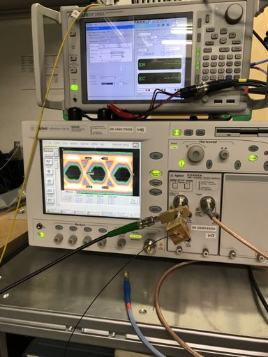
Bild: iFixit.com

                   © Black Semiconductor 2020   2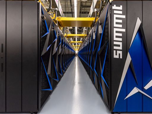
Maybe 5 more years of scaling – and then?

                                               22 nm (Intel)

Picture: TSMC

                                                   © Black Semiconductor 2020   3
Computer performance development comes to halt
                           amount of data explodes

Data curve from IDC/EMC Digital Universe reports 2008-2017, Compute curve HPE analysis,
Graphic: World Economic Forum https://www.weforum.org/agenda/2018/09/end-of-an-era-what-computing-will-look-like-after-moores-law/   © Black Semiconductor 2020   4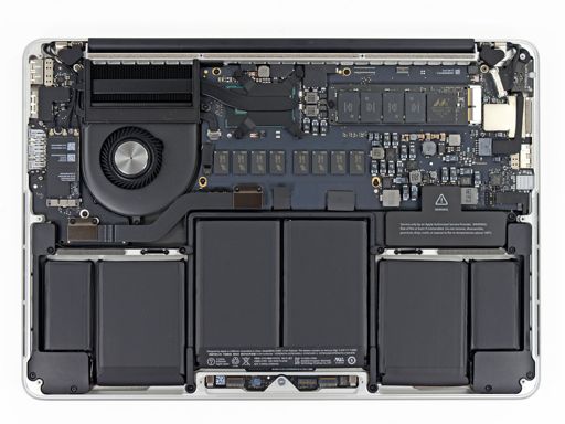
Chip design cost explode

Source: International Business Strategies (IBS)

                                                  © Black Semiconductor 2020   5
New applications - how?

       Datacenter                 5G Infrastructure
          Datarate   ↑            ↑   Datarate
             Price   ↓            ↓   Price
Energy consumption   ↓            ↓   Energy consumption

   Artificial Intelligence    Autonomous driving
        Computation speed ↑   ↑ Computation speed
       Energy consumption ↓   ↑ Datarate

                                                © Black Semiconductor 2020   6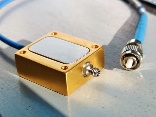
Brain vs computer

                                                        Brain                                Fastest Supercomputer: IBM Summit
      Instructions per second1                          20 x 1015                            143.5 X 10¹⁵
      Elements2,3                                       87 billion neurons                   9,216 CPUs (8 billion transistors)
                                                        100 trillion synapses                27,648 GPUs (21.1 billion transistors)
                                                        470 terabyte storage4                657 trillion transistors
                                                                                             250 petabyte storage
      Power consumption2,3                              20 Watt                              13 mega Watt

1) https://en.wikipedia.org/wiki/Computer_performance_by_orders_of_magnitude
2) https://en.wikipedia.org/wiki/Brain                                                       Billion = 109
3) https://en.wikipedia.org/wiki/Summit_(supercomputer)
4) 10.7554/eLife.10778
                                                                                             Trillion = 1012           © Black Semiconductor 2020   7
                          Pictures: www.artitout.com and Oak Ridge National Laboratory/IBM
Problem: chip IO and process speed

Today‘s electronics
needs a major upgrade!

                                        © Black Semiconductor 2020   8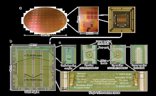
Why Photonics
Photonics enables data transfer and
processing at speed of light
Transfer speeds are a major bottleneck in computing

New applications like autonomous cars
require these faster data rates
Traditional interconnects are too slow for modern use cases

AI development is currently limited
by data transfer and process speed
Faster processing is required for unleashing AI applications                   Peng et al “Neuromorphic Photonic Integrated
                                                                               Circuits“, JSTQE 24, 6 (2018)

                                                                                   © Black Semiconductor 2020         9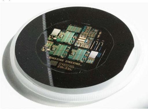
Solution: Universal 3D Photonic Platform
                            #2: photonic platform,

                              Monolithic Fabrication

                            #1: any electronic circuit,

                              Free choice of technology

                                     © Black Semiconductor 2020   10
State Of The Art: Planar CMOS & Si Photonics
Nature 556, 349 (2018)
© Black Semiconductor 2020 11Comparison: 3D vertical vs planar
New Current
Photonics: waveguide,
Graphene modulators, detectors
VIA
Planarization
on CMOS
BEOL
CMOS
Nature 556, 349 (2018)
Major difference: 3D vertical vs planar architecture
► higher performance compared to Si due to integrated graphene devices
► electronics and photonics technologically seperated
► smaller footprint due to 3D integration
► integration on any CMOS electronics, no dedicated photonics & CMOS technology
© Black Semiconductor 2020 12III-V semiconductor integration
Die attach Membrane transfer printing
Bonded
III-V dies
Si Wafer
4” Si wafer 3” III-V membrane
200 or 300 mm
Lou et al, Front. Mater., 07 April 2015 Yuqing, et al. "Indium phosphide membrane nanophotonic integrated
circuits on silicon." physica status solidi (a) 217.3 (2020): 1900606
Alternative literature:
Zhang et al. III-V-on-Si photonic integrated circuits realized using micro-transfer-
printing APL Photonics 4, 110803 (2019)
Hiraki et al. Heterogeneously integrated III–V/Si MOS capacitor Mach–Zehnder
modulator. Nature Photon 11, 482–485 2017 © Black Semiconductor 2020 13Solution: Universal 3D Photonic Platform
#2: photonic platform,
Monolithic Fabrication
#1: any electronic circuit,
Free choice of technology
© Black Semiconductor 2020 14Why Graphene Photonics?
Material Fabrication and integration
Photon
• Fast carrier dynamics: ultrafast devices
• Linear band structure: broadband devices • Fabrication on large sacle
• Low density of states: efficient devices • BEOL integration
► Ultra fast, efficient and broadband photonic devices on wafer scale
© Black Semiconductor 2020 15Device schematic
Waveguide
Graphene modulator = capacitor
Contact pads
Optical IN
detector = resistor
Optical OUT
Background: electron microscope
picture of graphene on waveguide
© Black Semiconductor 2020 16Graphene Photonics Platform
Efficient Phase Shifters
Efficient Modulators Graphene
Waveguide
Ultrafast Photodetectors
D. Schall et al., ACS Photonics 1 (9), 781-784 (2014).
D. Schall, et al., J. Phys. D: Appl. Phys., (2017).
S. Schuler et al., Nano Lett., 16 (11), 7107-7112 (2016). Contact
D. Schall et al., Opt. Express 24, 7871-7878 (2016).
M. Mohsin et al., OSA paper IM4A.1 (2015).
M. Mohsin et al Scientific Reports 5, 10967 (2015).
M. Mohsin et al., Opt. Express 22, 15292-15297 (2014).
Mohsin, Schall et al. Opt. Express 25, 31660-31669 (2017)
© Black Semiconductor 2020 17
D. Schall et al., OFC San Diego (2018).Fabrication flow
Start: Simulation Photonic layer Graphene integration
waveguide
Si waveguide
On-wafer EO Fabricated devices Graphene on Si
characterization waveguides
Graphene
devices
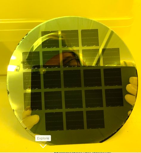
© Black Semiconductor 2020 186“ Graphene Line
100
Ω
1Ω
2048 Photodetectors on one wafer
50 Ω +/-20%: 60% OK
100 Ω threshold: 80 % OK
200 Ω threshold: 88% OK
500 Ω threshold: 90 % OK © Black Semiconductor 2020 19Proof of Concept Photodetector
Data transmission at 56 Gb/s More than 130 GHz bandwidth
5 ps
AMO and CNIT unpublished (2018) Schall et al. OFC (2018)
Data rate limited by equipment.
© Black Semiconductor 2020 20First demonstration: Graphene link @ 25 Gb/s
MZI graphene modulator
EDFA
graphene detector
AMO, CNIT, Ericsson, Nokia (Mobile World Congress 2018)
© Black Semiconductor 2020 21Photonic Platform
b)
a) Light coupling section
grating
coupler
c)
BEOL devices
waveguide
device
6” wafer with BEOL photonic
devices; mockup, no electronics
d)
© Black Semiconductor 2020 22Our Customer‘s Markets
Datacenter Chips 2025 €15 B
(Allied Market Research Jan 2019)
5G Infrastructure 2027 €45 B
(Research and Markets 2019)
AI Chip Market 2024 €27 B
(Forecast Intel 2019)
Automotive Chip Market 2025 €52 B
(Research and Markets 2018)
© Black Semiconductor 2020 23Commercial Graphene Photodetectors
Long term testing Data transmission at 14 Gb/s
Limited by pattern generator
Graphene Photodetector
© Black Semiconductor 2020 24Graphene Photodetector to be released soon
Technology Partner
                                 Applied Micro and Opto-Electronics, AMO GmbH
                                                                         Managing Directors:
                                                         Prof. Dr.-Ing. Max Christian Lemme
Key Facts                                                                Dr. Michael Hornung
•   High-Tech Research Foundry (non-profit)
                                              Key Technologies
•   Close ties to RWTH Aachen University
                                              • Silicon technology
•   500 m2 clean room
                                              • Nanofabrication (Stepper, NIL, E-Beam, IL)
•   ~60 staff members
                                              • New materials integration
                                                (high-k/metal gate, graphene, 2D
                     Key Applications           materials, perovskites)
                     • Nanoelectronics
                     • Nanophotonics
                     • Integrated sensors

                                                                    © Black Semiconductor 2020   26
AMO‘s Graphene Research Milestones
First commercial
First Top-Gate Photodetector Photodetector Graphene- Monolithic 3D
Transistor WR: 43 GHz WR: 130 GHz Photodetector Integration
Start 6“ Graphene
Graphene Photonic Pilotlinie
Start Photonics
Graphene First
reseach waveguide
photodetector
2006 2007 2009 2011 2014 2015 2017 2018 2019 2020 +
© Black Semiconductor 2020 27Acknowledgements to
contributors in the last 10 years
ALL AMO EMPLOYEES contributed at least indirectly with their knowledge and work.
Everyone contributes to keeping the cleanroom running and developing IP. Thank YOU.
Directly contributed: We would like to say thank you for giving us the opportunity to draw on 20 years of experience in CMOS,
Abbas Madani photonics, and graphene research projects at AMO in Aachen, Germany.
Abhay Sagade
Andreas Umbach
Anna Lena Giesecke
Bart Szafranek
Bartos Chmielak
Bernhard Junginger
Bernhard Wasmayr
Burkhard Grudnik
Caroline Porschatis
Christopher Matheisen
Daniel Neumaier
Galip Hepgüler
Heinrich Kurz
Holger Lerch
Martin Otto
Max Lemme
Mehrdad Shaygan
Muhammad Mohsin
Jens Bolten
Sebastian Schall
Stefan Wagner
Stephan Suckow
Thorsten Wahlbrink
Tobias Plötzing
Vimoh Shah
Wolfgang Kuebart
© Black Semiconductor 2020 28Excited?
Get in touch for further information:
CEO: Daniel Schall - daniel.schall@blacksemicon.de
+49 241 916 074 20
CFO: Sebastian Schall - sebastian.schall@blacksemicon.de
+49 241 916 074 21
© Black Semiconductor 2020 29BLACK
Semiconductor
The Photonics Platform for any Electronic ChipAdditional information
© Black Semiconductor 2020 31Waferscale Photodetector on Si SOTA
Responsivity Bandwidth Data rate Wavelength
Type
(A/W) (GHz) Gb/s nm
0.2 1480 to 1620
Graphene [1] >130 56
(gated 2 A/W) and 1980
Graphene/plasmonic
0.5 >110 100
[2]
Graphene [3] 0.36 >110 40
Ge on Si [4] 0.8 – 0.9 120 56
1) Schall et al. OFC (2018)
2) Ma et al. ACS Photonics 6, 154 (2019)
3) Ding et al. arXiv:1808.04815v3 (2018)
4) Vivien et al. Optics Express 20, 1096 (2012)
© Black Semiconductor 2020 32Absorption Modulator on Si SOTA
Modulation Attenuation Modulation/ Length Bandwidth Data rate
Type
(dB) (dB) Attenuation (µm) (GHz) Gb/s
Graphene [1] 16 3 5 300 0.7 -
(DC device)
Graphene [2] 1.3 20 0.07 120 29 50
Graphene
16 15 50 -
Simulation
Ge on Si [3] 4.6 4.1 1.1 40 >50 28
1) M. Mohsin et al. Optics Express 22, 15292 (2014)
2) Giambra et al., Optics Express 27, 20146 (2019)
3) S. Gupta et al. OFC (2015)
© Black Semiconductor 2020 33MZI Modulator SOTA
α loss VπLα BW Data rate
Modulator Type VπL (Vmm) length (µm)
(dB/mm) (dBV) (GHz) (Gb/s)
Si depletion vertical pn [1] 26.7 1.04 27.8 4000 25.6 50.1
Si depletion vertical pn [2] 7.5 2.25 16.9 2000 30.5 40
Si depletion vertical pn [3] 20 4.6 92 750 27.7 60
SISCAP [4] 2 6.5 13 400 40
III/V on Si [5] 0.9 2.6 2.3 250 2.6 32
Graphene [6] 2.8 23.6 62 300 5 10
Graphene [7] 2.7 8.7 24 RR (17µm) -
Graphene simulation [7,8] 0.8Graphene: tunable absorption
cross section 3D view Absorption in dB/µm
Absorption in dB/µm
500 nm
0.5 * Ephot
Chemical potential µc
EF 0.5*Ephot
X
§ λ = 1550 nm → Ephot = 0.8 eV
0.5*Ephot
EF § For |µc| ≥ 0.5 * Ephot states are blocked
Ephot → graphene is transparent
Absorbing Transparent
© Black Semiconductor 2020 35
M. Mohsin et al. Scientific Reports 5,10967 (2015)Tunable refractive index
cross section 3D view Effective refractive index
Effective refractive index
500 nm
0.5 * Ephot
Chemical potential
§ λ = 1550 nm → Ephot = 0.8 eV
§ Kramers-Kronig relates the absorption to the refractive index
→ refractive index is a function of the electro chemical potential
© Black Semiconductor 2020 36
M. Mohsin et al. Scientific Reports 5,10967 (2015)Absorption and Phase Modulator
cross section 3D view Effective refractive index and absorption
Effective refractive index
Absorption in dB/µm
500 nm
Phase mod Amplitude mod
§ Refractive index and absorption depend on the chemical potential
§ high mobility gives low absorption for µ < -0.4 eV
preferred for phase modulators.
Phase and absorption modulator realizable
© Black Semiconductor 2020 37
M. Mohsin et al. Scientific Reports 5,10967 (2015)Ultrafast Carrier Dynamics in Graphene
Cooling: 1.3 ps
EF
Excitation
Ephot
Heating: 50 fs
photon
Tielrooij et al Nature nanotech 10 (2015) © Black Semiconductor 2020 38You can also read