Breaking the Memory Bottleneck in Computing Applications with Emerging Memory Technologies: a Design and Technology Perspective
←
→
Page content transcription
If your browser does not render page correctly, please read the page content below
Breaking the Memory Bottleneck in
                         Computing Applications with
                       Emerging Memory Technologies:
                          a Design and Technology
                                 Perspective

M. HARRAND   CEA-LIST, LABORATOIRE INFRASTRUCTURE ET ATELIER
             LOGICIEL SUR PUCE, 17 RUE DES MARTYRS, 38000 GRENOBLE – FRANCE

G. MOLAS     CEA-LETI, LABORATOIRE DES COMPOSANTS MÉMOIRE,
             17 RUE DES MARTYRS, 38000 GRENOBLE – FRANCE

                                              2017 NVRAM Workshop | May 29-30th- 2017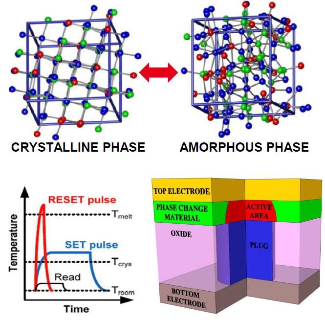
OBJECTIVES OF THIS TALK

• What are the limitations and challenges of current computing
  systems memory hierarchy ?

• What are the main emerging non-volatile memory technologies ?

• What are the main eNVM internal architectures ?

• How these emerging memories can help to solve these limitations ?
  What changes can we envisage in computing systems ?

• Which characteristics should be targeted for these memories ?

• Note : this talk focuses on computing in servers and data centers,
  not on the embedded market
                                         M. Harrand, G. Molas – NVRAM Workshop May 2017   |2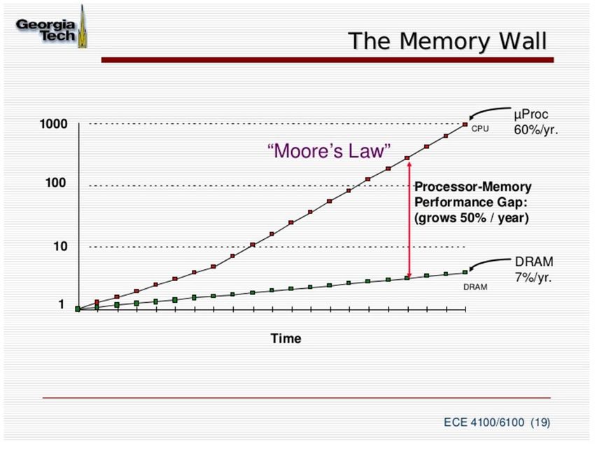
OUTLINE

Introduction

Memory hierarchy system aspects
•   Memory hierarchy
•   Limitations in computing systems,

Emerging NVM
•   Technology
•   Design

How emerging memories can help to solve current computing
systems limitations
•   Storage
•   Main memory
•   Embedded caches
•   Universal memory

Conclusions

                                                            |3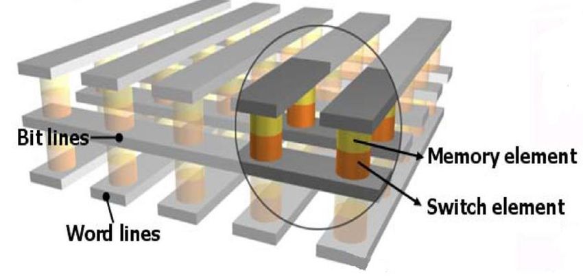
OUTLINE

Introduction

Memory hierarchy system aspects
•   Memory hierarchy
•   Limitations in computing systems,

Emerging NVM
•   Technology
•   Design

How emerging memories can help to solve current computing
systems limitations
•   Storage
•   Main memory
•   Embedded caches
•   Universal memory

Conclusions

                                                            |4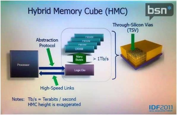
WHY A MEMORY HIERARCHY ?

• Because storage memory is far
  too slow to be used directly by the
  processor

• Processors require data to be
  accessible in ~1ns :
   •   only SRAM embedded with the
       processor are fast enough for that…
   •   but can only store small amounts of
       data

• Then, cheaper/intermediate speed
  memory – DRAM today – is used
  in between

                                             M. Harrand, G. Molas – NVRAM Workshop May 2017   |5
CURRENT MEMORY HIERARCHY ISSUES : MAIN MEMORY
• Memory wall
• Main memory bandwidth does not scale at processor bandwidth speed
Introduction to Multicore architecture
Tao Zhang – Oct. 21, 2010
• Latency
• CPU can be stuck while waiting for a cache refill
• Main memory capacity limited by the DRAM density
• frequent swap to slow storage memory
M. Harrand, G. Molas – NVRAM Workshop May 2017 |6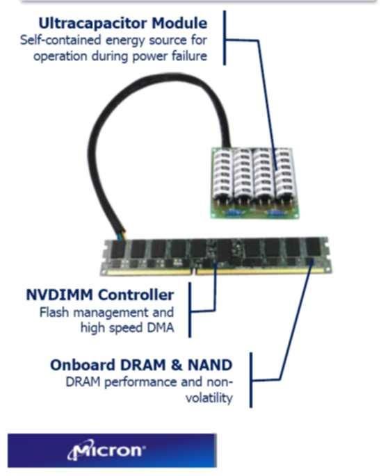
CURRENT SOLUTIONS TO MAIN MEMORY ISSUES (1/2)
• 3D stacking to increase main memory capacity
• Improve DRAM access parallelism increase the number or
banks
• DDR3 DDR4 soon DDR5
• 3D stacking increase the capacity, then the number of banks
• Improve data transfer rate
• DDR3 DDR4 soon DDR5
• HMC : logic die packet transmission bus @ 15GHz up to 320GB/s
• HBM2 : interposer very dense interconnect 1024b data bus @ 2GT/s
M. Harrand, G. Molas – IEDM 2016 SC |7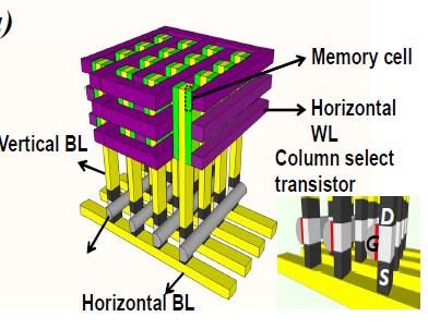
CURRENT SOLUTIONS TO MAIN MEMORY ISSUES (2/2)

•   CPU Architectural Solutions
    •   Increase cache capacity
          • But bandwidth gain is proportional to √cache capacity
          • Cache silicon area already very large

                   L2$    L2$

                   L2$    L2$

    •   Increase multithreading
          • Allows to keep the CPU busy on other tasks while waiting
              for a cache refill
          •   But supposes a higher level of program parallelization

                                            M. Harrand, G. Molas – NVRAM Workshop May 2017   |8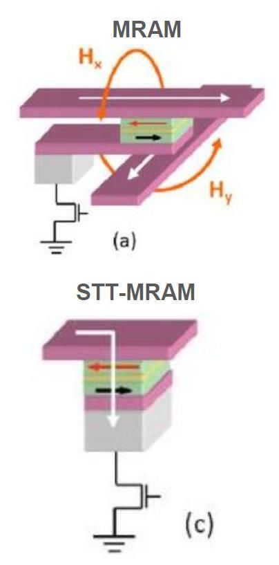
MEMORY BOTTLENECK AND GAP                        Ken Takeuchi, SSDM 2015

                                          Large gap

•   In the big data applications, the cost to transfer data among memory
    hierarchy becomes more significant

                                                M. Harrand, G. Molas – NVRAM Workshop May 2017   |9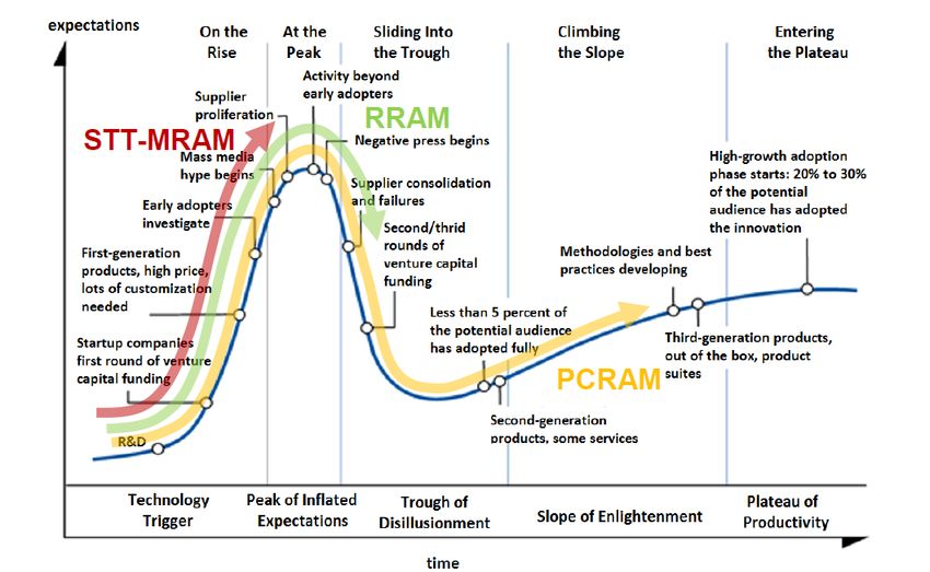
CURRENT MEMORY HIERARCHY ISSUES : STORAGE
ACCESS (1/2)
• Swap between storage and main memory
• Data integrity
• DRAM is volatile
• Periodical check-pointing is mandatory to keep data integrity even in
case of power supply loss
• Performed by OS
• In a PetaFLOP data center, these operations are forecast to use 25% of
traffic between servers and disks [Dong]
• Access to big multi-dimensional tables (big data…)
• Inefficient random access to disks
• Ex.: column access to a table that is stored by lines in the disk
• Transactional data base processing require disk access at any transaction
M. Harrand, G. Molas – NVRAM Workshop May 2017 | 10CURRENT SOLUTIONS TO STORAGE ACCESS ISSUES :
DATA BASE MANAGEMENT
• In-memory computing : put the tables entirely in DRAM
• Allows random access to tables
• But may require very large quantities of DRAM expensive!
• Mixed of DRAM and Flashes
• Ex. IBM NoSQL data server using CAPITM (Coherent
Accelerator Processor Interface) for accessing in-SSD data
bases in a coherent manner [IBM]
• DIMMs with DRAM and a back-up flash
• In case of power supply loss, DRAM data are
automatically transferred to flash
• But ~10x ordinary DIMM’s cost
• Requires a bulky battery/super-capacitor to
provide power during back-up time
M. Harrand, G. Molas – NVRAM Workshop May 2017 | 11OUTLINE
Introduction
Memory hierarchy system aspects
• Memory hierarchy
• Limitations in computing systems,
Emerging NVM
• Technology
• Design
How emerging memories can help to solve current computing
systems limitations
• Storage
• Main memory
• Embedded caches
• Universal memory
Conclusions
| 12PCM : PHASE CHANGE MEMORY • Transition between amorphous (insulating) and cristalline (conductive) state • Ge2Sb2Te5(GST) or GeTe • Phase transition of chalcogenide alloy obtained by current-induced Joule heating • Low-voltage operation(
RRAM: RESISTIVE RAM

• RRAM: formation/disruption of a conductive
  filament in a resistive layer: low/high
  resistance states
   •   OXRAM: oxygen vacancies based filament
   •   CBRAM: dissolution of an Ag or Cu active
       electrode

• Low voltage operation (~2V), fast memory
  (
MRAM: MAGNETIC RAM
• Spin-polarized current applies torque on the
magnetic moment
• 6F2 to 20F2
• Very fast (2-20ns read and write erase times,
sub ns switching reported)
• Very good endurance (>1016 cycles)
• Non volatile
• Novel interest and increased number of
papers since~ 5 years(demonstrated power
scalability through STT-MRAM)
M. Harrand, G. Molas – NVRAM Workshop May 2017 | 15EMERGING MEMORIES MATURITY LEVEL
Different levels of maturity among BEOL technologies:
•PCM most mature
•STT-MRAM at maximum peak(i.e. universal?)
•RRAM experiencing negative slope
M. Harrand, G. Molas – NVRAM Workshop May 2017 | 16BENCHMARK OF EMERGING MEMORIES
STT MRAM PCRAM CBRAM OXRAM
Scalability 20F2 4F2 4F2 4F2
MLC Spin or Small WM
3D integration PVD PVD ITRS
Fab. Cost 2015
P.
Retention 85°CARRAY ASSEMBLY IN A CROSSPOINT MEMORY
Memory cell
Resistor
Elementary memory tile
Decoder
Memory
Selector
Array
Mux / pre-amps
Memory Memory Memory Memory
Bank Bank Bank Bank
PRE-DECODER
.
Memory Memory Memory Memory
Bank Bank Bank Bank
Buffers /Transmission protocol / Control / Charge Ctrl/ AMPLIFICATION
pumps… Volt. Gen.
M. Harrand, G. Molas – NVRAM Workshop May 2017 | 183 KINDS OF MEMORY ARCHITECTURE FOR ENVRAM
[Daolin_Cai]
• 1T-1R
• Crosspoint
Samsung 2007
• VRRAM
I.G. Baek, Samsung, 2011 IEDM, p. 737.
M. Harrand, G. Molas – NVRAM Workshop May 2017 | 191T-1R
• Simple peripheral circuits :
• line drivers, sense-amps, control…
• Only possible architecture for technologies exhibiting a
too small window margin (STT-MRAM…)
• Reduced density due to the transistor
• High programming currents require big transistors
• Suitable for small to medium memories :
• embedded memories, caches…
M. Harrand, G. Molas – NVRAM Workshop May 2017 | 20CROSSPOINT ARCHITECTURE
• Very dense architecture
• Suitable for high capacity
memories
• But more constraints on the
eNVM material
M. Harrand, G. Molas – NVRAM Workshop May 2017 | 21VRRAM ARCHITECTURE
• Set of vertical crosspoint planes
• Process analog to 3D-NAND Flash
• High aspect ratio etching and conformal
deposition required
• Reduced number of masks w.r.t.
crosspoint architecture
• Cheaper than crosspoint
• For high number of layers
• But more complex process and design,
and may be slower access time
[Zhang]
M. Harrand, G. Molas – NVRAM Workshop May 2017 | 22OUTLINE
Introduction
Memory hierarchy system aspects
• Memory hierarchy
• Limitations in computing systems,
Emerging NVM
• Technology
• Design
How emerging memories can help to solve current computing
systems limitations
• Storage
• Main memory
• Embedded caches
• Universal memory
Conclusions
| 23EMERGING NVRAM CAN HELP TO SOLVE COMPUTING
SYSTEMS ISSUES
• We can think of using eNVRAM according to the following
architectures
CPU CPU CPU CPU CPU CPU CPU CPU CP CPU
L1 $ L1 $
U
L1 $ L1 $ L1 $ L1 $ L1 $ L1 $ L1 $ L1 $
L2/3 $ L2/3 $ L2/3 $ L2/3 $ L2/3 $
eNVM
Disk Disk Disk eNVM DRAM Disk
DRAM DRAM DRAM eNVM
/SSD /SSD /SSD /SSD
To other servers
A. Current B. Storage C. Main memory D. Embedded E. Universal
System Filling the gap Filling the gap memory memory
between SSD and between SSD LLC cache Main/Storage
DRAM, and DRAM …or replacement
… or SSD DRAM
replacement replacement
M. Harrand, G. Molas – NVRAM Workshop May 2017 | 24ARCHITECTURE B : STORAGE TYPE (1/3)
• Filling the gap between Flash and DRAM for Storage
CPU CPU
L1 $ L1 $
L2/3 $
eNVM
Disk DRAM
/SSD
• Ultra fast SSD, but more expensive than current flash-base ones
• Impacts on the computing system to take benefit of them:
• The network bandwidth and latency must be improved
• PCIe direct link latency ~1µs
• Enough for 100µs latency flash-based SSD, but too long for a 1µs eNVM one !
• H/W support for page management ?
• Alternatively, some computing capability may be inserted in these ultra fast
SSD (“processing in memory”) [Loh], [De]
• Key/value access
• Map functions of MapReduce algorithms,
• …
M. Harrand, G. Molas – NVRAM Workshop May 2017 | 25ARCHITECTURE B : STORAGE TYPE (2/3)
• Flash Replacement for Storage
CPU CPU
L1 $ L1 $
L2/3 $
eNVM
DRAM
• Impacts on the computing system:
• Greatly simplifies the hierarchy management
• Architecture targeted by Hewlett-Packard’s prototype “The Machine” with
photonic interconnect
[Milojicic]
M. Harrand, G. Molas – NVRAM Workshop May 2017 | 26ARCHITECTURE B : STORAGE TYPE (3/3) - TARGET
SPECS
Latency Endurance Retention Cost/b Power
Storage consumption
Filling the gap 1 – 5µs > 106 10 years @ 85°C < 2 x flash cost < flash
Replacement 1 – 5µs > 106 10 years @ 85°C ~flash cost < flash
• If used in complement with current storage solutions (“filling the
gap”), the cost can be higher than flash because it is so much
faster
• If used as a replacement, the cost must be competitive with flash,
because the storage capacity requirement of computing systems
is rising (big data…)
• RRAM or PCM in Crossbar of preferably VRRAM architecture
M. Harrand, G. Molas – NVRAM Workshop May 2017 | 27ARCHITECTURE C: MEMORY TYPE SCM (1/3)
• Filling the gap between Flash and DRAM
CPU CPU
L1 $ L1 $
L2/3 $
Disk eNVM DRAM
/SSD
• System impacts
• Simplifies data integrity management (journaling or check-pointing
schemes) [Condit], [Ren]
• Reduces check-pointing traffic
• if sufficient retention to guarantee power will be recovered before data are lost
• Transactional data base / big data applications
• Allows greater quantities of working memory
• if much denser and cheaper than DRAM
• Simplifies atomic transactions
• if sufficient retention to guarantee power will be recovered before data are lost
• Better solution than current NVDIMMs :
• no super-capacitors, higher density, cheaper
M. Harrand, G. Molas – NVRAM Workshop May 2017 | 28ARCHITECTURE C: MEMORY TYPE SCM (2/3)
• DRAM replacement
CPU CPU
L1 $ L1 $
L2/3 $
Disk eNVM
/SSD
• Same system impacts than “filling the gap”
• But much simpler to use
• Cheaper, denser
• No need for an additional logic chip to implement a HMC-like protocol
• Take opportunity of the increased capacity w.r.t. DRAM to increase data
access parallelization potential increased bandwidth
• But no improvement in latency is forecast
M. Harrand, G. Molas – NVRAM Workshop May 2017 | 29ARCHITECTURE C : MEMORY TYPE (3/3) - TARGET SPECS
Latency Endurance Retention Cost/b Power
Storage consumption
Filling the gap < 200ns > 109 > 5 days @ 85°C < ½ DRAM cost < DRAM
Replacement < 50ns > 109 * > 5 days @ 85°C < ½ DRAM cost < DRAM
* Assuming smart wear-leveling is used
• Non-volatility is not really required in this case, but retention
should be high enough to :
• Prevent refresh to cause additional wear
• Ensure data are kept long enough to recover power supply after a power
loss
• Cost must be sufficiently lower than DRAM to make this
architecture competitive
• A higher latency than DRAM one is acceptable when DRAM and
eNVM are jointly used, but not when eNVM replaces DRAM
• RRAM or PCM in crossbar architecture
M. Harrand, G. Molas – IEDM 2016 SC | 30ARCHITECTURE D: EMBEDDED MEMORY
CPU CPU
L1 $ L1 $
L2/3 $ eNVM
Disk DRAM
/SSD
• Improves last level cache density
• May improve data recovery if jointly used with eNVM main memory
• Main requirements are speed and endurance
Latency Endurance Retention Cost/b Power
consumption
< 30ns > 1016 > 5 days < eDRAM cost < eDRAM
• STT-MRAM
• However, it can be envisaged to use mixed SRAM/eNVM caches to
solve endurance issues [Wu]
• Most often written data located in SRAM, others in eNVM
M. Harrand, G. Molas – NVRAM Workshop May 2017 | 31MEMORY HIERARCHY POTENTIAL EVOLUTION : SOLUTION
E : UNIVERSAL MEMORY
CP CPU
U
L1 $ L1 $
L2/3 $
eNVM
To other servers
• No distinction between main memory and storage memory
• New OS is required to take benefits of it [Bailey]
• File systems may disappear : direct random access
• Checkpoints still necessary, but greatly simplified
• No boot : the system instantaneously restarts where you stopped it
• Drastically solves the [main memory to storage memory] bandwidth issues
• But merges DRAM and Flash requirements
Latency Endurance Retention Cost/b Power
consumption
< 50ns > 109 if smart 10 years @ 85°C ~flash cost < flash
wear-leveling is
applied
M. Harrand, G. Molas – NVRAM Workshop May 2017 | 32OUTLINE
Introduction
Memory hierarchy system aspects
• Memory hierarchy
• Limitations in computing systems,
• Current solutions
Emerging NVM performance range
How emerging memories can help to solve current computing
systems limitations
• Storage
• Working memory
• Embedded caches
• Universal memory
eNVM Design Constraints
• 1T-1R
• Crosspoint
• VRRAM
Conclusions
| 33CONCLUSIONS: MEMORY TECHNOLOGY AND DESIGN
ASPECTS
• PCM and RRAM are denser than STT-MRAM
• PCM is more mature than RRAM
• RRAM requires a lower power consumption than PCM
• STT-MRAM is faster and has a much higher endurance
• Crosspoint and VRRAM architectures are the best suited for high
density memories
• But require a high window margin, probably not compatible with STT-
MRAM
• VRRAM are promising because of the reduced cost of providing a
large number of layers
• But complex to develop
M. Harrand, G. Molas – NVRAM Workshop May 2017 | 34CONCLUSIONS : SYSTEM ASPECTS
• eNVM can be used at the following places of computer
architectures, with different spec requirements:
• Storage : between SSD and main memory or replace SSD
• Network bandwidth must increase to take benefit of it
• Main requirements : density, cost, retention PCM or RRAM, VRAM
architecture
• Main memory : on the memory bus, together with DRAM or replace DRAM
• Big benefits for big data/data base applications and on check-pointing traffic
• Main requirement : speed, density PCM or RRAM, Crossbar architecture
• Last level cache
• Increases cache density reduces memory wall issues
• Main requirements : speed, endurance STT-MRAM, 1T1R architecture
• Universal memory
• Could revolutionize OS : instantaneous boot, no files but random access to data
• But (too ?) big constraints on eNVM devices
M. Harrand, G. Molas – NVRAM Workshop May 2017 | 35REFERENCES
• [Dong] : Leveraging 3D PCRAM Technologies to Reduce Checkpoint Overhead for Future Exascale Systems
– X. Dong/HPLabs
• [IBM] : Data Engine for NoSQL – IBM Power Systems Edition – White Paper and Technical Reference
• [Loh] : A Processing-in-Memory Taxonomy and a Case for Studying Fixed-function PIM – Gabriel H. Loh et al.
• [De] : Minerva: Accelerating Data Analysis in Next-Generation SSDs - Arup De et al.
• [Milojicic] : http://fr.slideshare.net/linaroorg/hkg15the-machine-a-new-kind-of-computer-keynote-by-dejan-
milojicic
• [Condit] : Better I/O Through Byte-Addressable, Persistent Memory – J.Condit et al.
• [Ren] : ThyNVM: Enabling Software-Transparent Crash Consistency in Persistent Memory Systems – Jinglei
Ren
• [Wu] : Hybrid Cache Architecture with Disparate Memory Technologies – Xiaoxia Wu
• [Bailey] : Operating System Implications of Fast, Cheap, Non-Volatile Memory – K. Bailey et al.
• A Comprehensive Crossbar Array Model With Solutions for Line Resistance and Nonlinear Device
Characteristics - An Chen - IEEE Transactions on Electron Devices, VOL. 60, NO. 4, April 2013
• Understanding the Impact of Diode Parameters on Sneak Current in 1Diode 1ReRAM Crossbar Architectures
- Yibo Li et al.
• [Zhang]: Analysis of Vertical Cross-Point Resistive Memory (VRRAM) for 3D RRAM Design – Leqi Zhang et al.
• Non Volatile Memory Evolution and Revolution – Paolo Cappelletti IEDM2015
• Vertical CBRAM (V-CBRAM): from experimental data to design perspectives – G. Piccolboni et al. IMW2016
• [Daolin_Cai]:https://www.researchgate.net/profile/Daolin_Cai/publication/272366718/figure/download/fig4/AS:2
67505344184346@1440789652609/Figure-1-Schematic-of-the-1T1R-structure-memory-cell-b-Schematic-
cross-section-of-the.png
• [Mielke]: Bit Error Rate in NAND Flash Memories - Neal Mielke et al.
M. Harrand, G. Molas – NVRAM Workshop May 2017 | 36Thank you for
your attention
michel.harrand@cea.fr
Centre de Grenoble Centre de Saclay
17 rue des Martyrs Nano-Innov PC 172
38054 Grenoble Cedex 91191 Gif sur Yvette CedexYou can also read