EBAM 2020 3 rd International Conference on Electron Beam Additive Manufacturing 5 - 7 October 2020 Erlangen, Germany - Friedrich-Alexander ...
←
→
Page content transcription
If your browser does not render page correctly, please read the page content below
EBAM 2020
  3 rd International Conference on
  Electron Beam Additive Manufacturing
  5 – 7 October 2020 · Erlangen, Germany

www.ebam.fau.de
Welcome
It is our pleasure to welcome you to the third
International Conference on Electron Beam Ad-
ditive Manufacturing EBAM 2020, which is orga-
nized by the Chair of Materials Science and Engi-
neering for Metals (WTM) in cooperation with the
Cluster of Excellence - Engineering of Advanced Ma-
terials (EAM) at the Friedrich-Alexander-Universität
Erlangen-Nürnberg (FAU).
The conference aims to discuss specific challenges
and opportunities offered by the electron beam.
EBAM 2020 will bring together researchers and in-
dustrial users to accomplish improvements in this
technology. Invited presentations from academics as well as industry will give
high-level insight into this fabrication technology.
In the hope of a live event, we decided to postpone the conference from
March 2020 to October 2020 because of the world wide spread of the new
coronavirus. Due to the unchanged circumstances today, we came to the
conclusion, that hosting a digital EBAM 2020 with pre-recorded presentations
is the only responsible decision.
Since the first EBAM 2016, the interest in this topic has increased even further
with an enormous number of submissions from around the world. We hope
that the wide range of inspiring talks – including the invited presentations in
combination with high-quality poster presentations – initiates various fruitful
discussions in the live discussion sessions and future cooperation.
Warm thanks go to our organization team for the help and support during
preparation and the following intense days.
We are looking forward to the scientific program full of expertise from all over
the world.

Carolin Körner
Conference Coordinator
1

Table of Contents

  General Information . . . . . . . . . .     .   .   .   .   .   .   .   .   .   .   .   .   .   .   .   .   .    2
  Program . . . . . . . . . . . . . . . . .   .   .   .   .   .   .   .   .   .   .   .   .   .   .   .   .   .    4
  Oral Presentations . . . . . . . . . . .    .   .   .   .   .   .   .   .   .   .   .   .   .   .   .   .   .   10
       Mon, 5 Oct . . . . . . . . . . . .     .   .   .   .   .   .   .   .   .   .   .   .   .   .   .   .   .   10
              A1: Electron Beam . . . .       .   .   .   .   .   .   .   .   .   .   .   .   .   .   .   .   .   10
              M1: Titanium . . . . . . .      .   .   .   .   .   .   .   .   .   .   .   .   .   .   .   .   .   15
              M2: Aluminum . . . . . .        .   .   .   .   .   .   .   .   .   .   .   .   .   .   .   .   .   21
       Tue, 6 Oct . . . . . . . . . . . . .   .   .   .   .   .   .   .   .   .   .   .   .   .   .   .   .   .   24
              A2: Powder . . . . . . . .      .   .   .   .   .   .   .   .   .   .   .   .   .   .   .   .   .   24
              A3: Process . . . . . . .       .   .   .   .   .   .   .   .   .   .   .   .   .   .   .   .   .   29
              M3: Iron . . . . . . . . . .    .   .   .   .   .   .   .   .   .   .   .   .   .   .   .   .   .   35
              M4: Copper . . . . . . . .      .   .   .   .   .   .   .   .   .   .   .   .   .   .   .   .   .   39
       Wen, 7 Oct . . . . . . . . . . . .     .   .   .   .   .   .   .   .   .   .   .   .   .   .   .   .   .   43
              A4: Process Observation         .   .   .   .   .   .   .   .   .   .   .   .   .   .   .   .   .   43
              M5: Materials . . . . . . .     .   .   .   .   .   .   .   .   .   .   .   .   .   .   .   .   .   49
              M6: Nickel . . . . . . . .      .   .   .   .   .   .   .   .   .   .   .   .   .   .   .   .   .   53
  Poster Presentations . . . . . . . . . .    .   .   .   .   .   .   .   .   .   .   .   .   .   .   .   .   .   58
              P1: Poster Material . . . .     .   .   .   .   .   .   .   .   .   .   .   .   .   .   .   .   .   58
              P2: Poster Simulation . .       .   .   .   .   .   .   .   .   .   .   .   .   .   .   .   .   .   63
              P3: Poster Process . . .        .   .   .   .   .   .   .   .   .   .   .   .   .   .   .   .   .   69
2                                                     General Information

Invited Speakers
    Paolo Gennaro      Precicast Additive, Switzerland
    Matthias Gieseke   Baker Hughes, Germany
    Timothy Horn       North Carolina State University, US
    Michael Kirka      Oak Ridge National Laboratory, US
    Guilhem Martin     Science et Ingéniere des
                       Matériaux et Procédés, France
    Colin Ribton       The Welding Institute, UK
    Xipeng Tan         Nanyang Technological University, Singapore
    Julia Ureña        AIDIMME Instituto Technológico, Spain
    Wentao Yan         National University of Singapore, Singapore

Scientific Board
    Ulf Ackelid        Freemelt AB, Sweden
    Akihiko Chiba      Tohoku University, Japan
    Ryan Dehoff        Oak Ridge National Laboratory, US
    Paolo Gennaro      Precicast Additive, Switzerland
    Burkhardt Klöden   Fraunhofer IFAM, Germany
    Feng Lin           Tsinghua University, China
    Ulric Ljungblad    Freemelt AB, Sweden
    Thomas Niendorf    University of Kassel, Germany
    Lars-Erik Rännar   Mid Sweden University, Sweden
    Anders Snis        GE Additive - Arcam EBM, Sweden
    Iain Todd          University of Sheffield, UK
General Information                                    3

Conference Coordinator
 Carolin Körner           WTM, FAU Erlangen-Nürnberg

Scientific Organization
 Matthias Markl           WTM, FAU Erlangen-Nürnberg

Technical Organization
 Ina Viebach              EAM, FAU Erlangen-Nürnberg
 Michael Hartmann         EAM, FAU Erlangen-Nürnberg

Local Organization Committee
 Christoph Breuning       WTM, FAU Erlangen-Nürnberg
 Julian Pistor            ZMP, FAU Erlangen-Nürnberg
 Maximilian Wormser       ZMP, FAU Erlangen-Nürnberg
4                                                                               Mon, 5 Oct

      900 - 915    Welcome
                   Carolin Körner · FAU Erlangen-Nürnberg, Germany

      915 - 1100   Discussion on sessions A1, M1, M2 and P1
                   Chair: Matthias Markl · FAU Erlangen-Nürnberg, Germany

    A1: Electron Beam
    Electron beam guns and optics for additive manufacture
    Colin Ribton · The Welding Institute, United Kingdom
    EBMPerform – a H2020 project for developing high-quality, high-speed EBM
    3D printing by the integration of high-performance electron sources
    Joakim Ålgårdh · GE Additive - Arcam EBM, Sweden
    Open data format for beam scanning in electron beam powder bed fusion
    Robin Stephansen · Freemelt AB, Sweden
    Modelling of electron beam absorption in powders
    Benjamin Seznec · Laboratoire de Physique des Gaz et des Plasmas, France
    Technological flexibility in additive manufacturing and related processes
    provided by low voltage profile electron beam
    Dmytro Kovalchukc · JSC NVO Chervona Hvily, Ukraine

    M1: Titanium
    Titanium aluminide, 4 manufacturing processes for 1 blade
    Paolo Gennaro · GF Precicast Additive SA, Switzerland
    A study on the chemical and microstructural optimization of the Ti48-2-2 alloy
    processed by electron beam melting
    Cristian Ghibaudo · Politecnico di Torino, Italy
    Process stability and microstructural uniformity of additively manufactured
    Gamma TiAl alloy using electron beam melting
    Johnson Jacob · The University of Melbourne, Australia
    Anelastic phenomena in Ti6Al4V additivley manufactured by EBM
    Yaron Ganor · Ben Gurion University, Israel
    On the improvement of geometrical outcomes of EBM parts with a novel
    design approach
    Umut Gövez · Gazi University, Turkey
    Fatigue crack growth rate of electron beam powder bed fusion (EB-PBF)
    titanium alloy (Ti-6Al-4V): Effects of crystallographic texture
    Nik Hrabe · National Institute of Standards and Technology, United States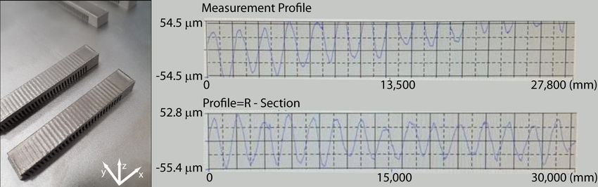
Mon, 5 Oct                                                               5

 M2: Aluminum
 Electron beam-based additive manufacturing of periodic open cellular
 Raney-Copper-Catalysts
 Zongwen Fu · FAU Erlangen-Nürnberg, Germany
 Microstructure refinement for superior ductility of Al-Si alloy by
 electron beam melting
 Huakang Bian · Tohoku University, Japan
 Selective electron beam melting of Al-Cu-Mg alloy: Processability,
 microstructure characterization, and mechanical performance
 Mohammad Saleh Kenevisi · Tsinghua University, China

 P1: Poster Material
 Please find the corresponding poster abstracts starting from page 58.
6                                                                                   Tue, 6 Oct

      900 - 1100   Discussion on sessions A2, A3, M3, M4 and P2
                   Chair: Matthias Markl · FAU Erlangen-Nürnberg, Germany

    A2: Powder
    Production and properties of gas atomized TiAl and Ti-alloy EBM-powders
    Karin Ratschbacher · GfE Metals and Materials GmbH, Germany
    Electron beam melting of alloy 718 - Powder recycling and its effect on
    defect formation
    Hans Gruber · Chalmers University of Technology, Sweden
    Influence of powder deterioration on the risk of smoke in EB-PBF processes
    using IN718 powder
    Jan Drendel · Siemens AG, Germany
    Formation mechanism, microstructure and composition of the spatter formed
    during EBM processing of IN718
    Ahmad Raza · Chalmers University of Technology, Sweden
    Modeling single-particle and powder bed absorption in CM247LC superalloy
    for electron beam melting additive manufacturing
    Guglielmo Vastola · A*STAR Institute of High Performance Computing, Singapore

    A3: Process
    Breaking the link between build temperature and powder electrical
    characteristics allows optimizing the processing window of EB additive
    Ralf Edinger · CANMORA TECH Inc., Canada
    Avoiding “smoke” with a ball milling in air for alloy powder in powder bed
    fusion type electron beam additive manufacturing
    Akihiko Chiba · Tohoku University, Japan
    Multi-physics modeling of the electron beam additive manufacturing
    processes: powder spreading, pre-heating, and melting
    Wentao Yan · National University of Singapore, Singapore
    On the Use of Inherent Strain Method for Modelling Electron Beam Melting
    Evren Tan · ASELSAN Inc., Turkey
    Development of a thermo-mechanical model of electron beam additive
    manufacturing process for repair purposes
    Fatih Sikan · McGill University Montreal, Canada
    Explore the applications of electron beam melting for industrial components
    Pan Wang · A*STAR Singapore Institute of Manufacturing Technology, Singapore
Tue, 6 Oct 7 M3: Iron SEBM processing of water atomized iron powder Alexander Kirchner · Fraunhofer IFAM, Germany Microstructural and mechanical evaluation of Cr-Mo-V cold-work tool steel produced via EBM Carlos Botero · Mid Sweden University, Sweden SEBM of wear-resistant materials Burghardt Klöden · Fraunhofer IFAM, Germany Square-celled TRIP-steel honeycomb structures produced by electron beam melting Ruben Wagner · TU Bergakademie Freiberg, Germany M4: Copper Characteristics, processing and process monitoring of high purity copper powders for EB-PBF additive manufacturing Timothy Horn · North Carolina State University, United States Effect of surface coating for pure-Cu powders on electron beam melting process Kenta Aoyagi · Tohoku University, Japan Predictive modeling and validation of electron beam powder bed fusion additive manufacturing of metals at the mesoscale Andrey Meshkov · GE Research, United States Development of CuCrZr components by electron beam melting (EBM) technology Julia Ureña · AIDIMME, Spain P2: Poster Simulation Please find the corresponding poster abstracts starting from page 63.
8                                                                           Wen, 7 Oct

      900 - 1045   Discussion on sessions A4, M5, M6 and P3
                   Chair: Matthias Markl · FAU Erlangen-Nürnberg, Germany

    1045 - 1100    Closing Remarks & Poster Awards
                   Carolin Körner · FAU Erlangen-Nürnberg, Germany

    A4: Process Observation
    Process monitoring by evaluation of backscattered electrons
    Christopher Arnold · FAU Erlangen-Nürnberg, Germany
    Bilateral detector electronic imaging technique for in-situ monitoring of
    electron beam selective melting
    Dechen Zhao · Tsinghua University, China
    In situ optical/near infrared process monitoring of selective electron beam
    melting
    Guillaume Croset · Université Grenoble Alpes, France
    Video imaging methods for in-situ detection of irregular powder bed recoating
    and hot-spots in EBM
    Marco Luigi Giuseppe Grasso · Politecnico di Milano, Italy
    Combining in-situ monitoring and X-ray computed tomography to assess the
    quality of parts by electron beam melting
    Philip Sperling · Volume Graphics GmbH, Germany
    In-situ quality inspection in Ebeam machine based on fringe projection
    profilometry
    Liam Blunt · University of Huddersfield, United Kingdom

    M5: Materials
    The role of atom probe tomography in additive manufacturing of
    engineering alloys by electron beam melting
    Xipeng Tan · Nanyang Technological University, Singapore
    Nano-structured NiAl-Cr(Mo) in-situ composites processed by
    additive manufacturing
    Andreas Förner · FAU Erlangen-Nürnberg, Germany
    Processing refractory metals by electron beam melting: Challenges and
    potentials
    Vera Jüchter · Heraeus Additive Manufacturing GmbH, Germany
    From research to production: Selective electron beam melting of a
    high wear resistant CoCrW alloy for industrial applications
    Matthias Gieseke · Baker Hughes, Germany
Wen, 7 Oct 9 M6: Nickel Data driven scan strategies for microstructure development in EBM Michael Kirka · Oak Ridge National Laboratory, United States From atoms to hot cracks in AM Ni-based superalloys: A fundamental study Guilhem Martin · Université Grenoble Alpes, France Production and properties of the single crystalline nickelbase superalloy CMSX-4 processed by SEBM Julian Pistor · FAU Erlangen-Nürnberg, Germany Modelling materials with tailored grain structures - combining grain growth models and crystal plasticity Andreas Kergaßner · FAU Erlangen-Nürnberg, Germany Tailoring thermal post-treatment for EBM produced Alloy 718 Sneha Goel · University West, Sweden P3: Poster Process Please find the corresponding poster abstracts starting from page 69.
10                                                      Mon, 5 Oct · A1: Electron Beam

     Electron beam guns and optics for additive manufacture

                                        C. Ribton
                     TWI Ltd., Granta Park, Abington, Cambridge, UK
                              e-mail: colin.ribton@twi.co.uk

Electron beams (EBs) are being deployed for two types of additive manufacturing sys-
tems – powder bed and wire fed. In powder bed systems the EB is electromagnetically
deflected to selectively melt a powder layer. In wire fed systems the beam melts a wire
to build the part.
The requirements for EBs deployed for powder bed additive manufacturing systems
present some equipment design challenges. Many systems require the EB to be
run for over 100 hours continuously, with the additional requirement that the beam
characteristics remain unchanged and manufacturing remains consistent. Compared to
EB welding machines, widely established in industry, this represents a 10 fold increase
in the gun life time. To deflect the beam across wider powder beds, allowing larger
components to be additively manufactured, a combination of high deflection angle and
long working distance is required. However, both of these features cause beam spot
aberration and can limit the resolution of the manufacturing process.
Wire fed systems may also require long beam on times when applied to larger compo-
nents. For most systems, the beam, wire feed direction, the wire position relative to
the beam and substrate and direction of movement must be orientated consistently to
maintain build performance. One EB wire fed system uses a novel electron gun design
approach to overcome these requirements.
The first additive manufacturing systems used conventional EB generators – similar
to the majority of EB welders and melters. The cathodes comprised a thin tungsten
ribbon, heated to the electron emission temperature (some 2500 ◦C) by a current
passed through it. Distortion and surface evaporation, despite changing the cathode
dimensions by only a few microns, can give rise to changes in beam intensity, and
ultimately degradation of additive manufacturing quality.
For powder bed machines, lanthanum hexaboride cathodes have been developed
which offer some distinct advantages. They are indirectly heated, using a low power
laser, and consequently can be button shaped and are more mechanically stable so
little distortion occurs. Lanthanum hexaboride emits at a much lower temperature
(1500 ◦C) so surface regression, for this material due to sublimation, is minimal.
Mon, 5 Oct · A1: Electron Beam 11
EBMPerform – a H2020 project for developing high-quality,
high-speed EBM 3D printing by the integration of
high-performance electron sources
A. Snis, J. Ålgårdh*
GE Additive - Arcam EBM, Designvägen 2, 435 33 Mölnlycke, Sweden
e-mail: joakim.algardh@GE.com
The aim of the EBMPerform project has been to overcome key obstacles concerning
future requirements for EBM 3D printing for production of complex parts through the
integration of new technologies [1]. The work has been focused on developing novel
electron beam units and integrate them with an EBM machine focusing on realising the
enhanced capabilities of consistent manufacturing performance and higher productivity.
Also, the development and integration of a new beam calibration procedure will provide
quantified quality assurance of machine manufacturing readiness. The key research
challenges have been the design of the electron source and optics, and the development
of new software for improved build procedures making best use of the new sources.
Figure 1: Parts in tool steel M4 built with the EB unit developed in EBMPerform.
[1] https://cordis.europa.eu/project/rcn/196409/brief/en?WT.mc_id=exp12 Mon, 5 Oct · A1: Electron Beam
Open data format for beam scanning in
Electron Beam Powder Bed Fusion (E-PBF)
R. Stephansen* , P. Nilsson, U. Ljungblad
Freemelt AB, Bergfotsgatan 5A, 43135 Mölndal, Sweden
e-mail: robin.stephansen@freemelt.com
A cornerstone of the worldwide R&D community is the willingness to openly exchange
data and results with peers. We introduce a modern data format for beam scanning,
Open Beam Path (OBP), designed for the specific needs of E-PBF and free for everyone
to use. With OBP, a beam scan pattern is described down to individual lines or dots.
OBP provides full freedom to define beam paths, layer by layer, and the results can
easily be shared and reused by others. OBP is free to implement with any research
equipment or software, regardless of supplier, and potentially both advanced heat
simulation software and 3D-printers can work from the same OBP file. OBP is designed
for the extremely high throughput of data needed for E-PBF, where scan speeds can
reach kilometers per second, but also for direct readability and editability desired in
R&D. To accomplish this, the OBP data format comes in two formats, one binary for
machine control and one editable text based, that are identical in respect of the data
that they can hold. A scan pattern can easily be converted between the two formats.
To generate OBP data, we have implemented a design library in Python, but as the
specifications are open, everyone is free to implement OBP into other applications.
The OBP data format will be described in detail in this presentation. We will show
examples of how to create OBP beam scan patterns and illustrate the results by videos
of beam patterns recorded in a Freemelt ONE E-PBF system [1].
Figure 1: An example of a beam scan pattern (left) and its corresponding code (right).
[1] U. Ljungblad, U. Ackelid, P. Ohldin, R. Stephansen, M. Wildheim, EBAM 2018, Nuremberg.Mon, 5 Oct · A1: Electron Beam 13
Modelling of electron beam absorption in powders
B. Seznec* , T. Minea
LPGP, Laboratoire de Physique des Gaz et des Plasmas, UMR 8578, CNRS, Univ. Paris-Sud,
Université Paris-Saclay, Orsay CEDEX, 91405, France
e-mail: benjamin.seznec@u-psud.fr
Among the processes used for additive manufacturing, Electron Beam Melting (EBM)
is an interesting method to produce metallic structures layer by layer from metal powder
because due to the higher available power of the electron beam (10 kW) compared
to CW lasers (< 1 kW). In addition, while the penetration distance of the laser into a
powder particle is limited by the skin effect (maximum 100 nm), the electron beam can
penetrate deeper (ten micrometers) into the powder particle, depending of its kinetic
energy, and hence heating it uniformly and more efficient. However, the powders
accumulate electrons (depending of its electrical conductivity) and cause them to repel
each other. Under several conditions, the electrostatics forces can become so strong as
the powder particles are ejected from the powder bed — phenomenon called smokes.
It is therefore necessary to understand electron transport to optimize powder heating
and minimize powder charging effects due to electron penetration into metal powders.
The energy transferred to the metal and inelastically loss by other mechanisms is an
important issue.
A model describing the trajectory of electrons inside one powder particle has been
developed by LPGP. Electron collisions are treated using Monte Carlo method and the
energy loss of the electrons can be deduced from the stopping power of the electron
into the metal. It consider also the generation of secondary electrons, especially at the
border of the particles. In addition this model, deals with the electron backscattering
in the case of a powder bed layer and allows the estimation of the volumic density of
power released by electrons to the powder.
This presentation will figure out the general behavior of electron absorption giving the
parametric trends in relation to with the powders radius, energy of the electron beam,
beam shape etc. The aim is to quantify the deposited energy on the powder bed and
estimate the heating and the charging of the powder particles.14 Mon, 5 Oct · A1: Electron Beam
Technological Flexibility in Additive Manufacturing and Related
Processes Provided by Low Voltage Profile Electron Beam
D. Kovalchuk* , V. Melnyk, I. Melnyk, B. Tugai
JSC NVO Chervona Hvilya, 28 Dubrovytska str., Kyiv 04114, Ukraine
e-mail: dmytro@xbeam3d.com
For a long time the electron beam is considered as the most flexible heating source
in metallurgy, allowing precise control of both power and power concentration over
a wide range. In additive manufacturing – both in PBF and DED processes – EB
guns developed for welding are mainly used, often with only minor changes in the
design and in the beam control methods. The electron beam generated by such EB
guns has a relatively low total power, but a very small focal spot, which results in quite
high energy concentration - up to 106 W/cm2 . At the same time, during layer-by-layer
formation of a three-dimensional object the energy of the heating source should be
released in a very small volume of the processed material, and the melting depth
should be minimized to avoid damaging the previously deposited layers. In DED-wire
processes, typical parameters of the welding EB gun make it even more difficult to
control the energy distribution between the substrate and additive material, resulting
in low accuracy and coarse metal structure of the produced parts. Gas-discharge
electron beam guns are able to solve most of these problems thanks to their capability to
generate low voltage (Mon, 5 Oct · M1: Titanium 15
Titanium Aluminide, 4 Manufacturing Processes for 1 Blade
P. Gennaro
GF Precicast Additive SA - Via Gaggiolo, 27 6855 Stabio, Switzerland
e-mail: paolo.gennaro@georgfischer.com
TiAl manufacturing is one of the most challenging operations in the additive world, and
the EBM process is today the only practical way to do. The LPT blade is probably
the most important industrial application using TiAl and the EBM process. The aim
of the presentation is to explain why the EBM additive process represent the most
cost-effective solution compared with Casting, Forging and Milling from a block.
Figure 1: 4 Manufacturing Processes for TiAl blades.16 Mon, 5 Oct · M1: Titanium
A study on the chemical and microstructural optimization of the
Ti48-2-2 alloy processed by Electron Beam Melting
M. Galati1,3,* , C. Ghibaudo2,3 , G. Rizza1 , R. Wartbichler4 , S. Mayer4 , L. Iuliano1,3 ,
H. Clemens4 , D. Ugues2,3 , S. Biamino2,3
(1) Department of Management and Production Engineering,
Integrated Additive Manufacturing (IAM) Centre, Politecnico di Torino, Italy
(2) Department of Applied Science and Technology,
Integrated Additive Manufacturing (IAM) Centre, Politecnico di Torino, Italy
(3) Consorzio Interuniversitario Nazionale per la
Scienza e Tecnologia dei Materiali (INSTM), Italy
(4) Department of Materials Science, Montanuniversität Leoben, Austria
e-mail: manuela.galati@polito.it
Engineering titanium aluminide (TiAl) alloys are a family of intermetallic materials
that, thanks to their outstanding specific mechanical properties, attracted significant
attention for high-temperature automotive and aerospace applications. One of the
key-points for the introduction of TiAl alloys as jet turbines for the next generation of
aircraft engines is related to the sustainable weight reduction. Electron Beam Melting
(EBM) already proved to be a promising process for TiAl alloys production, however
further efforts are necessary in the comprehension of the role of the process param-
eters in order to better understand their relationship with residual porosity, Al loss
and homogeneity of the microstructure. In order to improve the final properties, in
this work a study of the EBM process as well as the subsequent heat treatment has
been carried out on Ti-48Al-2Cr-2Nb (at. %) alloy and two slight modified chemical
compositions. Theoretical-experimental analysis has been combined with the use of
simulation tools to speed up the optimisation of both chemical composition and process
parameters for EBM production. Such a combined approach was conducted regarding
the influence of Al loss during the EBM process on phase fraction and phase transition
temperatures. Additionally, heat treatment studies were carried out to further optimize
the microstructure.
The presented work summarizes the preliminary results obtained in the NEWTEAM
project “Next gEneration loW pressure TurbinE Airfoils by aM” funded by the EU’s
Horizon 2020 programme in the framework of Clean Sky 2.
Figure 1: Microstructure and process parameter optimisation by process simulation tool: Effects
of the process parameters on the aluminum loss and porosity.Mon, 5 Oct · M1: Titanium 17
Process stability and microstructural uniformity of additively
manufactured Gamma TiAl alloy using Electron Beam Melting
J. Jacob1,* , D. Fraser2 , S. Gulizia2 , K. Xia1
(1) Department of Mechanical Engineering, The University of Melbourne, Victoria 3010,
Australia
(2) CSIRO Manufacturing, Private Bag 10, Clayton South MDC, VIC 3169, Australia
e-mail: jacobj1@student.unimelb.edu.au
Ti–48Al–2Cr–2Nb alloy was manufactured by the electron beam melting (EBM) process,
microstructural development and process stability were investigated. The requirement
of high build temperatures 1000 °C for crack free TiAl printing is a challenge for a
stable process, primarily due to the electron beam nature of the heat input and the
electrical overcharging of the powder bed. Preheating and printing strategy using pins
were helpful for adequate sintering of the powder bed, thereby reduced the occurrence
of charge build-up and powder smoke. It is generally recognised that as-EBM TiAl
samples exhibit a microstructural banding along the build direction, which can be
attributed to the cyclic heat input and local Heat Affected Zones (HAZ) during layer
by layer deposition in EBM [1]. Nearly fully dense Ti-48Al-2Cr-2Nb samples with
minimum defects were printed. Detailed microstructural characterization along the
build direction of samples printed by EBM showed that Energy Density (ED) has
considerable influence on the as-EBM microstructure and final build quality in the EBM
process. The microstructural uniformity along the build direction has been studied
under different energy input conditions. Higher energy input, ED 6 J/mm 2 or more,
showed better uniformity. Higher energy samples were near lamellar but medium
and low energy samples were duplex or featureless massive gamma structure. 30%
increase in colony size was observed with an increase of ED from 4 J/mm2 to 6 J/mm2 .
The study provides a valuable reference for fabricating gamma TiAl parts by EBM and
control of microstructural uniformity.
[1] Todai, Mitsuharu, et al. (2017) Additive Manufacturing, 13, 61-70.18 Mon, 5 Oct · M1: Titanium
Anelastic Phenomena in Ti6Al4V Additivley Manufactured by
Electron Beam Melting
Y. I. Ganor1,2,3,* , E. Tiferet1,2 , M. Chonin2 , A. Garkun4 , S. Samuha1 ,
R. Z. Shneck3 , O. Yeheskel5
(1) Nuclear Research Center-Negev, P.O. Box 9001, Beer-Sheva 84190, Israel
(2) Rotem Industries, Additive Manufacturing Center, Rotem Industrial Park, Israel
(3) Ben Gurion University, Department of Materials Engineering, Beer Sheva, Israel
(4) Israel Institute of Metals, Technion R&D Foundation, Technion City, Haifa, Israel
(5) Materials Consultant, Shoham, Israel
e-mail: yaronganor87@gmail.com
Additive Manufacturing (AM) of metals is becoming a widespread method for fabricating
parts in many industries. As a relatively new method, AM parts and methods are
constantly being tested and improved. Mechanical properties are the focus of intensive
studies, along with optimization of printing parameters and processes. Under certain
service conditions, mechanical properties may be altered (i.e. cyclic loading), raising
concern to their applicatibility. Therefore, while designing an engineering part for
prolonged service, aspects such as anelastic phenomena (relaxation, hysteresis or
creep for instance), should be considered.
This study is focused on anelastic phenomena and their implications on the mechanical
properties of the Ti6Al4V additively manufactured products via electron beam melting.
Printed specimens were subjected to symmetric cyclic tension/compression loading
in the elastic regime and relaxation tests were also performed. Post processes on
printed specimen were compared with commercially available extruded specimens.
Results showed that the AM specimens exhibit different anelastic properties compared
to extruded specimens, most likely as a result of the unique microstructure of AM parts,
including hysteresis. It was also shown that specimen groups, differing by the post
processing treatment had different stress coping mechanisims, resulting in changes in
the material and mechanical properties.Mon, 5 Oct · M1: Titanium 19
On The Improvement of Geometrical Outcomes of EBM Parts
with a Novel Design Approach
U. Gövez1,2,* , O. Yilmaz2 , E. Tan1 , B. Gümüş1
(1) ASELSAN Inc., Yenimahalle, 06370, Turkey
(2) Advanced Manufacturing Technologies Research Group,
Department of Mechanical Engineering, Gazi University, Maltepe, 06570, Ankara, Turkey
e-mail: ugovez@aselsan.com.tr
Additive Manufacturing (AM) recently presents an increasing growth regarding the
production of mechanical parts, due to its outstanding characteristics in comparison
to conventional processes. AM methods facilitate the production of parts with unique
and complex geometries without requiring subsequent operations or processes [1].
Electron beam melting (EBM) is considered as one of the effective AM methods to
production of metallic parts. Designers are mostly unaware of the capabilities of EBM
method and they face many challenges to utilize the EBM process because of the
lack of design rules and guidelines [2]. Geometrical tolerances are very critical for
a functional component and the manufacturing process plays an important role to
determine the tolerances. Therefore this study aims to investigate the relationship
between neighbouring features and productability of parts with improved geometric
tolerance by using EBM. The goal was to propose specific design rules for these
features. Hence, an experimental artifact (Figure 1) including different feature groups
mainly composed of holes with / without dummy cylinders has been designed The
holes and cylinders were modelled with different interspacing from 130 to 500 µm to
examine the effect of geometric tolerances. The artifact from Ti6Al4V powders was
produced with an ARCAM A2X machine and investigated.
The results have shown that by using EBM method with dummy cylinders; geometrical
tolerances were improved, surface roughness (Ra) were decreased down to 17 µm,
dimensional accuracies were improved by more than 50 % compared to EBM catalogue
capability and 30 % better cylindiricity-circularity was obtained.
Figure 1: EBM Test Artifact.
[1] Umaras, Eduardo, and Marcos SG Tsuzuki (2017) IFAC-PapersOnLine, 50(1), 14940-14945.
[2] Ameen, Wadea, Abdulrahman Al-Ahmari, and Osama Abdulhameed (2019) "Design for Metal
Additive Manufacturing: An Investigation of Key Design Application on Electron Beam Melting".20 Mon, 5 Oct · M1: Titanium
Fatigue Crack Growth Rate of Electron Beam Powder Bed
Fusion (EB-PBF) Titanium Alloy (Ti-6Al-4V): Effects of
Crystallographic Texture
N. Hrabe* , J. Benzing, T. Quinn, L. Koepke, J. Splett
National Institute of Standards and Technology (NIST), Material Measurement Laboratory,
Boulder, CO, USA
e-mail: nik.hrabe@nist.gov
The effects of crystallographic texture and internal pores on ASTM E647 fatigue crack
growth rate (R = 0.1) of electron beam powder bed fusion (EB-PBF, Arcam A1) tita-
nium alloy (Ti-6Al-4V) were investigated by studying material in the as-built and hot
isostatically pressed (HIPed) conditions as well as in two orthogonal crack growth
directions with respect to the build direction. HIPing sufficiently reduced porosity (x-ray
CT), and unexpected texture variation (EBSD) was observed for this material (i.e. NOT
β -fiber in the build direction). It is hypothesized that the Arcam scan length
function (at scan lengths shorter than the lack-of-fusion formation limit) unintentionally
leads to variations in melt pool aspect ratio and gives rise to significant texture variation,
possibly for identical parts adjacent to each other in the same build. Significant effect
on the onset of unstable crack growth was observed due to internal porosity and texture
variation.Mon, 5 Oct · M2: Aluminum 21
Electron Beam-Based Additive Manufacturing of Periodic Open
Cellular Raney-Copper Catalysts
Z. Fu1,* , T. Wolf1 , J. Ye1 , C. Körner1,2
(1) Joint Institute of Advanced Materials and Processes, Friedrich-Alexander-Universität
Erlangen-Nürnberg, Dr.-Mack-Straße 81, 90762 Fürth, Germany
(2) Chair of Materials Science and Engineering for Metals, Friedrich-Alexander-Universität
Erlangen-Nürnberg, Martensstrasse 5, 91058 Erlangen, Germany
e-mail: zongwen.fu@fau.de
The powder bed-based selective electron beam melting (SEBM) is so far considered the
optimal approach to fabricate periodic open cellular structures (POCS) for applications
in chemical reaction engineering. In this work, Raney-Copper POCS with dense struts
composed of a highly brittle Al-Cu alloy containing 29.4 at.% copper are successfully
processed via SEBM (Figure 1 (a)). After selective leaching of aluminum in a NaOH
solution, catalytic active periodic open cellular structures (CAPOCS) containing core-
shell structured struts with a nanoporous copper surface layer and a solid core are
derived (Figure 1 (b)). The SEBM-processed and selectively leached Raney-copper
CAPOCS show a high catalytic activity in methanol synthesis. The nanoporous skin
layer exhibits a high reaction surface area, while the unreacted core ensures sufficient
mechanical stability for the reactor application and improves heat transfer.
Figure 1: (a): CT-cutaway reconstruction of a SEBM-processed POCS with dense struts in the as-
build state; (b): microstructure of the cross section of a leached strut with a nanoporous copper
skin layer and a solid core; the inset shows copper ligaments and channels in the nanoporous
skin area.22 Mon, 5 Oct · M2: Aluminum
Microstructure refinement for superior ductility of Al–Si alloy by
electron beam melting
H. Bian1,* , K. Aoyagi1 , Y. Zhao1 , C. Maeda2 , T. Mouri2 , A. Chiba1
(1) Institute for Materials Research, Tohoku University,
2-1-1 Katahira, Aobaku, Sendai 980-8577, Japan
(2) Production Engineering Development Div., Toyota Motor Corporation,
1 Toyota-cho, Toyota, Aichi 471-8571, Japan
e-mail: bianhuakang@imr.tohoku.ac.jp
Refining the Si phase in Al–Si alloy has been a research interest for decades. Previous
studies suggested many Al- and Si-enriched nano-segments (approximately 100 nm)
can coexist in a melted Al–Si liquid solution when they were reheated to a temperature
between 1080 and 1290 ◦C. These nano-segments could be retained to become crystal
nuclei and grew into fine grains under a very fast cooling rate. Thus, this provides a
novel approach of refining the microstructure of Al–Si alloy using electron beam melting
(EBM) technology because the temperature exceeds 1500 ◦C in the melting pool with
a cooling rate higher than 103 ◦C s−1 during EBM building process. In this study, EBM
is used to refine the microstructure of AlSi10Mg alloy to enhance the ductility. The
formation mechanism of the microstructure during EBM build process was discussed.
An argon gas-atomized AlSi10Mg (wt %) powder was used to fabricate as-built speci-
mens using an Arcam A2X EBM system (Arcam AB, Mölndal, Sweden). AlSi10Mg al-
loys with well surface finish were fabricated using EBM. The microstructure observation
shows mixed fine island-like and scattered granular Si phase particles (approximately
2 µm) having rounded corners and edges were embedded in the Al matrix. Fine Al
sub-grains with size of 0.5 to 2 µm formed during EBM building process. A maximum
ductility of approximately 32.7 % with a tensile strength of approximately 136 MPa were
achieved for the as-EBM-built AlSi10Mg alloy [1]. The improved ductility compared with
cast ones was attributed to the fine Si phase and the bimodal Al grains (large and fine
sub-grains). A novel pathway of refining the Al–Si alloy microstructure to improve the
tensile ductility without adding any modification element was developed in this study.
[1] H. Bian et al. Additive Manufacturing (2019) in press.Mon, 5 Oct · M2: Aluminum 23
Selective electron beam melting of Al-Cu-Mg alloy:
Processability, Microstructure Characterization,
and Mechanical Performance
M. S. Kenevisi1,2,* , F. Lin1,2
(1) Department of Mechanical Engineering, Tsinghua University, Beijing 100084, China
(2) Bio-Manufacturing and Rapid Forming Technology Key Laboratory of Beijing,
Tsinghua University, Beijing 100084, China
e-mail: kenevisims10@mails.tsinghua.edu.cn
Additive manufacturing of meal parts has been widely considered in different industries
recently. To date, the most commonly used Al alloys for AM are eutectic/near-eutectic
alloys. However, fabricating high strength aluminum parts have not yet fully investigated
due to their susceptibility to solidification cracking and porosity formation. Compared
with the selective laser melting, electron beam selective melting (EBSM) provides high
potential for fabrication of aluminum alloys as is not affected by reflectivity of metal
powders along with the advantage of oxidation inhibition in vacuum.
Gas atomized Al2024 powder was used in this study. Different sets of processing
parameters such as beam current, scanning speed, hatch spacing, and scan strategy
were used to investigate their effect on the parts’ performance. Samples with relative
densities ranges from 95 % to full-dense were built and results showed high relative
densities can be achieved by increasing the input energy to an optimum value, however
by further increasing the energy the relative density decreases as a result of porosity
formation. As shown in Figure 1, crack-free, equiaxed and fine-grained microstructure
mainly having eutectic Al2Cu and AlCuMnFe phases distributed in α phase matrix was
obtained.
Microhardness results showed an almost uniform change of hardness values in both
horizontal and vertical sections, ranges from 100 HV to 110 HV for as-built sam-
ples. Moreover, tensile and yield strengths of as-built samples reached 314 MPa and
192 MPa, respectively.
Figure 1: SEM micrograph of an as-built sample displaying defect-free microstructure.24 Tue, 6 Oct · A2: Powder
Production and Properties of Gas Atomized TiAl and
Ti-alloy EBM-Powders
K. Ratschbacher1,* , J. Lindemann2 , M. Allen1 , V. Güther1
(1) GfE Metalle und Materialien GmbH, Nuremberg, Germany
(2) GfE Fremat GmbH, Brand-Erbisdorf, Germany
e-mail: karin.ratschbacher@gfe.com
EBM-technology (Electron beam melting) has lead to an increased demand of TiAl-
and Ti-powders. Among the applicable atomization technologies, the EIGA processing
(Electrode Induction Gas Atomization) provides a reasonable set of melting and atom-
izing parameters for adjusting the resulting particle size distributions to the different
AM technology needs.
TiAl based as well as tailor made Ti-alloy EIGA electrodes are being produced via
single step VAR processing (Vaccum Arc Remelting) and subsequent VAR Skull Melting
followed by centrifugal casting [1] or gravity casting [2] in permanent moulds. Typical
diameters are in the range of 80 to 120 mm. EIGA processing principle shown in
Figure 2 offers a crucible free melting procedure which saves energy and prevents
very effectively the pick-up of metallic or ceramic impurities. Controlled Ar-atmosphere
throughout all post-atomization powder handling steps minimizes pick-up of impurities
during sieving and packaging.
Physical powder properties such as sphericity, Ar porosity, particle size distribution,
apparent density and flowability depend on gas atomization parameters namely the
nozzle diameter, the Ar flow rate, the melt rate and the corresponding shape of the
induction coil. Within a given frame it is possible to adjust the atomizing parameters
to different requirements on the particle size distribution in order to optimize specific
powder yields to subsequent processing via EBM.
The fast-growing demand for spherical TiAl powders requires further efforts for tech-
nology improvements. One of the key steps to increase the efficiency is to maximize
powder yields for the target grain size distribution, while not compromising key physical
powder properties.
Figure 1: Sketch of EIGA process and resulting TiAl48-2-2 powder for EBM.
[1] V. Güther, M. Allen, J. Klose, H. Clemens (2018) Intermetallics, 103, 12-22.
[2] K. Ratschbacher, J. Lindemann, M. Allen, V. Güther (2019) Intermetallics, 104.
[3] V. Güther, K. Ratschbacher, J. Lindemann (2019) Manufacturing of TiAl Powders Based on
Electrode Induction Gas Atomization, presentation at the Titanium Europe 2019, Vienna, Austria.Tue, 6 Oct · A2: Powder 25
Electron Beam Melting of Alloy 718 - Powder Recycling
and its Effect on Defect Formation
H. Gruber* , E. Hryha, L. Nyborg
Chalmers University of Technology, Rännv. 2A 41296 Gothenburg, Sweden
e-mail: hans.gruber@chalmers.se
This study addresses the connection between powder recycling, powder chemistry and
presence of defects in EBM processed Alloy 718. First, virgin and recycled powder was
studied to detect differences in surface morphology, surface chemical composition as
well as bulk chemistry as a consequence of powder recycling. Significant oxidation of
the powder surface is observed to occur during long-time exposure at the conditions in
the EBM build chamber, leading to a steady gain in oxygen level of the progressively re-
used powder [1]. Following this, analysis of the EBM material processed from recycled
powder shows that the amount of oxide inclusions is clearly higher than in the virgin
powder counterpart. In addition, large lack of fusion defects (LOFDs) form more easily
when using the recycled powder, owing to accumulation of oxide in the hatch-contour
interface region, as well as due to the reduced conductivity of the oxidized powder.
Based on the defect morphologies, it is shown that most defects originate from Al-rich
oxide particulates from the surface of the recycled powder, as well as titanium nitride
from inside the powder, see Fig. 1. Clustering of oxide and nitride in the liquid metal
often results in large inclusion defects. Elimination of porosity and LOFDs through hot
isostatic pressing (HIP) of the as-printed specimens clearly reduces the defect density.
However, as compared the virgin powder counterpart, the samples produced from
recycled powder have a higher defect density after HIP treatment due to the higher
amount of oxide inclusions [2].
Figure 1: Transfer of non-metallic inclusions from the powder to the component in EBM process-
ing.
[1] H. Gruber, M. Henriksson, E. Hryha, L. Nyborg (2019) MMTA, 50, 4410-4422.
[2] H. Gruber (2019) Electron beam melting of Alloy 718 – Powder recycling and its effect on
defect formation, Licentiate Thesis, Chalmers University of Technology.26 Tue, 6 Oct · A2: Powder
Influence of powder deterioration on the risk of smoke in
EB-PBF processes using IN718 powder
J. Drendel1,* , F. Heinrichsdorff1 , L. Logvinov2 , K. Hilgenberg2
(1) Siemens AG, Siemensdamm 50, 13629 Berlin, Germany
(2) Bundesanstalt für Materialforschung und -prüfung, Unter den Eichen 87,
12205 Berlin, Gemany
e-mail: jan.drendel@siemens.com
Using electrons as energy source in powder bed fusion additive manufacturing brings
a number of advantages, but also leads to charging of the powder particles. Due to the
high electric resistivity of powder beds the electrostatic forces can reach the magnitude
of the particles gravitational forces and lift the particles out of the build plane. This
event, often referred to as "smoke" or "powder spreading", destroys the current powder
layer and may lead to process termination. In this work, a procedure was developed to
determine smoke free process windows for electron beam current and scan velocity,
including the influence of a repeating scan pattern. Investigations have been conducted
using Inconel 718 powder. It has been shown, that for an arbitrary scan pattern and a
fixed beam current, the scan velocity not only has a lower limit but also an upper limit.
Exceeding either leads to smoke. While the reason for the lower limit is obvious, the
upper limit is counter-intuitive as a higher scan velocity leads to a more even charge
deposition across the powder bed. Investigations were repeated for three different
levels of powder aging. With increasing powder age, the velocity window decreases.
For unaged powder, the velocity limits did not show a significant dependence on the
electron beam current, which cannot be explained using prevailing models for powder
bed charging.
Figure 1: Determination of the process window for different scan patterns.Tue, 6 Oct · A2: Powder 27
Formation mechanism, microstructure and composition of the
spatter formed during EBM processing of IN718
A. Raza* , S. Cao, E. Hryha
Department of Industrial and Materials Science, Chalmers University of Technology,
SE-412 96 Gothenburg, Sweden
e-mail: ahmadra@chalmers.se
Considering the recyclability of the powder, there are two major factors which can
immensely deteriorate the properties of the final product that include powder surface
oxidation and spatters formation. The powder oxidation of IN718 has been studied
already presented [1-2]. However, the spatters analysis did not attract enough attention.
The current study is focused on the investigation of the spatter formation during EBM
processing of IN718. For the analysis of the spatters, heat shields from Arcam A2X
machine were used which contains a large density of the condensate with presence of
spatter particles, see Fig.1. Hence, the evaporation and condensation of the elements
with high vapor pressure were also studied. Microstructural and chemical analysis have
been done by using HRSEM, EDS, XPS and AES techniques. The spatter distribution
analysis on the sheet shows that most of the spatter is located at the bottom of the
heat shields, assuming high fraction of the spatter present in the powder bed. Spatter
observed on the heat shields is covered by layer of condensate, deposited after spatter
deposition. The chemical analysis of the powder surface and corss-section by EDS
and XPS have shown that the surface of the spatters on the heat shield mainly covered
by the oxides of Al and Cr, corresponding to the higher thermodynamic stability of the
mentioned oxides.
Figure 1: The illustration of spatter distribution on the heat shields.
[1] H. Gruber, M. Henriksson, E. Hryha and L. Nyborg (2019) MMTA, 50, 4410-4422.
[2] H. Gruber (2019) Licentiate Thesis, Chalmers University of Technology.28 Tue, 6 Oct · A2: Powder
Modeling single-particle and powder bed absorption in CM247LC
superalloy for electron beam melting additive manufacturing
W.-J. Ding, G. Vastola* , Y.-W. Zhang
A*STAR Institute of High Performance Computing, 1 Fusionopolis Way 16-16, Singapore
138632, Singapore
e-mail: vastolag@ihpc.a-star.edu.sg
Precise representation of electron-matter interaction is crucial to accurate modeling of
the electron beam melting process, especially given the high energies at play compared
to laser processing. For industrially-relevant alloys such as CM247LC, electron beam
melting is a promising candidate to tackle the significant challenge of building a crack-
free component. With this long-term goal in mind and starting with established semi-
empirical models for pure metals, we study electron beam absorption for the actual alloy
composition of CM247LC. Using the model, we then simulate absorption in one particle
and in a powder bed. Single-particle absorption profile is consistent with validated
single-element profiles. Absorption in powder bed clearly shows the front particles
shadowing the buried ones, thus providing a complex absorption landscape. In turn,
energy absorption profile is a key ingredient for a reasonable model of heat source for
the electron beam process.Tue, 6 Oct · A3: Process 29
Breaking the Link Between Build Temperature and
Powder Electrical Characteristics Allows Optimizing the
Processing Window of EB Additive
R. Edinger
CANMORA TECH Inc., Richmond British Columbia Canada
e-mail: ralf@canmora.tech
Developing the LEAM powder feeder allows us to decouple the typical electron beam
additive process sequence (see Figure 1) by including a powder in situ processing
step. This powder treatment targets various aspects of the material such as humidity,
oxides and electrical parameters.
Experiments show that materials such as water atomized particles can be dispensed
with this advanced method in a very controlled way. In addition, the powders can be
de-oxidised with various techniques before dispensing onto the build platform. As such
the electrical charge of powder, or smoking effect, can be better controlled and part
melting at lower temperatures with thicker layers can be achieved. The various powder
preparation techniques will be discussed, and solutions shown. The commercial
impact of optimizing the electron beam melting will be outlined targeting the reduction
of material costs, shorten the build time, improving process stability and therefore
reducing overall production costs.
Figure 1: Left shows the current EB Additive process, the right shows the decoupled process
flow.30 Tue, 6 Oct · A3: Process
Avoiding “smoke” with a ball milling in air for alloy powder in
powder bed fusion type electron beam additive manufacturing
A. Chiba* , K. Aoyagi, T. Kudo, Y. Daino, Y. Zhao, K. Yamanaka
Institute for Materials Research, Tohoku University, 2-1-1 Katahira, Aoba-ku,
Sendai, 980-8577, Japan
e-mail: a.chiba@imr.tohoku.ac.jp
Powder bed fusion type electron beam additive manufacturing (PBF-EBAM) is a tech-
nology that irradiates an alloy powder bed (PB) with a high-power electron beam to
produce parts as per 3D design. Unlike the laser beam irradiation, the electron beam
has a negative charge, so that the individual metal powders are negatively charged by
the irradiation, and the PB is scattered in the form of smoke by a process called “smoke”
due to the Coulomb repulsive force. When smoke occurs, PBF-EBAM processing
becomes virtually impossible. For this reason, one of the most important issues in the
PBF-EBAM processing is the development of technology that suppresses smoke.
As a method of suppressing smoke, the current process has been developed through
optimization, guided by qualitative rules of thumb through experimentation. Specifically,
the fact that increasing the temperature of the PB often makes it insusceptible for
the powder to be smoked; in the case of Inconel 718, for example, the preheating
temperature has to be set at approximately 1273 to 1323 K to suppress the smoke.
However, this empirical smoke suppression method lacks physical explanation and
is not necessarily useful in predicting whether smoke can be suppressed under a
given building condition. Therefore, a basic understanding of the charging behavior
of the alloy powder is necessary to accurately predict these building conditions that
cause smoke, and is an extremely important research issue for further development of
PBF-EBAM technology. However, there is currently little research and development
related to alloy powders from this viewpoint. The purpose of this study is to clarify the
relationship between electrical impedance and smoke generation ability and finally to
find a way to prevent smoke without preheating the PB.
Different kind of alloy powders were mechanically treated with a ball mill in air to strain
the nm-ordered thickness oxide film covering the powder surfaces. The electrical
resistivity and AC impedance of various powders (Inconel 718, Ti alloy, Fe-C steel,
Cu, etc.) with and without straining were systematically measured. Furthermore, the
Inconel 718 powder was irradiated at temperatures from RT to 973 K with an electron
beam in order to verify the smoke generation ability.
In this study, it has been substantiated for the first time that mechanically straining the
powder surface with a ball milling in air is an effective methodology to suppress the
smoke without a preheating the powder bed in PBF-EBAM process.Tue, 6 Oct · A3: Process 31
Multi-physics modeling of the
electron beam additive manufacturing processes:
powder spreading, pre-heating, and melting
W. Yan
Department of Mechanical Engineering, National University of Singapore, Singapore
e-mail: mpeyanw@nus.edu.sg
The electron beam additive manufacturing processes consist of three major procedures:
1) spreading a powder layer; 2) preheating to slightly sinter the powder to prevent
powder “smoke”; 3) selective melting. To comprehensively understand the processes,
we developed multi-physics models to resemble the actual fabrication procedures [1-3]:
1) a powder-spreading model using the discrete element method (DEM); 2) a phase
field (PF) model of powder sintering (solid-state sintering); 3) a powder-melting (liquid-
state sintering) model using the finite volume method (FVM). Experimental validation
demonstrates the capability of these models to shed light on the physical mechanisms
and to guide the parameter selection and optimization.
Figure 1: Multi-physics modeling of the electron beam additive manufacturing processes [1]
[1] W. Yan, Y. Qian, W. Ma, B. Zhou, Y. Shen, F. Lin (2017) Engineering, 3(5), 701-707.
[2] W. Yan, W. Ge, Y. Qian, S. Lin, B. Zhou, W.K. Liu, F. Lin, G.J. Wagner (2017) Acta Materialia,
134, 324-333.
[3] W. Yan, Y. Lian, C. Yu, O.L. Kafka, Z. Liu, W.K. Liu, G.J. Wagner (2018) Computer Methods
in Applied Mechanics and Engineering, 339, 184-204.32 Tue, 6 Oct · A3: Process
On the Use of Inherent Strain Method for Modelling Electron
Beam Melting
E. Tan1,* , E. Yasa2 , B. Gümüş1 , E. Soylemez3 , K. Aktaş4
(1) ASELSAN Inc., Ankara, Turkey
(2) Department of Mechanical Engineering, Eskisehir Osmangazi University, Eskisehir, Turkey
(3) Department of Mechanical Engineering, Istanbul Technical University, Istanbul, Turkey
(4) Btech Innovation, Ankara, Turkey
e-mail: evrentan@aselsan.com.tr
Electron Beam Melting (EBM) is an additive manufacturing (AM) method suitable to
process a wide range of alloys in an effective manner due to its high power density and
considerably high scan rates in comparison to other metal AM processes. However,
a significant level of expertise is necessary to establish this process for demanding
industrial applications. By means of fact and accurate process simulation to predict
the residual stress/distortion in EBM parts, it is possible to ensure manufacturability
and improve the component quality. Most of the commercial software available in the
market utilize different variants of inherent strain method to simulate Selective Laser
Melting (SLM), to estimate the residual stresses and resulting distortions at part-scale.
Some software packages such as MSC Simufact employ experimental calibration to
determine the applied inherent strain components. Thus, this study addresses the
feasibility of using MSC Simufact to simulate the residual stresses and distortions in
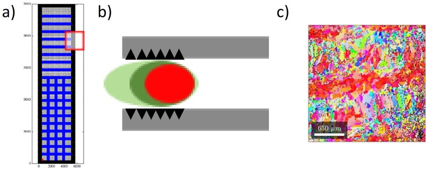
EBM parts utilizing inherent strain method and calibration. The calibration parts shown
in Figure 1 did not show significant deformations, yet a wavy surface profile depending
on the periodic support beneath, which is a phenomenon not encountered in the SLM
process. The preliminary evaluations which will be detailed in the presentation lead to
the conclusion that EBM process simulation at part-scale without taking into account
several mechanisms inherent to the process is not achievable for the moment.
Figure 1: Calibration parts produced along X and Y directions (a) leading to wavy surfaces with
their (b) profiles measured.You can also read