EFFECTS OF EXPOSURE AND AIR ANNEALING ON MOOX THIN FILMS - IRFAN IRFAN YONGLI GAO
←
→
Page content transcription
If your browser does not render page correctly, please read the page content below
Effects of exposure and air annealing on
                 MoOx thin films

                 Irfan Irfan
                 Yongli Gao

Downloaded From: https://www.spiedigitallibrary.org/journals/Journal-of-Photonics-for-Energy on 19 Dec 2021
Terms of Use: https://www.spiedigitallibrary.org/terms-of-use
Effects of exposure and air annealing on MoOx thin films

                                                                     Irfan Irfana and Yongli Gaoa,b
                                 a
                                  University of Rochester, Department of Physics and Astronomy, Rochester, New York 14627
                                                                     ygao@pas.rochester.edu
                                 b
                                  Central South University, Institute for Super Microstructure and Ultrafast Process (ISMUP),
                                                               Changsha, Hunan 410083, China

                                 Abstract. Thermally deposited molybdenum oxide films are investigated with X-ray
                                 photo-emission spectroscopy, ultra-violet photoemission spectroscopy and inverse photoemis-
                                 sion spectroscopy. The Interface between MoOx and copper pthalocynine (CuPc) is studied and
                                 the previously reported device performance improvement is explained, with the help of interface
                                 energy level alignment. The effect of oxygen and air exposure on MoOx films and growth of gap
                                 states with exposures are studied. The surface chemical compositions of MoOx films, of varying
                                 thicknesses from 1 nm to 50 nm, have also been investigated. For all the investigated film
                                 thicknesses, the thermally evaporated films are found to be oxygen deficient. It is believed,
                                 that the oxygen vacancies can be subdued to a great extent by annealing at elevated temperatures.
                                 We annealed the MoOx thin films in air, at 300 °C for 20 h, and investigated the changes induced
                                 by the air annealing. © 2012 Society of Photo-Optical Instrumentation Engineers (SPIE). [DOI: 10.1117/
                                 1.JPE.2.021213]
                                 Keywords: photoemission spectroscopy; molybdenum oxide; organic light emitting diodes;
                                 organic photovoltaic.
                                 Paper 12012SS received Feb. 27, 2012; revised manuscript received May 17, 2012; accepted for
                                 publication Jun. 5, 2012; published online Jun. 27, 2012.

                                 1 Introduction
                                 Organic photovoltaic cells (OPV) have attracted enormous attention due to growing energy
                                 requirements of the world and declining fossil resources.1–6 Recently, a lot of progress has
                                 been made in OPV with the highest power conversion efficiency now being 10.6% for tandem
                                 OPV.7–10 Organic light emitting diode (OLED) has also observed a phenomenal advancement.11–16
                                 Other prominent applications of organic semiconductors include organic thin film transistor
                                 (OTFT), and efficient spin-injection in organic materials.17–20 Many attempts have been
                                 made to improve the charge transport and collection at electrodes. Tokito et al. were the
                                 first to introduce a thin layer of high work function (WF) transition metal oxides between
                                 the conducting indium tin oxide (ITO) and organic semiconductor for efficient OLED devices.21
                                 The importance of the transition metal oxide insertion layer in OPV was successfully demon-
                                 strated by a number of research groups.22–24 The beneficial nature of MoOx has been established,
                                 however, fundamental questions exist in order for comprehensive understanding and controlled
                                 utilization of MoOx insertion layer with reproducible device performance.
                                     One of the fundamental issues is the growth of gap states observed with increasing air
                                 and oxygen exposures on MoOx films.25 The correlation of growth of gap states with the
                                 exposures may provide a better understanding of the role played by MoOx inter-layers in improving
                                 the device performance. Another fundamental issue is oxygen vacancies in thermally evaporated
                                 films from MoO3 powder. The evaporated MoOx films are observed to be strongly n-type due to
                                 the oxygen vacancies (x < 3).26–28 The effect of oxygen vacancies, in the stoichiometric MoO3 film,
                                 is similar to electron doping. The difference of stoichiometric MoO3 versus oxygen deficient
                                 MoOx inter-layers in devices has been recently reported.22 Additionally, it is believed that
                                 the oxygen deficiencies can be suppressed, to a great extent, by annealing MoOx at elevated
                                 temperatures.

                                 0091-3286/2012/$25.00 © 2012 SPIE

                                 Journal of Photonics for Energy                       021213-1                            Vol. 2, 2012

Downloaded From: https://www.spiedigitallibrary.org/journals/Journal-of-Photonics-for-Energy on 19 Dec 2021
Terms of Use: https://www.spiedigitallibrary.org/terms-of-use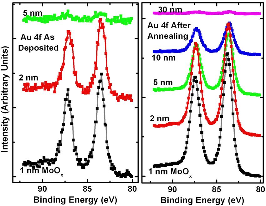
Irfan and Gao: Effects of exposure and air annealing on : : :

                                     In this paper, we report our investigation on effects of exposure and air annealing on the
                                 MoOx thin films. Copper pthalocynine (CuPc)/indium tin oxide (ITO) and CuPc∕MoOx inter-
                                 faces were investigated with ultraviolet photoemission spectroscopy (UPS). We observed the
                                 vacuum level shifts along with changes in the highest occupied molecular orbital (HOMO)
                                 region, with increasing thickness of CuPc film on ITO and MoOx ∕ITO substrates. The mechan-
                                 ism of device improvement is explained with the help of interface energy level alignment. We
                                 also studied the effect of oxygen and air exposures on growth of the gap states with the UPS.
                                 Evolutions of the gap states, with both the exposures, are observed and discussed. The effects of
                                 oxygen and moisture on the MoOx films are observed to progress in two separate stages.
                                     In addition, thermally evaporated MoOx films, of thicknesses 1, 2, 5, 10, 30 and 50 nm, are
                                 investigated with X-ray photoemission spectroscopy (XPS). We measured the oxygen to molyb-
                                 denum ratio and found that the thermally evaporated films are oxygen deficient. In an attempt to
                                 subdue oxygen deficiencies in the MoOx films, we annealed the films, at 300 °C for 20 h, and
                                 measured oxygen to molybdenum values. Our study demonstrates, that contrary to the prevalent
                                 belief, the air annealing is not an efficient process of overcoming the oxygen deficiencies in the
                                 MoOx films.

                                 2 Experiment
                                 The UPS measurements, for the interface formation and the exposure studies, were performed
                                 using an ultrahigh vacuum (UHV) VG ESCA Lab system equipped with a He discharge lamp.
                                 The UHV system consists of a spectrometer chamber interconnected with an evaporation cham-
                                 ber. The base pressure of the spectrometer chamber is typically 8 × 10⁻¹¹ torr. The base pressure
                                 of the evaporation chamber is typically 1 × 10⁻⁶ torr. A precision leak valve is also attached with
                                 the evaporation chamber to leak desired gases in the chamber for exposure studies. The UPS
                                 spectra were recorded by using unfiltered He I (21.22 eV) as the excitation source with the
                                 sample biased at −5.00 V, to observe the low-energy secondary cutoff. The UV light spot
                                 size on the sample is about 1 mm in diameter. The typical instrumental resolution for the
                                 UPS measurements ranges from 0.03 to 0.1 eV, with the photon energy dispersion of less
                                 than 20 meV. Substrates for both studies were cut from a borosilicate glass sheet, from Corning,
                                 Inc. NY, coated with a 250 nm thick conducting ITO film with resistivity of 15Ω per square. The
                                 thicknesses of thermally evaporated films were monitored by quartz crystal microbalance. All
                                 the measurements for the interface studies were performed at room temperature.
                                     XPS spectra were measured with a Surface Science Laboratories’ SSX-100 system, equipped
                                 with a monochromatic Al anode x-ray gun (Kα 1486.6 eV) having resolution limit of 0.5 eV. The
                                 base pressure of the system is 9 × 10 torr. The spot size of the x-ray was selected to be
                                 600 micron in diameter. A substrate, of dimension 11 × 22 mm, for the annealing study was
                                 cut from a gold coated silicon wafer. 10 nm gold was deposited on the substrate with the deposi-
                                 tion rate of ∼1 nm in every 90 s. MoO3 powder was thermally evaporated on the substrate.
                                 A metallic mask with a sharp edge attached to a moveable micrometer, was placed about
                                 ∼2 mm below the substrate to evaporate desired thicknesses of MoOx in a step-wise fashion
                                 on the same substrate. The stepped film eliminates variations associated with the deposition
                                 conditions for films on different substrate. The sample was then transferred in to the UHV cham-
                                 ber for XPS analysis. After the XPS analysis of the thermally evaporated MoOx films of stepped
                                 thicknesses, the sample was taken out and annealed in air at 300 °C for 20 h on a hot plate from
                                 Corning Inc. The temperature was measured with the help of a thermocouple gauge from Fluke.
                                 The sample was then transferred back into the SSX-100 chamber for further XPS analysis.

                                 3 Results and Discussions

                                 3.1 The Effect of MoOx Inter-layer Between CuPc and ITO

                                 3.1.1 CuPc/ITO interface
                                 In Fig. 1, the UPS spectra of CuPc films on ITO are presented as a function of the thickness of the
                                 CuPc films. All the spectra have been normalized to the same height for visual clarity. In Fig. 1(a)

                                 Journal of Photonics for Energy                       021213-2                            Vol. 2, 2012

Downloaded From: https://www.spiedigitallibrary.org/journals/Journal-of-Photonics-for-Energy on 19 Dec 2021
Terms of Use: https://www.spiedigitallibrary.org/terms-of-use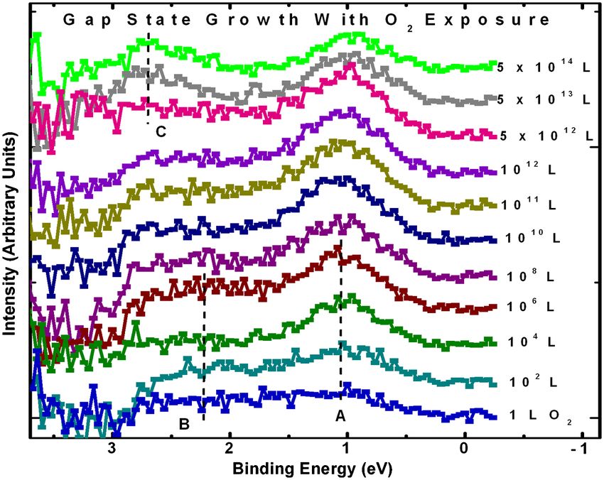
Irfan and Gao: Effects of exposure and air annealing on : : :

                                 Fig. 1 The UPS spectra of CuPc on ITO as a function of CuPc thickness. The cut-off and the
                                 HOMO regions are presented in Fig. 1(a), and 1(b), respectively.

                                 and 1(b), the cut-off and the HOMO regions are presented, respectively. The cut-off binding
                                 energy (BE) of the ITO substrate was measured to be 16.57 eV, which corresponds to a surface
                                 work function of 4.65 eV, obtained by subtracting the cut-off BE from the photon energy of the
                                 excitation source (21.22 eV). With increasing thickness of the CuPc film, we observed cut-off
                                 shift towards the lower WF (or higher cut-off BE) values. The shift saturated around 32 Å CuPc
                                 thickness. From Fig. 1(b), the HOMO onset for 8 Å CuPc film was measured at 0.31 eV. With
                                 further increase in the CuPc thickness, the occupied level peaks remained more or less
                                 unchanged on the HOMO peaks, as illustrated by the dashed line in the figure.

                                 3.1.2 CuPc∕MoOx interface
                                 In Fig. 2, the UPS data for the cut-off and the HOMO regions are plotted in Fig. 2(a) and 2(b),
                                 respectively. The ITO WF was measured to be 4.59 eV and, with the deposition of a 100 Å MoOx
                                 film, the WF was measured to be 6.82 eV. With the deposition of CuPc on MoOx ∕ITO, the WF
                                 first decreased rapidly, then the shift in WF became more gradual. In Fig. 2(b), the valence band
                                 peak of MoOx was observed at ∼3.8 eV. The MoOx peak shows a gradual shift towards the
                                 higher BE with increasing thickness of CuPc. This shift was measured to be ∼0.2 eV up to

                                 Fig. 2 The UPS spectra of CuPc on MoOx ∕ITO as a function of CuPc thickness. The cut-off and
                                 the HOMO regions are presented in Fig. 1(a) and 1(b), respectively.

                                 Journal of Photonics for Energy                       021213-3                             Vol. 2, 2012

Downloaded From: https://www.spiedigitallibrary.org/journals/Journal-of-Photonics-for-Energy on 19 Dec 2021
Terms of Use: https://www.spiedigitallibrary.org/terms-of-use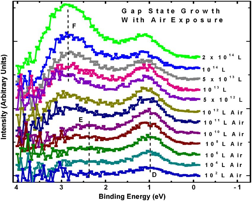
Irfan and Gao: Effects of exposure and air annealing on : : :

                                 8 Å of CuPc deposition. With further CuPc deposition, all the occupied level peaks
                                 were observed to be continuously shifting towards the higher BE. The HOMO onset
                                 BE for 8 Å, 64 Å, and 200 Å thick CuPc films were measured to be 0.21, 0.36, and
                                 0.53 eV, respectively.

                                 3.1.3 Energy level alignment
                                 The energy level alignment diagrams for the CuPc/ITO and the CuPc∕MoOx interfaces are pre-
                                 sented in Fig. 3(a) and 3(b), respectively. The band gap of 3.2 eV for MoOx and 1.7 eV for CuPc
                                 hasbeen reported in our earlier works.26–30 In Fig. 3(a), the ITO WF was measured to be 4.65 eV.
                                 At the CuPc/ITO interface, we observed an interface dipole of 0.33 eV, due to transfer of holes
                                 from ITO to the CuPc side. After the formation of the interface dipole, a near flat band situation
                                 was observed. The initial hole injection barrier was measured to be 0.31 eV, with the ionization
                                 potential (IP) of 4.65 eV. In Fig. 3(b), the ITO WF was measured to be 4.59 eV, which became
                                 6.82 eV with the deposition of 100 Å MoOx . With the deposition of CuPc on MoOx ∕ITO, the
                                 energy levels of MoOx shift towards the higher BE and a large dipole moment at the interface is
                                 observed, due to the rapid transfer of holes from MoOx side to the organic side. The conservative
                                 estimate of the shift is 0.2 eV in the MoOx energy levels towards the higher BE. The estimate is
                                 made from the shift of MoOx valence band peak towards the higher BE with the deposition of
                                 CuPc, as depicted in Fig. 2(b). The large interface dipole of 2.97 eV is observed at the interface.
                                 The initial hole injection barrier is observed to be 0.21 eV. With further depsition of CuPc, the
                                 energy levels gradually relax back to their normal values, thus, creating a band bending like
                                 region in the organic side. At the thickness of 200 Å CuPc, the HOMO onset value was measured
                                 to be 0.53 eV.
                                     Kim et al. have reported 30 percent improvement in the fill factor (FF) and 37 percent
                                 improvement in the overall power conversion efficiency, with a 100 Å MoOx inter-layer between
                                 ITO anode and a CuPc layer.24 We assign the improvement to the lower hole injection barrier at
                                 the CuPc∕MoOx interface and the presence of a drift electric field. There are two possible
                                 improvement mechanisms in the presence of the drift electric field. The first is that the drift
                                 field is a steering field which is helpful for easier extraction of holes at the anode.24 The second
                                 is that the field facilitates the absorption of photons incident on the material through transparent
                                 anode side, which is supported by the reported improved absorption with MoOx inter-layer.31

                                 3.2 Oxygen and Air Exposure to Molybdenum Oxide Thin Films

                                 3.2.1 Evolution of gap states with oxygen exposure
                                 In our earlier report, we have demonstrated the effect of oxygen exposure on valence band region
                                 and WF of MoOx thin films.25 High WF (∼6.8 eV), of thermally evaporated MoOx films,
                                 decreases sharply with oxygen exposure before reaching a saturation (>5.8 eV). In Fig. 4,
                                 the evolution of gap states in the valence band region is presented with increasing oxygen

                                 Fig. 3 The energy level alignment diagrams for, (a) CuPc on ITO, and (b) CuPc on MoOx ∕ITO
                                 interfaces.

                                 Journal of Photonics for Energy                       021213-4                            Vol. 2, 2012

Downloaded From: https://www.spiedigitallibrary.org/journals/Journal-of-Photonics-for-Energy on 19 Dec 2021
Terms of Use: https://www.spiedigitallibrary.org/terms-of-use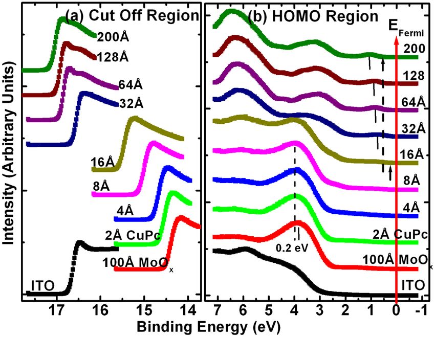
Irfan and Gao: Effects of exposure and air annealing on : : :

                                 exposure on a 50 Å MoOx film. The spectra of gap states are obtained by subtracting valence
                                 region spectrum of evaporated MoOx film from the background of the valence band region of
                                 individual exposed spectrum. Before background subtraction, the dominant oxygen 2p peak
                                 intensities were normalized and peak position of the evaporated spectrum was shifted to
                                 match the peak positions of each of the exposed spectrum. In the figure, we observe the growth
                                 of a gap state at 5.4eV). In Fig. 5,
                                 the growth of gap states in the valence band region is presented with increasing air exposure on a
                                 50 Å MoOx film. The presented spectra are obtained by subtracting valence region spectrum of
                                 thermally evaporated MoOx film from a background, as described in Sec. 3.2.1. We observed
                                 the growth of a gap state around 1.0 eV, marked as ‘D’ in the figure, which is similar to the gap
                                 state ‘A’ in Sec. 3.2.1. Initially, the intensity of the state ‘D’ increases sharply with air
                                 exposures, then it saturates around 108 L exposure. The gap state ‘D’ is dominant until
                                 1012 L exposure. Another gap state ‘E’, at ∼2.3 eV, is also observed which is similar to the
                                 state ‘B’ of the previous section. Initially, the intensity of the state ‘E’ is low. The gap state,
                                 marked as ‘F’, develops at a mature exposure stage around ∼2.9 eV. At the final air exposure,
                                 the intensity of the ‘F’ state is dominant in the spectrum. In the next section, we will compare the
                                 evolutions of gap states with the exposures.

                                                        Fig. 4 The evolution of gap states with oxygen exposure.

                                 Journal of Photonics for Energy                       021213-5                             Vol. 2, 2012

Downloaded From: https://www.spiedigitallibrary.org/journals/Journal-of-Photonics-for-Energy on 19 Dec 2021
Terms of Use: https://www.spiedigitallibrary.org/terms-of-use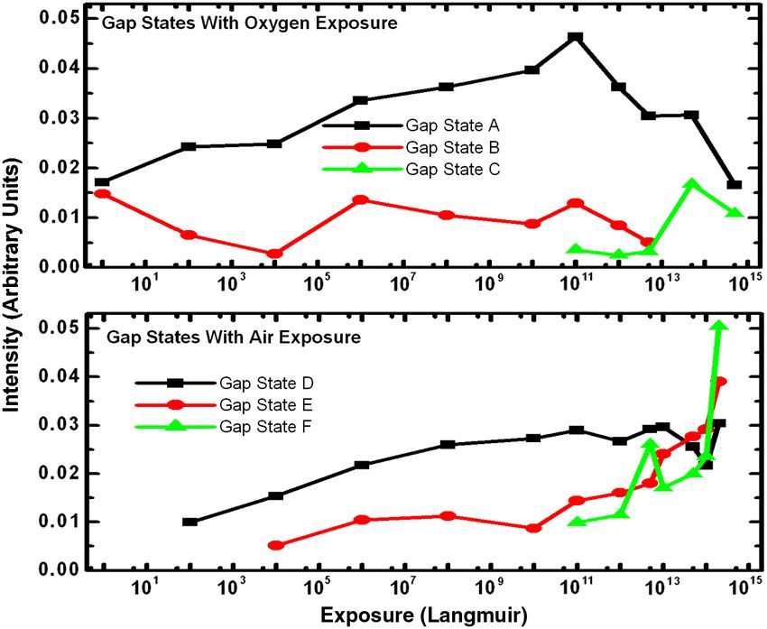
Irfan and Gao: Effects of exposure and air annealing on : : :

                                                           Fig. 5 The evolution of gap states with air exposure.

                                 3.2.3 Comparison of growths of gap states
                                 In Fig. 6, relative intensities of the gap states are presented as a function of the exposures. The
                                 intensities of the gap states with the oxygen exposures are presented in Fig. 6(a), and with the air
                                 exposures are presented in Fig. 6(b). Comparing the evolution of states ‘A’ and ‘D’, both the gap
                                 states can be assigned to the effect of oxygen on the MoOx films. While comparing the evolution
                                 of states ‘C’ and ‘F’, the origin of these states can be attributed to the effect of moisture on the
                                 MoOx films. Earlier, we have reported that the WF reduction in exposed MoOx films is a two
                                 stage process. The first stage of reduction is caused by adsorption of oxygen on the MoOx
                                 films.25 This stage reduces the WF from 6.8 to ∼5.8 eV. The second stage of WF drop is caused

                                                 Fig. 6 The comparison of gap states with air and oxygen exposures.

                                 Journal of Photonics for Energy                       021213-6                            Vol. 2, 2012

Downloaded From: https://www.spiedigitallibrary.org/journals/Journal-of-Photonics-for-Energy on 19 Dec 2021
Terms of Use: https://www.spiedigitallibrary.org/terms-of-use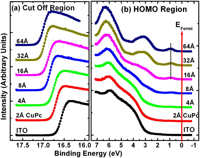
Irfan and Gao: Effects of exposure and air annealing on : : :
by the adsorption of moisture on the MoOx films. It is interesting to note, that a gap state similar
to the ‘A’ and the ‘D’ states, also around 1 eV, has been reported earlier by Nakayama et al. on the
initial deposition of MoOx on poly(dioctylfluorine-alt-benzothiadiazole) (F8BT).28 Therefore, it
can be concluded that the first stage WF drop, caused by oxygen exposure, must be related to the
charge transfer between adsorbed oxygen and the surface of MoOx film.
3.2.4 Correlation of gap states with device performance and work function
In one of our earlier reports, we have demonstrated a substantial degradation in the device per-
formance with 15 min (∼7 × 10¹¹ L) of air exposure of the MoOx film.25 The exposures over
1011 L also mark the appearance of the gap state ‘F’ in Fig. 6. Since the growth of the gap state
‘F’ is caused by moisture, as discussed earlier, we attribute the major degradation in the device to
the gap state ‘F’. In another report, a similar degradation was observed in the OPV performance
by 30 min (∼1.4 × 10¹² L) of air exposure.33 It should be noted, that both Nakayama et al.28 and
Maria et al have attributed the improvement of device performance to the presence of the gap
state similar to the D state around 1 eV.29 In our understanding, the WF reduction, from high
6.8 eV to moderate (∼5.8 eV), is coupled with the growth of gap state ‘D’ (or ‘A’ for O2 expo-
sure) and may not be significantly deleterious to devices since the reduced WF is still higher than
the ionization potential of most of the organic semiconductors. The appearance of the gap state
‘F’, which further reduces the WF from ∼5.8 to 5.4 eV, is probably the most harmful to devices.
Meyer et. al., have also reported no significant effect on the device performance with an air
exposure of 3 min (1011 L), probably just before the appearance of the gap state F.34 However,
at present, an exact correlation of gap states is not well established and further investigations are
required for this to be accomplished.
3.3 Effect of Annealing on Molybdenum Oxide Thin Films
In the Sec. 3.1, we reported the beneficial nature of an insertion layer of MoOx film which is in
agreement with many earlier reports.21–24 In the Sec. 3.2, we established that the performance can
be substantially affected by high exposures of MoOx films. In this section, we will explore
another fundamental issue related with the stoichiometry of MoOx films. The deposition of
MoOx insertion layer is mostly achieved with thermal evaporation of MoO3 powder. Thermally
deposited MoOx films are known to be oxygen deficient (x < 3).35,36 The oxygen deficiencies are
also reported to cause gap states, at ∼1.1 eV and 2.3 eV, which can affect the device perfor-
mance.29 Some reports suggest that annealing can replenish oxygen deficiencies.37,38 In this sec-
tion, we will investigate the stoichimetry of thermally evaporated MoOx films and explore the
effect of air annealing on the stoichiometry.
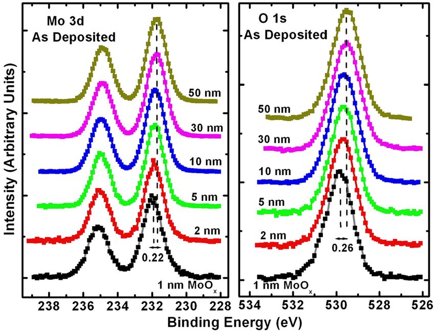
3.3.1 Thermally evaporated MoOx film
In Fig. 7, the XPS data of Mo 3d5∕2 and O 1s core levels, for 1, 2, 5, 10, 30, and 50 nm thick-
nesses, are plotted. All the spectra have been normalized to the same height for visual clarity. In
Fig. 7(a), the 3d core level of molybdenum consists of two spin orbit interaction split peak, 3d5∕2
and 3d5∕2 with the peak separation of 3.15 eV and the intensity ratio of 3∶2. The 3d5∕2 peak, for
1 nm thickness, was observed at the binding energy (BE) of 231.97 eV. With the increasing
thickness of MoOx film, the 3d peaks kept gradually shifting towards the lower BE before reach-
ing a saturation at around 30 nm. The overall peak shift, measured in the range of investigation,
was 0.23 eV. The full width at half the maximum height (FWHM) of 3d peaks were measured to
be ∼1.35 eV. In Fig. 7(b), the oxygen 1s core levels, with a dominant peak at the BE of
529.81 eV and a very low intensity peak around ∼530.90 eV, are observed for 1 nm thickness.
With increasing thickness of the MoOx film, the dominant oxygen peak kept gradually shifting
towards the lower BE with the saturation setting in around 30 nm. The overall peak shift mea-
sured from 1 to 50 nm MoOx film thickness was 0.26 eV. The FWHM for the dominant peak was
∼1.4 eV up to 5 nm, which increased to ∼1.55 eV for thicker films. A shift of ∼0.2 eV in the
MoOx work function (WF) and the valence band peak towards the lower BE has been reported
with increasing film thickness from 2 to 30 nm on indium tin oxide (ITO) substrate (19). The
Journal of Photonics for Energy 021213-7 Vol. 2, 2012
Downloaded From: https://www.spiedigitallibrary.org/journals/Journal-of-Photonics-for-Energy on 19 Dec 2021
Terms of Use: https://www.spiedigitallibrary.org/terms-of-use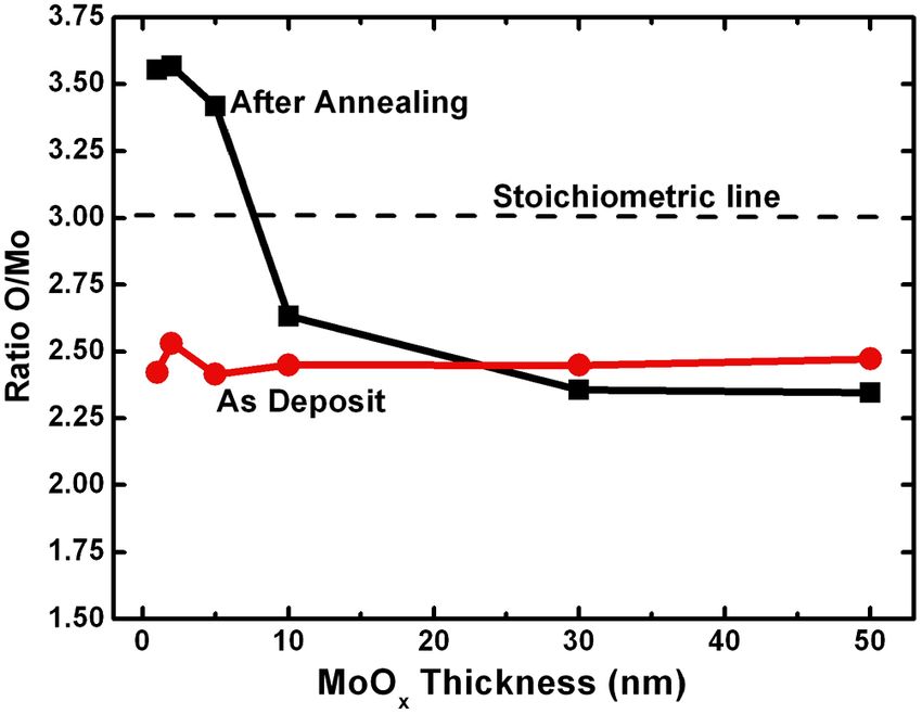
Irfan and Gao: Effects of exposure and air annealing on : : :

                                 Fig. 7 XPS spectra of (a) Mo 3d, and (b) O 1s core levels as a function of increasing MoOx film
                                 thicknesses.

                                 shift of core levels, observed in the present case, are consistent with the WF shift which further
                                 suggests that the shift extend to deep core levels rather than just shallow lying valence band and
                                 vacuum level. We also observed Au 4f peaks, originating from substrate, for thin MoOx deposi-
                                 tions up to 5 nmwhich will be discussed later in this work.

                                 3.3.2 Annealing of MoOx films
                                 In Fig. 8, the XPS data of Mo 3d and O 1s core levels are plotted for 1, 2, 5, 10, 30, 50 nm
                                 thicknesses, after annealing in air at 300 °C for 20 h. All the spectra have been normalized to the
                                 same height for visual clarity. In Fig. 8(a), the 3d5∕2 peak for 1 nm thickness was observed at the
                                 BE of 231.13 eV. With increasing thickness of MoOx film, a complex peak shift pattern was
                                 observed. We also observed diffusion of gold from substrate towards the top surface through
                                 MoOx film due to annealing for long time at high temperature. The complex peak shift pattern is
                                 originated due to diffusion of gold which will be discussed in the next section. The FWHM of 3d
                                 peaks was measured to be ∼1.35 eV. In Fig. 8(b), the oxygen 1s core level, with a dominant peak

                                 Fig. 8 XPS spectra of (a) Mo 3d, and (b) O 1s core levels after the annealing, as a function of
                                 increasing MoOx film thicknesses.

                                 Journal of Photonics for Energy                       021213-8                            Vol. 2, 2012

Downloaded From: https://www.spiedigitallibrary.org/journals/Journal-of-Photonics-for-Energy on 19 Dec 2021
Terms of Use: https://www.spiedigitallibrary.org/terms-of-use
Irfan and Gao: Effects of exposure and air annealing on : : :
at the BE of 530.08 eV and a low intensity peak around ∼531.44 eV, was observed for 1 nm
thickness. The complex peak shift, after annealing, was also present in O 1s core levels with
increasing thickness of the MoOx film.
3.3.3 Comparison of oxygen to molybdenum ratio
XPS spectra of Au 4f peaks for as deposited and after air annealing are presented in Fig. 9 in
order to understand the changes brought in by the annealing. In Fig. 9(a), the 4f core levels of
gold consist of two spin orbit interaction split peaks 4f7∕2 and 4f5∕2 with the peak separation of
4.3 eV and the intensity ratio of 4∶3. The intensity of 4f peaks kept continuously decreasing and,
at 5 nm thickness of MoOx layer, the intensity of this peak is insignificant. After annealing, the
intensity of Au 4f peaks became more than 10 times higher for 1 nm MoOx thickness, which
strongly indicates the diffusion of Au from substrate towards the top surface. With increasing
MoOx thickness, the intensity of Au 4f peaks kept continuously decreasing. The intensity of Au
4f peaks at 10 nm MoOx thickness, after annealing, is about four times higher that of 1 nm MoOx
for as deposited film. At the 30 nm film thickness, the intensity of Au 4f peaks are low, indicating
that the gold diffusion does not significantly affect the surface for such thicknesses. As men-
tioned earlier in the annealing section, the complex peak shift in the Mo 3d and the O 1s peaks
observed after the annealing is most likely originated due to the diffusion of gold.
In Fig. 10, the intensity ratio of oxygen to molybdenum are plotted for 1, 2, 5, 10, 30, and
50 nm thicknesses of MoOx films before and after the annealing. As obvious from figure, we
measured the oxygen to molybdenum ratio about 2.45, with small variation, for deposited film.
After annealing, the ratio was initially higher than the stoichiometric value of 3.0 which quickly
drops and saturates around ∼2.35. Higher value of oxygen to molybdenum ratio, up to 10 nm, is
due to higher oxygen content at these thicknesses. As discussed in the previous figure, the
annealing of MoOx thin film with gold substrate causes diffusion of gold atoms towards the
surface and substantially enhances the contribution of gold in the surface chemical composition.
The contribution becomes insignificant for the 30 nm thick film. Chemisorption of oxygen mole-
cules on gold at high temperature has been reported earlier.39 Therefore, the enhancement of
oxygen intensity for the air annealed MoOx film at the early stage is due to the chemisorption
of oxygen on the diffused gold atoms. Since we do not have significant diffusion of gold on
surface (or sub surface) for thicknesses ≥30 nm, the contribution from the chemisorbed oxygen
on gold is insignificant. The measured oxygen to molybdenum ratio, in the saturated thickness
region, is slightly less (∼2.35) for the annealed MoOx film than the as deposit film (∼2.45).
Thus, the current investigation establishes that the air annealing does not significantly suppress
oxygen vacancies present in the thermally evaporated MoOx films.
Fig. 9 XPS spectra of Au 4f for (a) a deposit, and (b) after annealing. After annealing intensity of
Au 4f peaks increased, indicating diffusion of gold from substrate towards the top surface.
Journal of Photonics for Energy 021213-9 Vol. 2, 2012
Downloaded From: https://www.spiedigitallibrary.org/journals/Journal-of-Photonics-for-Energy on 19 Dec 2021
Terms of Use: https://www.spiedigitallibrary.org/terms-of-useIrfan and Gao: Effects of exposure and air annealing on : : :
Fig. 10 Oxygen to molybdenum ratio for as deposited and air annealed film with increasing thick-
ness of MoOx film. High ratio after the annealing for thin MoOx film is due to the absorption of
oxygen and moisture on diffused gold atoms.
4 Conclusions
In conclusion, we have investigated the effect of MoOx inter-layer between ITO anode and CuPc.
In the presence of MoOx , energy levels of organic side are strongly pulled upwards due to high
workfunction of MoOx films, therefore, reducing the hole injection barrier at the interface. The
energy levels of organic side gradually relax, therefore, creating a band bending like situatio,
which creates a drift electric field. The reduced hole injection barrier and the drift electric field is
beneficial for the performance of OLED and OPV devices. Additionally, we have investigated
thermally evaporated 1, 2, 5, 10, 30, and 50 nm thick MoOx films and measured oxygen to
molybdenum ratio for these thicknesses. All the films were found to be oxygen deficient
(x < 3). We performed air annealing of MoOx films, in air at 300 °C for 20 h, and established
that the annealing does not assist in reducing the oxygen vacancies.
Acknowledgments
The authors would like to acknowledge the support of the National Science Foundation Grant
No. DMR-1006098.
References
1. C. W. Tang, “Two‐layer organic photovoltaic cell,” Appl. Phys. Lett. 48(2), 183–185 (1986),
http://dx.doi.org/10.1063/1.96937.
2. G. Yu et al., “Polymer photovoltaic cells: enhanced efficiencies via a network of internal
donor-acceptor heterojunctions,” Science 270(5423), 1789–1791 (1995), http://dx.doi.org/
10.1126/science.270.5243.1789.
3. P. Peumans and S. R. Forrest, “Very-high-efficiency double-heterostructure copper phtha-
locyanine/C-60 photovoltaic cells,” Appl. Phys. Lett. 79(1), 126–128 (2001), http://dx.doi
.org/10.1063/1.1384001.
4. J. Xue et al., “4.2% efficient organic photovoltaic cells with low series resistances,” Appl.
Phys. Lett. 84(16), 3013–3015 (2004), http://dx.doi.org/10.1063/1.1713036.
5. G. Li et al., “High-efficiency solution processable polymer photovoltaic cells by self-
organization of polymer blends,” Nat. Mater. 4(11), 864–868 (2005), http://dx.doi.org/
10.1038/nmat1500.
6. C. J. Brabec, “Organic photovoltaics: technology and market,” Sol. Energy Mater. Sol. Cells
83(2–3), 273–292 (2004), http://dx.doi.org/10.1016/j.solmat.2004.02.030
Journal of Photonics for Energy 021213-10 Vol. 2, 2012
Downloaded From: https://www.spiedigitallibrary.org/journals/Journal-of-Photonics-for-Energy on 19 Dec 2021
Terms of Use: https://www.spiedigitallibrary.org/terms-of-useIrfan and Gao: Effects of exposure and air annealing on : : :
7. Y. Sun et al., “Solution-processed small-molecule solar cells with 6.7% efficiency,” Nat.
Mater. 11(1), 44–48 (2012), http://dx.doi.org/10.1038/nmat3160.
8. C. E. Small and F. So, “High-efficiency inverted dithienogermole-thienopyrrolodione-based
polymer solar cells,” Nat. Photonics 6(2), 115–120 (2012), http://dx.doi.org/10.1038/
nphoton.2011.317.
9. G. Li, R. Zhu, and Y. Yang, “Polymer solar cells,” Nat. Photonics 6(3), 153–161 (2012),
http://dx.doi.org/10.1038/nphoton.2012.11.
10. National Renewable Energy Laboratory (NREL) www.nrel.gov/ncpv/images/
efficiency_chart.jpg.
11. C. W. Tang and S. A. Vanslyke, “Organic electroluminescent diodes,” Appl. Phys. Lett. 51
(12), 913–915 (1987), http://dx.doi.org/10.1063/1.98799.
12. R. H. Friend et al., “Electroluminescence in conjugated polymers,” Nature 397(67), 121–
128 (1999), http://dx.doi.org/10.1038/16393.
13. S. J. Su et al., “Highly efficient organic blue-and white-light-emitting devices having a car-
rier- and exciton-confining structure for reduced efficiency roll-off,” Adv. Mater. 20(21),
4189–4194 (2008), http://dx.doi.org/10.1002/adma.200801375.
14. M. G. Helander et al., “Chlorinated indium tin oxide electrodes with high work function for
organic device compatibility,” Science 332(6032), 944–947 (2011), http://dx.doi.org/10
.1126/science.1202992.
15. Z. B. Wang et al., “Unlocking the full potential of organic light-emitting diodes on flexible
plastic,” Nat. Photonics 5(12), 753–757 (2011), http://dx.doi.org/10.1038/nphoton.2011.259.
16. T. H. Han et al., “Extremely efficient flexible organic light-emitting diodes with modified
graphene anode,” Nat. Photonics 6, 105–110 (2012), http://dx.doi.org/10.1038/nphoton
.2011.318.
17. G. Horowitz, “Organic field-effect transistors,” Adv. Mater. 10(5), 365–377(1998), http://dx
.doi.org/10.1002/(ISSN)1521-4095.
18. C. D. Dimitrakopoulos and D. J. Mascaro, “Organic thin-film transistors: A review of recent
advances,” IBM J.Res. Dev. 45(1), 11–27 (2001), http://dx.doi.org/10.1147/rd.451.0011.
19. Z. H. Xiong et al., “Giant magnetoresistance in organic spin-valves,” Nature 427(6977),
821–824 (2004), http://dx.doi.org/10.1038/nature02325.
20. M. Cinchetti et al., “Determination of spin injection and transport in a ferromagnet/organic
semiconductor heterojunction by two-photon photoemission,” Nat. Mater. 8(2), 115–119
(2009), http://dx.doi.org/10.1038/nmat2334.
21. S. Tokito, K. Noda, and Y. Taga, “Metal oxides as a hole-injecting layer for an organic
electroluminescent device,” J. Phys. D-Appl. Phys. 29(11), 2750–2753 (1996), http://dx
.doi.org/10.1088/0022-3727/29/11/004.
22. V. Shrotriya et al., “Transition metal oxides as the buffer layer for polymer photovoltaic
cells,” Appl. Phys. Lett. 88(7), 073508–073510 (2006), http://dx.doi.org/10.1063/1
.2174093.
23. M. D. Irwin et al., “p-Type semiconducting nickel oxide as an efficiency-enhancing anode
interfacial layer in polymer bulk-heterojunction solar cells,” PNAS 105(8), 2783–2787
(2008), http://dx.doi.org/10.1073/pnas.0711990105.
24. D. Y. Kim et al., “The effect of molybdenum oxide interlayer on organic photovoltaic cells,”
Appl. Phys. Lett. 95(9), 093304–093306 (2009), http://dx.doi.org/10.1063/1.3220064.
25. Irfan H. Ding et al., “Energy level evolution of air and oxygen exposed molybdenum tri-
oxide films,” Appl. Phys. Lett. 96(24), 243307–243310 (2010), http://dx.doi.org/10.1063/1
.3454779.
26. Irfan H. Ding et al., “Energy level evolution of molybdenum trioxide interlayer between
indium tin oxide and organic semiconductor,” Appl. Phys. Lett. 96(7), 073304–073306
(2010), http://dx.doi.org/10.1063/1.3309600.
27. M. Kroger et al., “P-type doping of organic wide band gap materials by transition metal
oxides: A case-study on Molybdenum trioxide,” Org. Electron 10(5), 932–938 (2009),
http://dx.doi.org/10.1016/j.orgel.2009.05.007.
28. Y. Nakayama et al., “Origins of improved hole-injection efficiency by the deposition of
MoO(3) on the polymeric semiconductor poly (dioctylfluorene-alt-benzothiadiazole),”
Adv. Funct. Mater. 19(23), 3746–3752 (2009), http://dx.doi.org/10.1002/adfm.v19:23.
Journal of Photonics for Energy 021213-11 Vol. 2, 2012
Downloaded From: https://www.spiedigitallibrary.org/journals/Journal-of-Photonics-for-Energy on 19 Dec 2021
Terms of Use: https://www.spiedigitallibrary.org/terms-of-useIrfan and Gao: Effects of exposure and air annealing on : : :
29. V. Maria et al., “Reduced molybdenum oxide as an efficient electron injection layer in poly-
mer light-emitting diodes,” Appl. Phys. Lett. 98(12), 123301 (2010),.http://dx.doi.org/10
.1063/1.3557502.
30. L. Yan et al., “Direct observation of fermi-level pinning in Cs-doped CuPc film,” Appl.
Phys. Lett. 79(25), 4148–4150 (2001), http://dx.doi.org/10.1063/1.1426260.
31. D. Y. Kim, G. Sarasqueta, and Franky So, “SnPc: C(60) bulk heterojunction organic photo-
voltaic cells with MoO(3) interlayer,” Sol. Ener. Mat. Sol. Cells 93(8), 1452–1456 (2009),
http://dx.doi.org/10.1016/j.solmat.2009.03.011.
32. Irfan M. Zhang et al., “Strong interface p-doping and band bending in C(60) on MoO(x),”
Org. Electron. 12(9), 1588–1593 (2011), http://dx.doi.org/10.1016/j.orgel.2011.06.007.
33. M. Zhang et al., “Organic Schottky barrier photovoltaic cells based on MoO(x)/C(60),”
Appl. Phys. Lett. 96(18), 183301–183303 (2010), http://dx.doi.org/10.1063/1.3415497.
34. J. Meyer et al., “Effect of contamination on the electronic structure and hole-injection prop-
erties of MoO3/organic semiconductor interfaces,” Appl. Phys. Lett. 96(13), 133308–
133310 (2010), http://dx.doi.org/10.1063/1.3374333.
35. M. Anwar and C. A. Hogarth, “The correlation of various properties of thin-films of moo3
and of the mixed-oxide systems moo3-in2o3 and moo3-sio,” Mater. J. Sci. 25(11), 4918–
4928 (1990), http://dx.doi.org/10.1007/BF01129962.
36. T. He and J. Yao, “Photochromism of molybdenum oxide,” Photochem. J. Photobiol. C
4(2), 125–143 (2003), http://dx.doi.org/10.1016/S1389-5567(03)00025-X.
37. R. S. Patil, M. D. Uplane, and P. S. Patil, “Electrosynthesis of electrochromic molybdenum
oxide thin films with rod-like features,” Int. J. Electrochem. Sci. 3(3), 259–265 (2008).
38. V. Bhosle, A. Tiwari, and J. Narayan, “Epitaxial growth and properties of MoOx(2 < x <
2.75) films,” J. Appl. Phys. 97(8), 083539–083543 (2005), http://dx.doi.org/10.1063/1
.1868852.
39. M. A. Chesters and G. A. Somerjai, “The chemisorption of oxygen, water and selected
hydrocarbons on the (111) and stepped gold surfaces,” Surf. Sci. 52(1), 21–28 (1975),
http://dx.doi.org/10.1016/0039-6028(75)90004-7.
Irfan Irfan is a PhD candidate in the Department of Physics and Astronomy at the University
of Rochester under the supervision of Professor Yongli Gao. In 2004, he received a BS from
the University of Lucknow. He received his MS in physics in 2006 from S. N. Bose National
Institute for basic Sciences, Kolkata, India. He joined the University of Rochester in 2007 and
is currently studying electronic structure and energy-level alignment at metallorganic
semiconductor, metal/oxide/organic semiconductor interfaces. These studies are helpful in
understanding and predicting device performances of OLED and OPV cell. His
current work focuses on the role of molybdenum tri-oxide insertion layers at the anode
of organic semiconductor devices.
Yongli Gao received his BS in physics from Central-South Institute of Mining and
Metallurgy, China in 1981, and PhD in physics from Purdue University in 1986 under the
guidance of Professor Ron Reifenberger. From 1986 to 1988, he was a postdoctoral fellow
with Professor John Weaver at University of Minnesota. He joined the faculty of the University
of Rochester in 1988 and was promoted to associate professor and full professor in physics in
1994 and 1999, respectively. He has published over 200 papers on interface formation in organic
semiconductors, ultrafast electronic dynamics in metals, semiconductors, and quantum wells,
surface stability and interface formation of high Tc superconductors, low-temperature Schottky
barrier formation and dielectric layer formation on III–V semiconductors, surface melting, and
mechanisms of x-ray photoelectron and Auger electron diffraction.
Journal of Photonics for Energy 021213-12 Vol. 2, 2012
Downloaded From: https://www.spiedigitallibrary.org/journals/Journal-of-Photonics-for-Energy on 19 Dec 2021
Terms of Use: https://www.spiedigitallibrary.org/terms-of-useYou can also read