Enabling cost-competitive mass production of micro-LED displays
←
→
Page content transcription
If your browser does not render page correctly, please read the page content below
48 Technology focus: LEDs

   Enabling cost-competitive
   mass production of
   micro-LED displays
   A
         LLOS Semiconductors explains how GaN-based                      improvements in conventional LCD and OLED displays
         micro-LEDs grown by MOCVD on 200mm or                           — skeptical observers asked two questions: Firstly, can
         300mm silicon wafers offers huge cost and yield                 micro-LED-based products really deliver broad and
   advantages compared with GaN-on-sapphire.                             decisive customer benefits or will they be limited to some
                                                                         niche applications? And secondly, can such products
   The challenge to bring micro-LEDs into                                achieve the yield and cost levels that actually allow
   mass production                                                       profitable mass production anytime soon?
   The quest to use micron-sized light-emitting diodes                     Regarding the first question, companies like Samsung,
   (micro-LED) for the next generation of high-performance               Plessey, PlayNitride, X-Celeprint, Rohinni and many
   displays has led to dramatic progress in recent years.                others have answered with a wide range of impressive
   After the first demonstrators of these novel displays in              micro-LED-based display prototypes and first flagship
   2012, the potentially huge advantages of this technology              products. As Eric Virey of market research company
   for end-product design, shape and performance have                    Yole Développement observes: “We see two hot
   been recognized quickly. Compared with conventional                   candidates for early micro-LED adaptation: Very small
   liquid-crystal displays (LCDs) and organic light-emitting             and very big displays. Very small displays (e.g. for AR
   diode (OLED)-based displays, micro-LED displays                       glasses) benefit from the tiny micro-LED dimensions and
   promise higher brightness including readability in                    corresponding high pixel density and they even offer
   sunlight, better contrast, higher speed, wider viewing                unmatched high brightness. This is enabling a truly new
   angles as well as improved lifetime, ruggedness and                   consumer experience. In contrast, very large displays
   environmental stability. More importantly, micro-LED                  have the benefit of micro-LED displays’ unique cost
   displays are extremely energy-efficient, which will                   structure. While the cost of conventional TVs depends
   boost the battery run-time – essential to mobile appli-               largely on the display area, the cost of micro-LED
   cations like smart watches, augmented reality (AR)                    displays is driven mainly by the number of pixels and
   glasses or smartphones – and curb the ever increasing                 thus micro-LED chips. This means that the cost for a
   electricity consumption of displays in general.                       4K display with a size of 100-inches can be almost the
     In a micro-LED display each pixel is made of three                  same as for a 73-inch display. These unique economics
   tiny LEDs emitting red, green and blue (RGB) light.                   can drive down the cost of large high-quality displays
   Despite being as small as 2µm in edge length compared                 and thus generate a huge new market demand.”
   with 60µm diameter for a human hair or 300µm for a                    The success of such products would provide an initial
   typical conventional LED, these LEDs are still sufficiently           critical volume to reduce the cost of micro-LED dis-
   bright. This means that high-resolution displays can be               plays and mature the technology for other products
   transparent and thus seamlessly integrated even into                  like smartphones or automotive applications.
   glasses or contact lenses. At the same time there is                    This makes it even more urgent to address the
   plenty of space between the pixels that product                       second question of how to improve the yield and cost
   designers want to utilize for example for sensors or                  levels to enable mass production. Although developers
   solar cells. This will change the way we build and use                increasingly find solutions for individual production
   displays: Virtually any surface can become a display                  challenges like the processing accuracy of tiny micro-
   while any ‘display’ can also have a multitude of func-                LED chips or for assembling them using so-called
   tionalities. The first demonstrators already show                     mass-transfer technologies, the end-to-end yield of
   micro-LED displays integrated into windows of cars or                 the entire manufacturing chain remains insufficient.
   buildings, furniture, textiles or even wallpaper.                     The biggest hurdle for manufacturability is the sheer
     Realizing this disruptive potential, huge corporations              amount of chips of constant quality needed for a single
   like Sony and Apple (as well as many start-ups) began                 display: A 4K display consists of over 8 million pixels,
   to invest early in micro-LED development. However,                    and thus a total of almost 25 million so-called sub-pixels
   given the technical challenges — but also the constant                (consisting of micro-LED chips for red, green and blue

   semiconductor TODAY Compounds&AdvancedSilicon • Vol. 15 • Issue 3 • April/May 2020                  www.semiconductor-today.com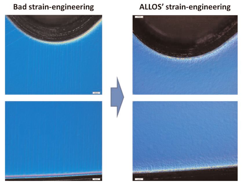
Technology focus: LEDs 49

light emission) are required. And of course, all these        traditionally a key driver for cost savings.
chips have to work after the display has been assembled,        Additionally, the cost per mask layer is actually higher
as consumers would not tolerate any pixels that are           in the LED industry compared with, for example,
dead or light up in the wrong color.                          200mm silicon foundries. This means that silicon
                                                              foundries not only produce many more chips per wafer
The problem with conventional                                 (due to the increased wafer size) but total cost per chip
LED technology                                                is significantly lower compared with in-house chip
Conventional blue and green LEDs are manufactured             making at LED companies. To make matters worse,
by specialized LED vendors using gallium nitride              LED companies would need to invest heavily to
(GaN)-on-sapphire epiwafers while red LEDs are                upgrade their fabs to larger diameters and to meet the
mostly based on aluminium gallium indium phosphide            precision and particle requirements which are not
(AlGaInP)-on-GaAs material. These technologies are            needed for conventional LEDs but are unavoidable for
mature for conventional LEDs and widely available.            micro-LED production.
Additionally, several color conversion technologies             In parallel, micro-LED manufacturing needs to address
could turn inexpensive GaN-based LEDs into red LEDs.          another even more severe issue: Due to inhomogeneity
One could thus expect that conventional LEDs are pro-         in the emission wavelength of the typical GaN-on-sapphire
viding a solid foundation for micro-LED chip production       LED epiwafer, each LED chip needs to be tested and
as well.                                                      sorted into one of several bins to ensure that the
  But, despite large investments by leading LED suppliers,    respective sub-pixel will emit the desired light color.
sapphire-based micro-LED manufacturing remains far            Already for conventional LEDs this represents a huge
from being ready for mass production. To start with,          cost burden, but when facing the 25 million chips for a
sapphire substrates are limited to 100mm and 150mm            4K display, this so-called ‘binning’ approach becomes
diameters, as larger substrates remain very expensive         technically impractical and cost-wise a show-stopper
and result in too much GaN-on-sapphire wafer bow.             for volume production. What is needed instead is an
Such wafer bow causes yield losses that eat up all            epiwafer technology that allows for the production of
theoretical cost savings of moving to larger diameters.       larger epiwafers resulting in low-cost micro-LED chips
This is in contrast to processes in the silicon semicon-      with better wavelength uniformity to avoid binning and
ductor industry, where going to larger substrates is          increase yield.

Figure 1: Cost & yield effects of ALLOS’ 1 bin® large-diameter GaN-on-Si LED epiwafers on entire production chain.

www.semiconductor-today.com                    semiconductor TODAY Compounds&AdvancedSilicon • Vol. 15 • Issue 3 • April/May 2020
50 Technology focus: LEDs
   High yield and low cost with
   GaN-on-Si based micro-LEDs
   To answer these demands for better
   emission wavelength uniformity and
   larger epiwafers, ALLOS Semiconductors
   of Dresden, Germany has developed its
   1 bin® LED epiwafer technology. Instead
   of sapphire, it uses a proprietary and
   patented hetero-epitaxial process to
   grow GaN on silicon (GaN-on-Si)
   substrates in a standard metal-organic
   chemical vapor deposition (MOCVD)
   reactor. When comparing ALLOS’
   GaN-on-Si with market-leading
   GaN-on-sapphire, both materials have
   the same crystal quality with threading
   dislocation density of 2x108cm–2 and
   thus allow the manufacturing of micro-
   LED chips with high emission efficiency.
   Also, the cost per mm2 epiwafer area
   before chip processing is similar.
   The key advantage of ALLOS’ 1 bin®
   GaN-on-Si technology is that it provides
   larger diameters and much better             Figure 2: Typical curvature profile during GaN-on-Si LED epi growth.
   uniformity. This allows the realization
   of huge cost and yield advantages along the entire            so-called transfer stamps, large wafers enable further
   production chain, as shown in Figure 1.                       cost-savings as the area utilization improves signifi-
     Driven by customer demand, ALLOS has worked                 cantly with larger wafer diameters. Comparing for
   mainly on 200mm but recently has also successfully            example 200mm with conventional 100mm wafers
   demonstrated its technology on 300mm wafers. Both             and assuming a transfer stamp size of 20mm x 20mm,
   wafer sizes enable the use of low-cost, high-yield silicon the total wafer area increases by a factor of four while
   processing lines for micro-LED chip manufacturing.            better area utilization allows for five times more usable
   This can be realized either by acquiring depreciated          chips. This better area utilization alone enables a
   200mm hardware or by sub-contracting chip process-            reduction of LED chip cost per display of 25%, which
   ing to foundries. This might also lead to new forms of        increases to a staggering 40% when migrating further
   cross-industry cooperation: While LED companies               to 300mm.
   could use their technological expertise and IP to design        Finally, using a silicon foundry and matching LED
   and deliver good micro-LEDs, the manufacturing                wafer sizes also offers the opportunity for integration
   excellence of silicon semiconductor companies in              with silicon technology processes, e.g. for the so-called
   delivering unmet yield levels at low cost plus their          monolithically integrated micro-LED displays, where
   available manufacturing capacity qualifies them as            CMOS driver wafers are bonded to LED wafers.
   perfect contributors to overcome the yield and cost
   challenges for micro-LED chip production.                     Precise strain engineering enabling
     To benefit from the advantages of standard silicon          large epiwafers
   processing lines the 1 bin® epiwafer technology is —          In light of these huge advantages of GaN-on-Si for
   unlike sapphire — fulfilling all incoming wafer quality       micro-LED production, the question arises how to
   criteria of CMOS lines. For example, the epiwafers are        achieve the necessary and decisive epiwafer properties.
   crack-free, thin (725µm at 200mm and 775µm at                 For ALLOS the technological answer lies in the strain
   300mm) and have only minimal bow (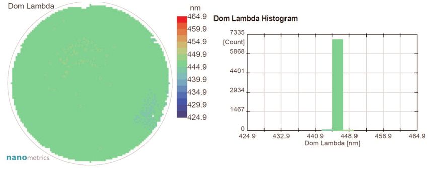
Technology focus: LEDs 51
Excellent and stable
wavelength uniformity
is essential for high yield
Achieving superior wavelength
uniformity is the key to address
the need for high yield, as
inhomogeneities on the
epiwafer level multiply
yield-losses throughout
the manufacturing chain.
There are two critical parame-
ters for achieving excellent
wavelength uniformity:
(1) temperature uniformity
across the epiwafer during
the multiple-quantum-well
(MQW) growth and
(2) gas flow uniformity inside
the MOCVD reactor.
The latter can be achieved
through gas flow simulation
and the use of latest-genera-
tion reactor types, like the
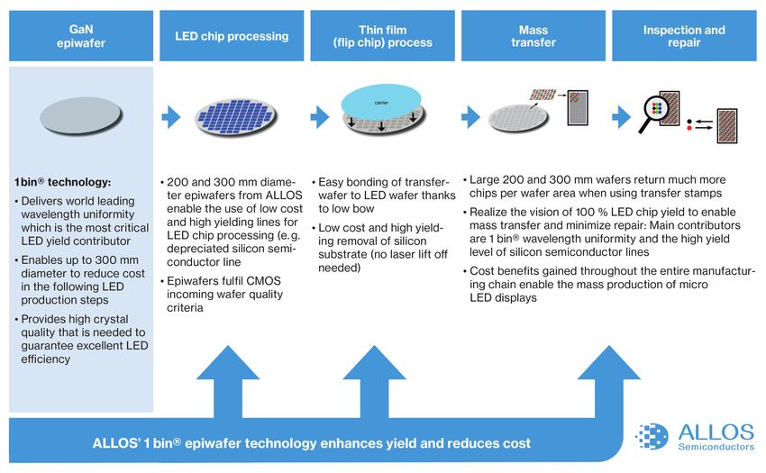
Figure 3: Nomarski images of notch and opposite round edge of 200mm Veeco Propel in the case of the
GaN-on-Si epiwafers. With ALLOS’ strain engineering cracks can be reliably data presented here. Achieving
prevented even at the very edge of the wafer which is otherwise often seen in good epiwafer temperature
GaN-on-Si growth (left image). uniformity is much more
difficult, as during MQW
there are several trade-offs between these attributes growth the epiwafer is convex (see Figure 2), resulting
and other LED properties, like wavelength uniformity in different distances between the heat source
— the crucial contributor to high yield. This means that underneath and the epiwafer above (large distance at
producing ‘hero results’ for individual parameters center and zero distance at the edge of the epiwafer).
might be possible even with immature technologies, This problem increases with epiwafer size, which
but the real challenge lies in achieving good values for makes it challenging to obtain good wavelength
all crucial properties at the same time. uniformity on 200mm and 300mm GaN-on-Si LED
Figure 2 shows the typical curvature profile of epiwafers.
GaN-on-Si during growth. When cooling down from In combination with a specially designed domed
growth temperature (~1000ºC) to room temperature, wafer carrier, which is dissipating heat uniformly,
huge tensile strain is induced into the structure. ALLOS is utilizing the power of its strain engineering to
With ALLOS’ strain engineering this is compensated control the shape of the epiwafer during MQW growth.
by purposely inducing a precisely defined amount of This ensures that the distance between the domed
compressive strain during growth. This results in flat wafer carrier and the epiwafer is equal across the
epiwafers after cooling down. Additionally, the epiwafer entire epiwafer diameter. The resulting temperature
bow during growth can be controlled with a high accu- uniformity leads to ALLOS’ industry-leading wave-
racy of ±5µm and can be adjusted to accommodate length uniformity values.
external factors too. If needed, this in-line process Figure 4 shows the photoluminescence (PL) map of
control capability can, for example, be used to adjust a 200mm GaN-on-Si LED epiwafer. The optimized
to unexpected shifts in the bow of the incoming growth conditions result in a standard deviation
substrate, as detected by an in-situ monitor at the (STDEV) of only 0.566nm at an average wavelength
beginning of the growth. The same strain engineering of 446.4nm. The wavelength histogram shows that
enables the growth on large diameters and is used 97.6% of the coverage area is within the 2.5nm target
to reliably prevent cracks (see Figure 3). It enables bin. The min-max value of wavelength for the entire
growing much thicker GaN layers (7µm and more) epiwafer is as low as 3.3nm. Even in the case that a
than competing technologies and delivers epiwafers further tightened ±1nm wavelength uniformity bin
that have the standard substrate thickness used in were applied, 92.1% of the epiwafer area is within
silicon lines (e.g. 725µm for 200mm). that target already today.
www.semiconductor-today.com semiconductor TODAY Compounds&AdvancedSilicon • Vol. 15 • Issue 3 • April/May 202052 Technology focus: LEDs
Dom Lambda nm
464.9 Dom Lambda Histogram
459.9
7335
454.9 [Count]
449.9 5868
444.9
4401
439.9
434.9 2934
429.9
1467
424.9
0
424.9 432.9 440.9 448.9 456.9 464.9
Dom Lambda [nm]
Figure 4: PL map of a 200mm GaN-on-Si LED epiwafer. Average wavelength of 446.4nm with STDEV of 0.566nm
is achieved. The histogram with 2.5nm bin size shows 97.6% coverage area and min-max value is 3.3nm.
Summary and outlook
2.4 While the industry’s prototypes are
impressively demonstrating that the
Emission wavelength STDEV (nm)
2.2
product features enabled by micro-LEDs
2.0 provide real customer benefits, the ques-
tion how high-yield and cost-competitive
1.8 mass production can actually be achieved
remains to be answered by the industry.
1.6
For this, a breakthrough in wavelength
1.4 uniformity is crucial, as otherwise low
yield levels will block the path forward.
1.2 However, even if that were achieved on
small wafer diameters, the cost would
1.0
remain prohibitive. Thus, the industry
0.8 needs to move to 200mm and 300mm
wafer diameters. Also, with large GaN-on-Si
0.6 epiwafers the micro-LED industry can
utilize the high-yield and low-cost
0.4
manufacturing excellence of silicon lines.
0 1 2 3 4 5 6 7 8 9 10 11 12 13 14 15 ALLOS’ 1 bin® LED epiwafer technology
LED epiwafer fulfills these essential requirements.
Based on the underlying proprietary and
Figure 5: Wavelength STDEV for 13 consecutive production runs of patented strain-engineering technology, it
200mm GaN-on-Si LED epiwafers. can provide 200mm and 300mm GaN-on-Si
LED epiwafers with best-in-industry
This uniformity figure is not only the best published wavelength uniformity values while simultaneously
worldwide – more importantly, this performance is meeting the performance requirements — and all other
reproducible, as shown by Figure 5 with data from 13 manufacturing requirements.
consecutive production runs of 200mm GaN-on-Si epi- Together with other breakthroughs — in mass transfer,
wafers. Thanks to ALLOS’ strain engineering, the epi- for example — we see that the foundations for micro-LED
wafer shape during MQW growth can be kept constant mass production are becoming a reality and will deliver
so that the wavelength uniformity becomes very stable exciting new consumer and business applications. ■
wafer-to-wafer. The average STDEV is 0.79nm and all
epiwafers have values below 1nm. At the same time, Authors: CEO Burkhard Slischka (bs@allos-semiconductors.com)
all other production requirements, such as for example CTO Dr. Atsushi Nishikawa (an@allos-semiconductors.com)
bow ofYou can also read