Establishing Traceability for On-Wafer S-Parameter Measurements of Membrane Technology Devices up to 110 GHz - PTB-OAR
←
→
Page content transcription
If your browser does not render page correctly, please read the page content below
© 2017 IEEE. Personal use of this material is permitted. Permission from IEEE must be obtained for all other uses, in any current or future media, including
reprinting/republishing this material for advertising or promotional purposes, creating new collective works, for resale or redistribution to servers or lists, or reuse of any
copyrighted component of this work in other works. The original publisher-authenticated version of this paper can be found at: https://doi.org/10.1109/ARFTG.2017.8255874 .
The following article is the final version submitted to IEEE after peer review; hosted by PTB; DOI: 10.7795/EMPIR.14IND02.CA.20190403 .

    Establishing Traceability for On-Wafer S-Parameter Measurements of
               Membrane Technology Devices up to 110 GHz

Uwe Arz1 , Sherko Zinal1 , Thorsten Probst1 , Gerd Hechtfischer2 , Franz-Josef Schmückle3 , and Wolfgang Heinrich3
                          1
                          Physikalisch-Technische Bundesanstalt (PTB), 38116 Braunschweig, Germany
                                   2
                                     Rohde & Schwarz GmbH & Co. KG, München, Germany
                    3
                      Ferdinand-Braun-Institut, Leibniz-Institut für Höchstfrequenztechnik, Berlin, Germany

   Abstract—In this paper we report on progress towards estab-
lishing traceability for fully calibrated on-wafer measurements of
planar devices built in membrane technology. For the first time,
we present a comprehensive uncertainty budget for on-wafer
S-parameter measurements, including instrumentation errors,
connector repeatability and calibration standard uncertainties.
Preliminary results are shown for three typical devices.
   Index Terms—on-wafer, calibration, S-parameters, traceability,
uncertainty budget.

                              I. I NTRODUCTION
   In contrast to coaxial and rectangular waveguide S-
parameter measurements, traceability for on-wafer S-
parameters has not been fully established yet. This is because                           Fig. 1. Thru calibration standard fabricated in membrane technology.
planar devices and calibration standards are fabricated on                                                         II. T ECHNOLOGY
different substrate materials in a great variety of technologies,
and instead of standardized connectors nowadays a number                                 The membrane technology CPWs were fabricated on
of microwave probes from several vendors can be used.                                 double-side-polished high-resistivity  silicon wafers. In
Therefore, reliable uncertainties for on-wafer S-parameters                           the first step, a thin film of silicon dioxide (SiO2 ) is deposited
can only be specified in a given enviroment for selected                              on both sides of the high-resistivity silicon (HRSi) wafer
combinations of substrate materials, planar waveguides, and                           by plasma-enhanced chemical vapor deposition (PECVD) to
probes.                                                                               form an etching barrier. This is followed by the deposition of
   The evaluation of S-parameter uncertainty depends on a                             a thin layer of PECVD silicon nitride (Si3 N4 ) as dielectric
number of factors such as instrumentation errors, cable and                           membrane. Multi-frequency plasma-enhanced chemical vapor
connector repeatability, standard uncertainties, the calibration                      deposition is used to minimize the mechanical stress within
algorithm chosen, and the DUT itself. This complicated task                           the membrane layer. After the deposition of the dielectric
is greatly simplified with modern software tools such as [1] or                       material, a thin adhesive layer of titanium-tungsten (TiW) and
[2], which have been recently compared in [3] and [4]. In our                         a gold (Au) layer is sputtered on the top side of the wafer.
approach, we established a comprehensive uncertainty budget                           The conductor geometry is then formed by optical lithography
for the entire measurement process using the linear uncertainty                       and wet chemical etching processes. Subsequently, using an
propagation library Metas.UncLib [5], which is based on the                           appropriate photoresist mask, openings in top side silicon
automatic differentiation techniques of [6].                                          dioxide and silicon nitride layers are patterned by dry and
   In this paper we focus on planar devices built in membrane                         wet chemical etching processes.
technology, as the influence of the thin supporting dielec-                              The final step is the partial removing of the silicon wafer
tric material is significantly reduced in comparison to the                           itself to create silicon nitride membranes under the conductor
influence of several-hundred-µm thick substrates which are                            geometry. Openings are structured on the back side silicon
conventionally used. In essence, membrane technology enables                          dioxide and silicon nitride. Anisotropic etching of the silicon
us to employ air-line-like coplanar waveguides (CPWs) as                              wafer from the back side is done with a potassium hydroxide
calculable calibration standards [7].                                                 solution, leaving the dielectric membrane carrying the CPW
   In the following sections, we outline the technology steps                         line structure.
required, describe modeling and characterization of the airline-                         Figure 1 shows an interconnect structure serving as Thru
like CPW standards and the measurement setup, give an                                 calibration standard consisting of silicon-to-membrane tran-
overview of the input quantities considered in the uncertainty                        sitions at both sides of a CPW section supported by a thin
budget, and show some preliminary results.                                            membrane. The silicon-to-membrane transitions contain con-
tact pads, which allow for ground-signal-ground microwave
probing, and a short interconnect segment on silicon.
III. CPW M ODELING AND C HARACTERIZATION
Figure 2 shows the cross section of a coplanar airline
resulting from the technology described in the previous section
together with its geometrical and material parameters.
wg s w s wg
εr,mem Si3N4 tmem
t κ membrane
tanδ Fig. 3. VNA measurement model (from [2]).
Si
VNA, the noise/linearity influences, the switch terms, the drift
h of the switch terms, the calibration error terms, the drift of the
calibration error terms, the cable stability/connector repeata-
bility and DUT uncertainty influences, and the error corrected
Fig. 2. Cross section of CPW built in membrane technology.
data (or calibration kit standard definitions), respectively.
To calculate the wideband electromagnetic properties of the The error terms of the underlying 7-term error model
CPW, we used the extension of the model of [8] introduced were calculated with the multiline TRL calibration algorithm
in [9]. In [9] the effect of the membrane is taken into account described in [13] and [14]. Seven lines with membrane CPW
by using equivalent dielectric material values εr, LHP and lengths between 500 and 20190 µm were used, assuming a
tan δLHP of a fictitious infinitely-expanded lower half-plane length uncertainty of 10 µm.
(LHP). The value of the dielectric constant εr, mem of the Since the multiline TRL method, as a self-calibration
membrane material was estimated in previous studies [10]. technique, does not allow for a straightforward propagation
Propagation constant and characteristic impedance of the of calibration standard uncertainties, the influence of these
fabricated CPW lines were calculated with both the model uncertainties was calculated using the Microwave Uncertainty
of [8] and the extended model of [11], which considers Framework developed at NIST [1]. In future studies we will
modal dispersion and radiation losses. However, no indications compare these calculations to the results of the recursive
of modal dispersion or radiation losses were found in the approaches described in [15] and [16].
frequency range under investigation.
V. I NPUT Q UANTITIES
Table I shows the cross-section parameters obtained for
the membrane CPW part according to Fig. 1 after performing In the following, most input quantities relevant for the
the dimensional and material characterization at PTB. Dimen- measurement process are listed with their respective values
sional characterization was carried out with a high-precision and/or uncertainties (coverage factor is k=2 unless indicated
optical coordinate measuring machine and an atomic-force otherwise). They are typical for the on-wafer measurement
microscope. setup used at PTB for frequencies up to 120 GHz. Mea-
surements were performed on a ceramic chuck utilizing an
TABLE I Anritsu VectorStar VNA with mm-wave extension modules
Parameters of membrane CPW on HRSi.
for frequencies up to 125 GHz, connected to GGB ground-
Parameter value signal-ground microwave probes with 100 µm pitch.
wg (408.6 ± 0.5) µm Cable movement was not considered, as the 1-mm cables
w (168.7 ± 0.5) µm connecting to the GSG probes were fixed during the measure-
s (6.3 ± 0.5) µm
t (0.550 ± 0.05) µm
ments. The movement of the cables leading to the mm-wave
k (16.5 ± 1) MS/m extensions essentially affects only measurements up to 30 GHz
εr, LHP (1.706 ± 0.1) and is currently neglected.
tmem 1.2 µm
tan δLHP (1 ± 0.5) · 10−4 A. VNA Characterization
h 295 µm
1) Noise and Error Term Drift: VNA characterization was
performed following the procedures outlined in [12]. Due to
IV. VNA M EASUREMENT M ODEL AND C ALIBRATION
space limitations, the values used have been omitted.
For the calculation of corrected S-parameters from the 2) Linearity: The uncertainty in linearity was estimated to
measured raw data and the propagation of measurement as the values of 0.01 dB for the magnitude and 0.066◦ for the
well as calibration standard uncertainties to the final results, phase over the used magnitude and frequency range.
the VNA measurement model described in [12] and [2] has
been applied. B. Connector Repeatability
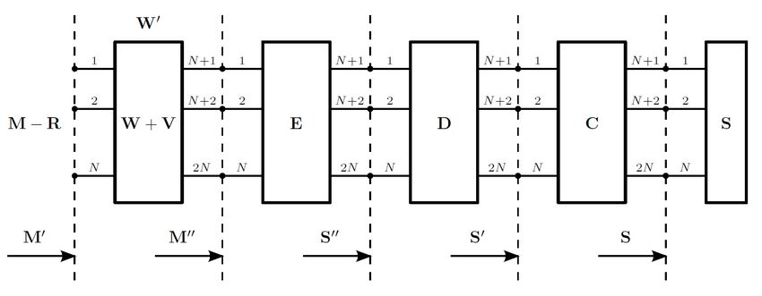
Figure 3 shows a block diagram of the general N-port Connector repeatability has been considered with an uncer-
measurement model (in our case N=2). The symbols M, R, tainty of -60 dB. This value was determined from a series of
W, V, E, D, C and S denote the the raw data measured by the repeat measurements.C. DUT Uncertainty/Crosstalk VII. DUT U NCERTAINTY R ESULTS
Due to the lack of resistive elements in the current mem- In the following results for three typical devices are shown,
brane wafer, the crosstalk correction of [17] could not be covering a large portion of the impedance range measurable
applied. Instead, the DUT uncertainty approximation as de- by a VNA: a 20190 µm-long matched line (termed ‘match’) ,
scribed in [2] has been employed. For the sake of brevity, the a 7065 µm-long mismatched line (termed ‘mismatch’), and a
values used in the approximation are not shown here. 2-port open (high-reflect device, termed ‘open’)).
D. Calibration Standards TABLE II
Preliminary uncertainty budget for magnitude of S11 (linear) at 55 GHz.
The influence of the uncertainties in the calibration standard
uncertainties was calculated using the Microwave Uncertainty Device match mismatch open
Framework [1] and the values indicated in Table I. Value 0.03663 0.47942 0.99603
Standard Uncertainty 0.01216 0.00559 0.00346
VI. M EASUREMENT-M ODEL C OMPARISON Description Unc. comp. Unc. comp. Unc. comp.
Calibration Standards 0.01214 0.00555 0.00320
Figure 4 compares measured and model-based values of Connector Repeatability 0.00051 0.00060 0.00066
reflection and transmission S-parameters of a 500 µm-long DUT Uncertainty 0.00007 0.00023 < 10−5
matched line. Solid lines indicate nominal values, shaded VNA Drift 0.00047 0.00037 0.00112
VNA Linearity < 10−5 0.00001 0.00004
areas indicate the expanded uncertainty intervals at a coverage VNA Noise 0.00002 0.00003 0.00005
probability of 95% (k=2). The S-parameters are normalized to
50 Ω. The expanded uncertainty intervals fully comprise the TABLE III
model values in the frequency range from 1 to 110 GHz. Preliminary uncertainty budget for phase of S11 (degrees) at 55 GHz.
Device match mismatch open
Value -32.91004 -72.35470 -40.48126
Standard Uncertainty 7.19505 1.22936 1.29353
Description Unc. comp. Unc. comp. Unc. comp.
Calibration Standards 7.11245 1.22219 1.27407
Connector Repeatability 0.79520 0.07083 0.03819
DUT Uncertainty 0.11457 0.02784 < 10−5
VNA Drift 0.73194 0.10839 0.22017
VNA Linearity < 10−5 0.00139 0.00238
VNA Noise 0.02499 0.00520 0.00514
TABLE IV
Preliminary uncertainty budget for magnitude of S21 (linear) at 55 GHz.
Device match mismatch open
Value 0.43230 0.77150 0.00732
Standard Uncertainty 0.00288 0.00749 0.00838
Description Unc. comp. Unc. comp. Unc. comp.
Calibration Standards 0.00056 0.00555 0.00020
Connector Repeatability 0.00001 0.00025 < 10−5
DUT Uncertainty 0.00281 0.00501 0.00838
VNA Drift 0.00032 0.00030 < 10−5
VNA Linearity < 10−5 0.00003 < 10−5
VNA Noise 0.00002 0.00004 < 10−5
TABLE V
Preliminary uncertainty budget for phase of S21 (degrees) at 55 GHz.
Device match mismatch open
Value -149.72412 -168.66761 -49.69122
Standard Uncertainty 1.00119 1.21283 32.44710
Description Unc. comp. Unc. comp. Unc. comp.
Calibration Standards 0.91378 1.15114 2.14989
Connector Repeatability 0.00184 0.01853 0.03814
DUT Uncertainty 0.37232 0.37235 32.37532
VNA Drift 0.16952 0.08251 0.16988
VNA Linearity 0.00060 0.00197 < 10−5
VNA Noise 0.00577 0.00609 0.01985
A. Uncertainty budgets
For the three selected devices, the preliminary uncertainty
budgets for magnitude and phase of S11 and S21 are listed in
Fig. 4. Comparison between measured (black) and modeled (blue) reflection
and transmission S-parameters of a 500 µm-long matched line. Tables II – V for the intermediate frequency of 55 GHz. Inmost cases the budget is dominated by the calibration standard ACKNOWLEDGMENT
uncertainties. In the magnitude and phase of S21 , the influence The authors thank K. Kuhlmann, D. Schubert, T. Dziomba
of the DUT uncertainty approximation becomes dominant at and D. Schulz from PTB for their expert technical assistance.
increasing frequencies for medium- to high-reflect devices. The authors acknowledge support by the European Metrol-
At low frequencies (not shown here), VNA drift can become ogy Programme for Innovation and Research (EMPIR) Project
significant for matched devices. 14IND02 “Microwave measurements for planar circuits and
B. Expanded uncertainties components”. The EMPIR program is co-financed by the par-
Figure 5 shows expanded uncertainty intervals at a coverage ticipating countries and from the European Union’s Horizon
probability of 95% (k=2) of reflection and transmission S- 2020 research and innovation program.
parameters for all three devices considered.
R EFERENCES
[1] D. F. Williams, “NIST Microwave Uncertainty Framework,
Beta Version,” www.nist.gov/services-resources/software/
wafer-calibration-software, 2012.
[2] M. Wollensack and J. Hoffmann, “METAS VNA Tools II - Math
Reference V1.8,” www.metas.ch, 2017.
[3] V. Teppati and A. Ferrero, “A Comparison of Uncertainty Evaluation
Methods for On-Wafer S-Parameter Measurements,” IEEE Trans. In-
strum. Meas., vol. 63, no. 4, pp. 935–942, April 2014.
[4] G. Avolio, D. F. Williams, S. Streett, M. Frey, D. Schreurs, A. Ferrero,
and M. Dieudonné, “Software tools for uncertainty evaluation in VNA
measurements: A comparative study,” in 2017 89th ARFTG Microwave
Measurement Conference (ARFTG), June 2017, pp. 1–7.
[5] M. Zeier, J. Hoffmann, and M. Wollensack, “Metas.UncLib—A mea-
surement uncertainty calculator for advanced problems,” Metrologia,
vol. 49, no. 6, p. 809, 2012.
[6] B. D. Hall, “Calculating measurement uncertainty using automatic
differentiation,” Measurement Science and Technology, vol. 13, no. 4,
p. 421, 2002.
[7] U. Arz, M. Rohland, and S. Büttgenbach, “Improving the Performance of
110 GHz Membrane-Based Interconnects on Silicon: Modeling, Mea-
surements, and Uncertainty Analysis,” IEEE Trans. Compon. Packag.
Manuf. Technol., vol. 3, no. 11, pp. 1938–1945, Nov 2013.
[8] W. Heinrich, “Quasi-TEM description of MMIC coplanar lines including
conductor-loss effects,” IEEE Trans. Microwave Theory Tech., vol. 41,
no. 1, pp. 45–52, Jan. 1993.
[9] U. Arz, M. Rohland, K. Kuhlmann, and S. Büttgenbach, “Wideband
Electromagnetic Modeling of Coplanar Waveguides Fabricated in Mem-
brane Technology,” in 15th IEEE Workshop on Signal Propagation on
Interconnects, May 2011, pp. 129–130.
[10] U. Arz, M. Rohland, K. Kuhlmann, and S. Büttgenbach, “Optimized
Coplanar Waveguides in Membrane Technology for Wideband On-Wafer
Calibrations,” in 20th IEEE Conference on Electrical Performance of
Electronic Packaging & Systems, Oct. 2011, pp. 77–80.
[11] F. Schnieder, T. Tischler, and W. Heinrich, “Modeling Dispersion
and Radiation Characteristics of Conductor-Backed CPW With Finite
Ground Width,” IEEE Trans. Microwave Theory Tech., vol. 51, no. 1,
pp. 137–143, Jan. 2003.
[12] EURAMET CG-12, “Guidelines on the Evaluation of Vector Net-
work Analysers (Draft Version 3.1),” www.metas.ch/metas/en/home/
fabe/hochfrequenz/Documents.html, 2017.
[13] R. B. Marks, “A Multiline Method of Network Analyzer Calibration,”
IEEE Trans. on Microwave Theory and Techniques, vol. 39, no. 7, pp.
1205–1215, 1991.
[14] D. C. DeGroot, J. A. Jargon, and R. B. Marks, “Multiline TRL
Revealed,” in 60th ARFTG Conference Digest, Fall, Washington, DC,
USA, 2002, pp. 131–155.
Fig. 5. Expanded uncertainty intervals at a coverage probability of 95% (k=2). [15] U. Stumper, “Uncertainty of VNA S-Parameter Measurement Due to
Nonideal TRL Calibration Items,” IEEE Trans. on Instrumentation and
Measurement, vol. 54, no. 2, pp. 676–679, 2005.
VIII. C ONCLUSIONS [16] B. Hall, “On evaluating the uncertainty of VNA self-calibration pro-
For the special case of membrane technology devices, cedures,” in First workshop on “Electronic Calibration Units” and
European ANAMET meeting, Dec. 2013.
we presented a comprehensive uncertainty budget for on- [17] D. F. Williams, F. J. Schmückle, R. Doerner, G. N. Phung, U. Arz, and
wafer S-parameter measurements. Traceability to dimensional W. Heinrich, “Crosstalk Corrections for Coplanar-Waveguide Scattering-
measurements was demonstrated for selected devices in the Parameter Calibrations,” IEEE Trans. Microw. Theory Techn., vol. 62,
no. 8, pp. 1748–1761, Aug 2014.
frequency range from 1 to 110 GHz. Current and future [18] European Metrology Programme for Innovation and Research JRP
research [18] will extend the methodology presented in this Number 14IND02, “Microwave measurements for planar circuits and
paper to other substrate materials and probe configurations. components.” https://planarcal.ptb.de.You can also read