GREEDY SNAKE VIDEO GAME BASED ON NIOS II SYSTEM - Jinpeng Li - Technology and Communication 2014
←
→
Page content transcription
If your browser does not render page correctly, please read the page content below
Jinpeng Li

GREEDY SNAKE VIDEO GAME
 BASED ON NIOS II SYSTEM

    Technology and Communication

               2014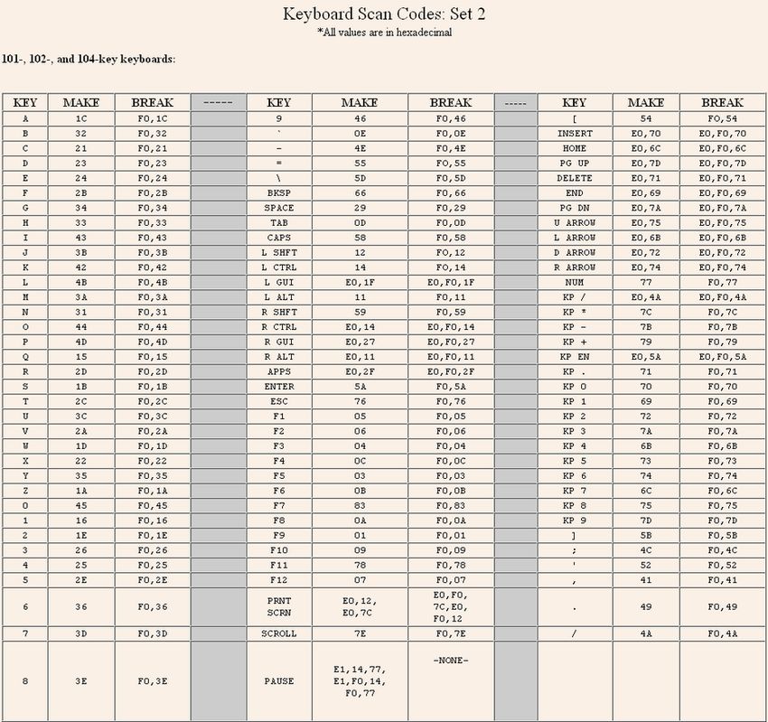
1

FOREWORD

I would like to give my greatest gratitude to the people who helped me during
working on this thesis topic. First, I would like to thank for the guide and courage
given by my supervisor Santiago Chávez Vega, Senior Lecturer of VAMK. And I
would like to thank for the advice from my friends. Finally, I would to give my thanks
to my family in China and my girlfriend who keeps company with me all the time.

Li Jinpeng

Vaasa, Finland
24, March, 2014
2

VAASAN AMMATTIKORKEAKOULU
UNIVERSITY OF APPLIED SCIENCES
Degree Program in Information Technology

ABSTRACT

Author         Jinpeng Li
Title          Greedy Snake Video Game Based on Nios II System
Year           2014
Language       English
Pages          57+6 Appendices
Name of Supervisor Santiago Chávez Vega

With the development of large scale integrated circuit, traditional embedded system
design method cannot meet the requirements for building complex systems. Therefore,
SOC and SOPC technology are widely used nowadays. This thesis aims to
development a game platform based on Nios II system using Altera DE2 development
and education board and SOPC technology. In this thesis, first a custom Nios II
system was built according to the requirements of the game application. The system
contains hardware interfaces for VGA and PS/2 device. Second, the Greedy Snake
game was developed using the C programming language. The game is shown on a
LCD monitor and controlled by a PS/2 keyboard. At last, the designed Nios II system
and the game application were downloaded into the DE2 board. Through the test by
different players, the system and the game perform well.

Keywords                 Nios II, VGA, PS/2, DE2, Greedy Snake
3

TABLE OF CONTENTS

FOREWORD................................................................................................................ 1
ABSTRACT .................................................................................................................. 2
LIST OF FIGURES ..................................................................................................... 5
LIST OF TABLES ....................................................................................................... 7
LIST OF ABBREVIATIONS ..................................................................................... 8
1 INTRODUCTION..................................................................................................... 9
      1.1 Research Content of the Thesis ......................................................................... 9
      1.2 Background ..................................................................................................... 10
            1.2.1 SOC and SOPC Technology ................................................................. 10
            1.2.2 Nios II Processor ................................................................................... 10
            1.2.3 Avalon Switch Fabric ............................................................................ 11
      1.3 Thesis Outline ................................................................................................. 11
2 THEORETICAL STUDY ...................................................................................... 12
      2.1 VGA ................................................................................................................ 12
            2.1.1 VGA Introduction ................................................................................. 12
            2.1.2 VGA Principle ....................................................................................... 12
            2.1.3 VGA Timing Analysis ........................................................................... 14
            2.1.4 VGA Interface ....................................................................................... 16
            2.1.5 RGB Color Model ................................................................................. 17
      2.2 PS/2 ................................................................................................................. 18
            2.2.1 PS/2 Interface ........................................................................................ 18
            2.2.2 PS/2 Protocol and Data Format............................................................. 20
            2.2.3 PS/2 Keyboard ...................................................................................... 23
            2.2.4 Scan Code Set ....................................................................................... 23
      2.3 Data and Memory Layout in Qsys .................................................................. 25
3 SYSTEM DESIGN AND BUILDING ................................................................... 28
      3.1 Tools ................................................................................................................ 28
            3.1.1 Altera DE2 Development and Education Board ................................... 28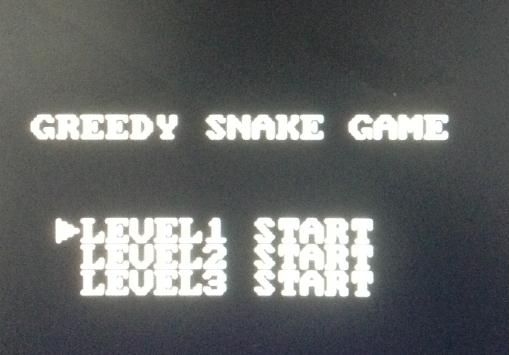
4

            3.1.2 Quartus II Design Software .................................................................. 28
            3.1.3 Qsys System Integration Tool ............................................................... 29
      3.2 System Hardware Design ................................................................................ 30
            3.2.1 System Requirements Analysis ............................................................. 31
            3.2.2 Defining and Generating the System in Qsys ....................................... 32
            3.2.3 Integrate Qsys System into Quartus II Project ...................................... 49
            3.2.4 Pin Assignment and Hardware Design Compiling ............................... 49
4 GAME DEVELOPMENT ...................................................................................... 50
      4.1 Game Introduction .......................................................................................... 50
      4.2 Game Design ................................................................................................... 50
            4.2.1 Game Menu ........................................................................................... 50
            4.2.2 Game Logic ........................................................................................... 52
5 CONCLUSION ....................................................................................................... 55
REFERENCES ........................................................................................................... 56
APPEARANCE. VHDL SAMPLE CODE .............................................................. 58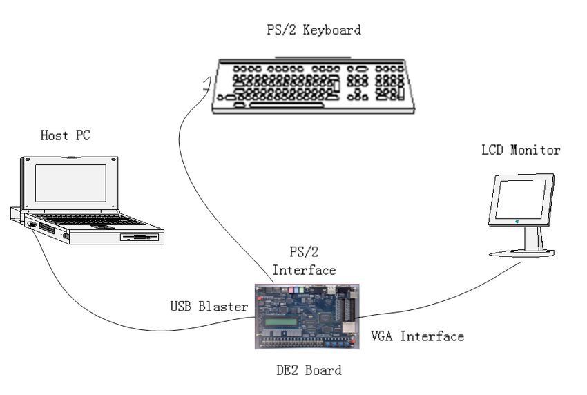
5

LIST OF FIGURES

   Figure 1.Required Devices and Collections ........................................................... 9
   Figure 2. Progressive Scan ................................................................................... 13
   Figure 3. Interlaced Scan ..................................................................................... 13
   Figure 4. VGA Horizontal Timing ....................................................................... 14
   Figure 5. VGA Vertical Timing ........................................................................... 15
   Figure 6. VGA Interface Layout .......................................................................... 16
   Figure 7. RGB Color Representation ................................................................... 18
   Figure 8. Pin Layout for PS/2 Interface ............................................................... 19
   Figure 9. A General OC Circuit ........................................................................... 20
   Figure 10. Waveform of One Data Frame from PS/2 Device to Host ................. 22
   Figure 11. Waveform of One Data Frame from Host to PS/2 Device ................. 23
   Figure 12. Scan Code for an US English Layout Keyboard ................................ 24
   Figure 13. Screen Layout of Image Frame .......................................................... 25
   Figure 14. Image Frame with Resolution of 640 x 480 ....................................... 26
   Figure 15. Consecutive Mode Mapping ............................................................... 27
   Figure 16. Consecutive Mode Mapping for Resolution of 640 x 480 ................. 27
   Figure 17. X-Y Mode Mapping ........................................................................... 27
   Figure 18. 16-bit Wide Color Address Mapping ................................................. 27
   Figure 19. 32-bit Wide Color Address Mapping ................................................. 27
   Figure 20. Altera DE2 Development and Education Board................................. 28
   Figure 21. Quartus II Software Web Version 13.0 .............................................. 29
   Figure 22. Qsys System Integration Tool ............................................................ 30
   Figure 23. Typical Development Flow for Nios II System ................................. 31
   Figure 24. Required Devices and Collections ...................................................... 32
   Figure 25. Qsys IP Cores Libbrary ...................................................................... 33
   Figure 26. Configuration for Nios II Processor ................................................... 34
   Figure 27. SDRAM Signals ................................................................................. 34
   Figure 28. Configuration for SDRAM Memory Profile ...................................... 35
6

Figure 29. Configuration for SDRAM Timing .................................................... 35
Figure 30. Block Diagram of Clock Signal IP Core ............................................ 36
Figure 31. Configuration for Clock IP Core ........................................................ 37
Figure 32. Configuration for Single Clock Source .............................................. 37
Figure 33. Configuration for SRAM Controller .................................................. 39
Figure 34. Pixel Buffer DMA Controller Configuration ..................................... 40
Figure 35. Configuration for Scaler ..................................................................... 40
Figure 36. Configuration for RGB Resampler ..................................................... 41
Figure 37. Configuration for Character Buffer for VGA Display ....................... 42
Figure 38. Configuration for Alpha Blender ........................................................ 43
Figure 39. Configuration for Dual-Clock FIFO ................................................... 44
Figure 40. Block Diagram of VGA Controller .................................................... 44
Figure 41. VGA Controller Configuration ........................................................... 45
Figure 42. Configuration for PS/2 Controller ...................................................... 45
Figure 43. Configuration for Interval Timer ........................................................ 46
Figure 44. Base Address and Interrupt Number Assignment .............................. 47
Figure 45. System Collection ............................................................................... 48
Figure 46. Integrating Nios II System to Quartus II Project ................................ 49
Figure 47. Game Menu Display ........................................................................... 51
Figure 48. Game Menu Flow Diagram ................................................................ 51
Figure 49. Menu Key Controlling for Selecting the Level .................................. 52
Figure 50. Initial Image Frame ............................................................................ 53
Figure 51. Game Logic Flow Diagram ................................................................ 54
7

LIST OF TABLES

   Table 1.VGA Timing Parameters Table for Popular Resolution ......................... 16
   Table 2.VGA Interface Pin Table ........................................................................ 17
   Table 3.PS/2 Pin Table ......................................................................................... 19
   Table 4.State of PS/2 Data Transmisson .............................................................. 20
   Table 5.PS/2 Data Frame Format ......................................................................... 21
   Table 6.Set 2 Make Code and Break Code for Some Keys ................................. 24
   Table 7.Scan Code Set 2 ...................................................................................... 25
   Table 8.Clock Signals Description ....................................................................... 36
   Table 9.Base Address and Interrupt Number Table ............................................. 47
   Table 10.Key Function for Controlling Game Logic ........................................... 54
8

LIST OF ABBREVIATIONS

ADC           Analog to Digital Converter

CPU           Central Processing Unit

CRT           Cathode Ray Tube

DMA           Direct Memory Access

DAC           Digital to Analog Converter

FIFO          First Input First Output

FPGA          Field Programmable Gate Array

HEX           Hexadecimal

I/O           Input and Output

IP            Intellectual Property

LSI           Large Scale Integration

LCD           Liquid Crystal Display

OC            Open Collector

PC            Personal Computer

PS/2          Personal System 2

RGB           Red Green Blue

RISC          Reduced Instruction Set Computing

SOC           System on Chip

SOPC          System on Programmable Chip

SDRAM         Synchronous Dynamic Random-Access Memory

SRAM          Static Random-Access Memory

SYNC          Synchronization

VGA           Video Graphics Array
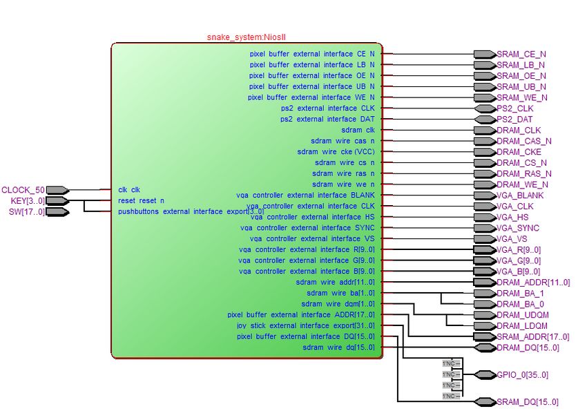
9 1 INTRODUCTION 1.1 Research Content of the Thesis This thesis project aims to build a game platform based on Nios II system and develop a video game application on the platform using Altera DE2 FPGA Educational Board. The project consists of two steps: Nios II System Architect Design and Building; Greedy Snake Game Development; During the first step, the Nios II system for the game platform was built using Quartus II and Qsys Tool. The system contains: One Nios II processor, Memory Unit, VGA control IP Core Unit, PS/2 controller IP Core and one Timer IP Core. Each component was configured according to the design requirements and collected to Nios II processor through Avalon switch fabric. During the second step, Greedy Snake Game was developed using C language. Figure 1 shows the required devices and collections of the system. Figure 1.Required Devices and Collections
10

1.2 Background

With the development of LSI and the increase of logical gates in one single chip,
embedded system design is becoming increasingly complex. Conventional design
methods cannot meet the requirements for today’s embedded systems. The
disadvantages of traditional developing method for embedded system are: difficult to
debug, relatively higher cost and long developing duration. A new developing method
called “Rapid Prototyping Technology” has gained great popularity in recent years. A
rapid prototyping design can be made easily using SOC technology. With this
technology, embedded system can be designed rapidly and modified easily. The cost
can be reduced and the developing circle can be shortened.

1.2.1 SOC and SOPC Technology

SOC is the technology to integrate a complete system into one single chip including
CPU, memory units, I/Os and peripheral units./1/ SOPC is a flexible and efficient
SOC design methodology, which integrates system into one chip using programmable
logic technology. The SOPC system is programmable and it can be designed with
great flexibility. The SOPC system contains at least one embedded processor core.
Functional blocks or IP Cores can be added to the system according to the
requirements of design, which makes it possible for designers to build a suitable
embedded system.

1.2.2 Nios II Processor

The Nios II Processor is the most widely used soft processor developed by Altera
Corporation. It is a 32-bit RISC soft core based on SOPC. It is implemented entirely
in the programmable logic and memory blocks of Altera FPGAs. The Avalon switch
fabrics are used as an interface between the soft core and its peripherals. System
designers can generate custom Nios II core through Quartus II platform with SOPC
Builder or Qsys Tool. These tools provide configurable IP Cores such as cache
module, RS232 communication port, SDRAM controller, standard Ethernet interface,
11 DMA and timers, which can extend the Nios II function./2/ The advantages of Nios II Processor are: More flexibility High performance Lower system cost High bandwidth bus structure Fast configurable IP Cores 1.2.3 Avalon Switch Fabric The Avalon switch fabric is a high-bandwidth interconnection structure developed by Altera Corporation. It is an on-chip bus technology collecting components in a system based on the Avalon interface using simple protocol. In the Nios II system, all peripheral units are collected to the Nios II processor through the Avalon switch fabric which is generated automatically by the SOPC Builder and Qsys tool. The main advantages of the Avalon switch fabric are: minimal logic resources consumption and greater flexibility./3/ 1.3 Thesis Outline This paper proceeds as follows: Chapter 1 introduces the background of this research topic. Chapter 2 gives description of theoretical study of the topic. Chapter 3 illustrates the Nios II system design. Chapter 4 explains the Greedy Snake Game development in detail. Chapter 5 draws conclusions and acknowledgement.
12

2 THEORETICAL STUDY

2.1 VGA

2.1.1 VGA Introduction

VGA is a computer display standard developed by IBM company in 1987. It is widely
used in color displays because it has high resolution, high refresh rate and color
diversity. VGA supports 16 colors or 256 gray scales at the resolution of 640x480 and
256 colors at the resolution of 320x240.

2.1.2 VGA Principle

A colorful image is generated when the electron beam from a cathode ray tube hits the
fluorescent screen. To generate an image, the screen will be scanned by the electron
beam. The scan mode can be divided into progressive scan and interlaced scan.

The progressive scan begins from the top left corner of the screen and it scans point
by point from left to the right of one line. After one line is scanned, the electron beam
moves back to the left start point of the next line and the beam is synchronized by
horizontal synchronization signal. During this movement, the cathode ray tube blanks
the electron beam. The beam scans the screen line by line until it reaches to the
bottom right corner of the screen. After all lines scanned, the beam moves back to the
top left corner of the screen and the beam is synchronized by horizontal
synchronization signal. During this movement also, the cathode ray tube blanks the
electron beam. At this point, an image frame is generated. Figure 2 shows the
progressive scan.

The interlaced scanning scans every other line of the screen. After the screen is
scanned once, the electron beam returns to scan the rest lines. Figure 3 shows the
interlaced scan.
13

Figure 2. Progressive Scan

Figure 3. Interlaced Scan
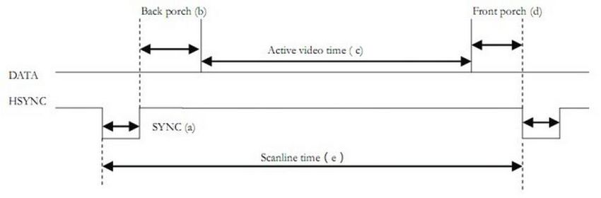
14

2.1.3 VGA Timing Analysis

VGA Timing includes horizontal timing and vertical timing. Both the horizontal
timing and vertical timing contain Synchronization Pulse, Back Porch, Display
Interval and Front porch./4/

At the beginning of the horizontal timing, a negative pulse is generated for horizontal
synchronization. It represents the end of one line and the start of the next line. After
the synchronization pulse is the back porch. During the display interval, RGB data
drives pixels of one line, generating one line of an image. At the end of a line there is
the front porch. The image is only displayed during the display interval. The
synchronization pulse, back porch, and front porch are in the Horizontal Blanking
Interval during which the RGB data is invalid and the image is not displayed on the
screen. Figure 4 illustrates the VGA horizontal timing.

a:   SYNC (Synchronization Pulse)

b:   Back Porch

c:   Active Video Time (Display Interval)

d:   Front Porch

e:   Scanline Timee = a+b+c+d

Figure 4. VGA Horizontal Timing
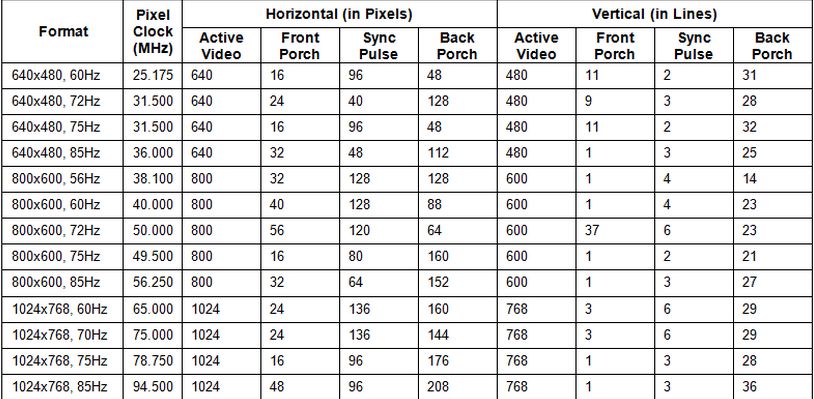
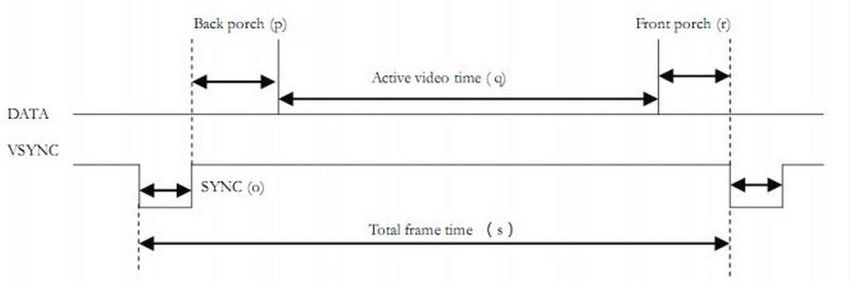
15

The VGA vertical timing is basically the same as the VGA Horizontal Timing. The
difference is that vertical synchronization pulse represents the end of one image frame
and the start of the next frame. The RGB data during display interval includes all lines
of the screen. Figure 5 demonstrates the VGA vertical timing.

o:   SYNC (Synchronization Pulse)

p:   Back Porch

q:   Active Video Time (Display Interval)

r: Front Porch

s:   Total Frame Time

s = o+p+q+r

Figure 5. VGA Vertical Timing

VGA timing parameters vary at different resolutions. Table 1 lists VGA timing
parameters for some popular resolutions.
16

Table 1.VGA Timing Parameters Table for Popular Resolution

2.1.4 VGA Interface

The VGA interface is a D-Type interface with fifteen pins. It has three lines and each
line has five pins as shown in Figure 6. Table 2 explains the definition and description
for each pin. The most important pins are:

Three video pins—Red, Green and Blue Video output pins;

Two synchronization output pins—Horizontal Sync and Vertical Sync pins/5/

Figure 6. VGA Interface Layout
17 Table 2.VGA Interface Pin Table Pin Number Name Direction Description 1 RED OUT Red Video 2 GREEN OUT Green Video 3 BLUE OUT Blue Video 4 ID2 IN Monitor ID Bit 2 5 GND — Ground 6 RGND — Red Ground 7 GGND — Green Ground 8 BGND — Blue Ground 9 KEY — KEY (No Pin) 10 SGND — Sync Ground 11 ID0 IN Monitor ID Bit 0 12 ID1 IN Monitor ID Bit 1 13 HSYNC or CSYNC OUT Horizontal Sync or Composite 14 VSYNC OUT Vertical Sync 15 ID3 IN Monitor ID Bit 3 2.1.5 RGB Color Model RGB Color Model is an additive color model. It generates various colors by adding three basic colors—red, green and blue, as shown in Figure 7. A color can be represented by how much each of the three basic colors is included./6/ Each of the three basic colors is one color component of the represented color. It can be concluded by the following expression: color f (r , g , b) The color is one particular color to be represented, and r, g, b are the three basic color components for red, green and blue respectively. The value of a color component can be defined in a predefined range. These ranges can be quantified by different methods. In computer systems, the component is defined as an integer number ranging from 0 to 255. For example, black is represented as (0, 0, 0) because it contains zero of all the three basic colors. The brightest saturated green is represented as (0, 255, 0). In electronic systems such as television and computers, the RGB color model is used for
18

displaying images. Most computers are collected with a display device through the
VGA interface. The digital image data stored in computer memory is converted to
three RGB analog signals and two synchronization analog signals by a D/A converter.
For analog display such as a CRT monitor, these signals are transmitted to
corresponding circuit directly to generate images. For digital display such as a LCD
monitor, these signals are transmitted to an A/D converter to regenerate digital signals
for generating images.

Figure 7. RGB Color Representation

2.2 PS/2

PS/2 is the most common interface used in computer system developed by IBM
Company in 1987. The PS/2 interface is widely used for mouse and keyboard.

2.2.1 PS/2 Interface

The PS/2 interface is 6-pin mini-DIN physical connector. It has six pins but two of
them are not used (Pin 2 and 6). The others are: Clock, Data, Vcc (+5), and Ground.
Figure 8 shows the pin layouts for both male and female connector. Table 3 explains
the definition for each pin.
19

Figure 8. Pin Layout for PS/2 Interface

Table 3.PS/2 Pin Table

Pin Number Name

1             Data

2             Not Collected

3             Ground

4             Vcc (+5V)

5             Clock

6             Not Collected

A host device such as a computer provides VCC (+5V) for PS/2 and the PS/2’s
ground is collected to the host device’s ground. Both of the data and clock signals are
bi-directional whose logic one is represented by +5V and logic zero is represented by
0V. They are both open-collectors with pull-up resistors collected to Vcc. Figure 9
demonstrates a general OC interface. There are two state of an OC interface: low and
high impedance. During the low state, the line is at ground level (logic 0). During the
high impedance state, the line is an open circuit. The pull-up resistor pulls up the line
to logic high level. In Figure 9, the Data and Clock line are always at logic high
because of the pull-up resistor. Data and clock signals are transmitted to port A and B
20

of the microcontroller respectively. When C or D is assigned with logic 1, the
corresponding line is pulled to ground./7/

Figure 9. A General OC Circuit

2.2.2 PS/2 Protocol and Data Format

PS/2 applies a bidirectional synchronous serial protocol. There are three states for
PS/2 data transmission. Table 4 illustrates these states.

Table 4.State of PS/2 Data Transmisson

Data   Clock State

High High       Idle

High Low        Communication Inhibited

Low    High     Host Request-to-Send

The clock signal is generated by PS/2 device. When both Data and Clock signals are
high, the bus is idle. Only during this idle state, data transmission is allowed from the
PS/2 device to the host. When the host wants to send data to the PS/2 device, it first
pulls a clock signal to logic low to inhibit data sending from the device. This is the
Communication Inhibited state. Then the Data line is pulled to logic low and Clock
21

line is released by the host. The PS/2 device generates signal again and data is sent
from the host to the device. This is the host request-to-send state.

When data transmitted, one byte data is sent at a time. Table 5 describes one data
frame.

Table 5.PS/2 Data Frame Format

Bit Name             Bit (s) Number Description

Start                1                Always 0

Data                 8                Least significant bit first

Parity               1                Odd parity

Stop                 1                Always 1

Acknowledge Bit 1                     Host-to-device Only

Figure 10 shows the waveform of one data frame sending from the PS/2 device to the
host. Data is read at the falling edge of the clock signal. The device writes one bit data
when the clock signal is high and the host reads the data when the clock signal is low.

a-b: Start Bit, logic 0

b-c: 8 bit data

c-d: Parity Bit

d-e: Stop Bit, logic 1
22

Figure 10. Waveform of One Data Frame from PS/2 Device to Host

Figure 11 shows the waveform of one data frame sending from host to the PS/2
device. Data is read at the rising edge of the clock signal. The host writes one bit data
when the clock signal is low and the PS/2 device reads the data when the clock signal
is high (except for the Acknowledge bit). The acknowledgement is generated by the
PS/2 device by pulling the data line low and generating the last clock signal. It occurs
when the clock signal is high.

a-b: Communication inhibited by the host

b-c: Host request-to-send and Start Bit

c-d: 8 bit data

d-e: Parity Bit

e-f: Stop Bit

f-g: Acknowledge Bit

Red Signal: Generated by host

Blue Signal: Generated by PS/2 device
23

Figure 11. Waveform of One Data Frame from Host to PS/2 Device

2.2.3 PS/2 Keyboard

The PS/2 keyboard is developed by IBM Company for their IBM PS/2 PC originally
in 1987. It supports any number of keys, scan code set 2, and all command actions. It
uses the bi-directional serial protocol for communication discussed in 2.2.2.

2.2.4 Scan Code Set

All keys of a keyboard are scanned by the keyboard encoder which sends a packet of
data to the host when a key is pressed or released. The packet of data sent by the
encoder is called a scan code./8/ There are two different scan codes: make code and
break code. Make code is the packet of data when a key is pressed or kept being
pressed. Break code is the packet of data when a key is released. Each key of a
keyboard has a unique make code and a unique break code. Figure 12 shows the scan
codes for a US English layout keyboard. The scan code set consists of all make codes
and break codes. There are three different scan code sets: scan code set 1, 2 and 3. All
modern keyboards use scan code set 2 as default. This paper discusses scan code set 2
only. In scan code set 2, most make codes of the key are one byte. There are some
keys which have 2-byte or 4-byte wide make codes for extending functions. The first
byte of their make codes is always E0 (Hex). The most break codes of set 2 are 2-byte
wide, of which the first byte is F0 (Hex) and the second byte is the make code for the
same key. Break codes for the function extending key are 3-byte wide of which the
first two bytes are E0 (Hex) and F0 (Hex) and the last byte is the last byte of the same
24

key’s make code. Table 6 lists make codes and break codes for some keys. Table 7
shows the completed scan code set 2.

Figure 12. Scan Code for an US English Layout Keyboard

Table 6.Set 2 Make Code and Break Code for Some Keys

Key            Set2 Make Code(H) Set2 Break Code(H)

“1”            16                      F0, 16

“A”            1C                      F0, 1C

“Left
               E0, 6B                  E0, F0, 6B
Arrow”

Right “Ctrl”   E0, 14                  E0, F0, 14
25 Table 7.Scan Code Set 2 2.3 Data and Memory Layout in Qsys An image frame is made of the two-dimensional array of pixels as shown in Figure13. Figure 13. Screen Layout of Image Frame
26
The resolution defines how many pixels are there in the x and y axes. The resolution
of 640 x 480 means there are 640 pixels in the x axes and 480 pixels in the y axes
(shown in Figure 14). One pixel can be located by a coordinate presented as (x, y).
Figure 14. Image Frame with Resolution of 640 x 480
There are two modes for mapping the frame to a memory address: Consecutive mode
and X-Y mode.
In the consecutive mode, the pixel addresses are continuous. Figure 15 explains the
address format. The value of k can be calculated by the following equation:
k ceil log X Y
2
where X and Y are defined by the resolution.
For example, the pixel at position (0, 0) is at the memory offset 0. The pixel at
position (1, 0) is at the memory offset 1. The pixel at position (639, 0) is at the
memory offset 639 and the pixel at position (0, 1) is at the memory offset 640. The k
is calculated by: (Figure 16)
k ceil log 640 480 19 .
227
Figure 15. Consecutive Mode Mapping
Figure 16. Consecutive Mode Mapping for Resolution of 640 x 480
In the X-Y Mode, the memory address is made of the x and y coordinates as shown in
Figure 17. The value of m and n can be calculated by following equation:
m ceil log X And
2
n ceil log Y
2
Figure 17. X-Y Mode Mapping
These memory addressing mappings are based on that the color of the pixels is 8-bit
data wide. For 16-bit wide color, the address is shifted to the left by 1 bit. For 32-bit
wide color, the address is shifted to left by 2 bits. (Shown in Figure 18 and Figure 19)
Figure 18. 16-bit Wide Color Address Mapping
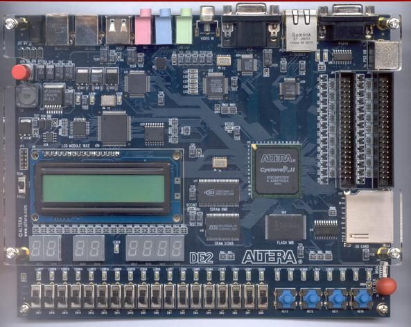
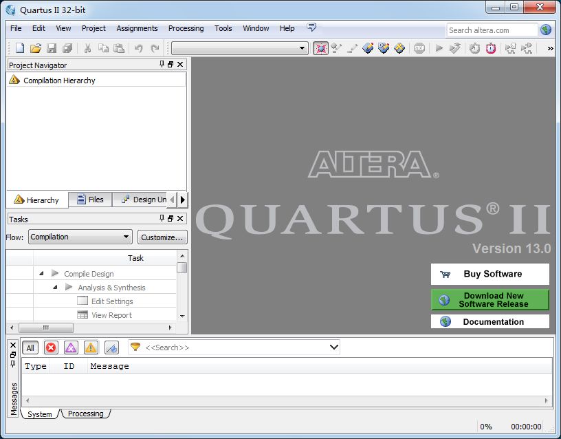
Figure 19. 32-bit Wide Color Address Mapping28 3 SYSTEM DESIGN AND BUILDING 3.1 Tools 3.1.1 Altera DE2 Development and Education Board The Altera DE2 board is the most widely used education board for learning digital logic, FPGA, and embedded system designed by Altera Corporation. It is featured with an Altera Cyclone II 2C35 FPGA. It contains I/O Interfaces, Memory, Displays, Switches, LEDs and Clocks. Figure 20 demonstrates De2 board used in this project. Figure 20. Altera DE2 Development and Education Board 3.1.2 Quartus II Design Software Quartus is a comprehensive platform for Altera FPGA design. It supports all methods of entering a description of the design into a CAD system and configured the FPGA device. Figure 21 shows the Quartus II Web Version 13.0 used in this project.
29

Figure 21. Quartus II Software Web Version 13.0

3.1.3 Qsys System Integration Tool

Qsys Tool is an updated tool from SOPC Builder which designs and implements
embedded computer systems. It allows the designer to create a digital hardware
system containing processors, memory and I/O components./9/ The component can be
chosen from the desired functional units in the graphical user interface of Quartus II
or created by the designer according to the system requirements. After the
configuration and collection of components, Qsys Tool generates the designed
hardware system automatically. Figure 22 shows the Qsys System Integration Tool.
30

Figure 22. Qsys System Integration Tool

3.2 System Hardware Design

In this project, a system based on Nios II processor was built. The system
development contains two steps: hardware design and software design. Figure 23
shows a typical development flow for the Nios II system./10/ In this chapter,
hardware design is focused on. The software design will be discussed in the next
chapter (Chapter 4). As illustrated in Figure 23, the hardware design consists of five
different steps. They are discussed in this chapter in detail.
31 Figure 23. Typical Development Flow for Nios II System 3.2.1 System Requirements Analysis Figure 24 shows the devices required in this project. DE2 board contains the Nios II system and the game application. The host PC is used to configure the hardware design and download the designed Nios II system to the DE2 board. The game is controlled by the PS/2 keyboard through the PS/2 interface and displayed on the LCD Monitor through VGA interface. From these devices, the following components are required: Nios II Processor SDRAM Controller for Memory VGA Controller IP Cores Suit PS/2 Controller IP Cores
32 Clocks for processor, SDRAM and VGA Interval Timer Figure 24. Required Devices and Collections 3.2.2 Defining and Generating the System in Qsys After the system requirement analysis, the components are needed to be chosen, specified and collected by using Qsys. The components can be chosen from the Qsys IP Cores Library shown in Figure 25 or designed by designers according the system requirements. This project contains only the predefined IP Cores provided by the Qsys System Integration Tool. No custom components are included.
33

Figure 25. Qsys IP Cores Libbrary

1) Nios II Processor Configuration

There are three types Nios II Processor in the Qsys: Nios II/e, Nios II/s, and Nios II/f.
In this project, the Nios II/e was selected as it uses the fewest logic and memory
resources and the processor parameters are set as default. Figure 26 shows the
configuration.
34

Figure 26. Configuration for Nios II Processor

2) SDRAM Controller Configuration

The DE2 board includes an 8M-Byte size SDRAM chip organized as 1M x 16 Bits x
4 Banks. Designers can access to the memory chip through the SDRAM controller IP
Cores. The necessary signals dealing with the SDRAM chip are generated by the
SDRAM controller shown in Figure 27. /11/

Figure 27. SDRAM Signals
35

There were two pages to be configured after the SDRAM Controller was selected.
Figure 28 illustrates the Memory Profile configuration and Figure 29 shows the
SDRAM Timing configuration.

Figure 28. Configuration for SDRAM Memory Profile

Figure 29. Configuration for SDRAM Timing
36

3) Clock Configuration

There are three different types of clock signal used in this system: 50MHz clock
signals for the Nios II processor and IP Cores, 25MHZ clock signal for VGA and
phase shifted 50MHz clock signal for SDRAM. The DE2 Board contains only the 50
MHz and 27 MHz clock. Thus a PLL circuit is needed for generating the three clock
signal types. This can be implemented by adding the clock signals for DE-Series
Board Peripherals IP Core. Figure 30 shows the block diagram of this clock signal IP
Core./12/ Table 8 explains the definition and description for each signal. Figure 31
shows the configuration for the clock signals for DE-Series Board Peripherals IP Core.
As there is no audio signal in this project, the output of the optional clock is only the
SDRAM and VAG clock signal.

Figure 30. Block Diagram of Clock Signal IP Core

Table 8.Clock Signals Description
    Name       Direction               Frequency(MHz)                    Description
Primary Input
                 Input                        50                      Input clock signal
    Clock
  Secondary                                                        Audio clock
                 Input                        27
 Input Clock                                                       driving clock
                                                                Core driving clock
System Clock      Output                     50
                                                                       signal
                                                                 VGA Controller
 VGA Clock        Output                     25
                                                                    clock signal
  SDRAM                                      50                 Only for SDRAM
                  Output
   Clock                             (3ns phase shifted)        chip on DE board
                                                                  Audio CODEC
Audio Clock       Output     11.2896/12.0/12.288/16.9344/18.432
                                                                 chip clock signal
37 Figure 31. Configuration for Clock IP Core As a 50 MHz clock signal was needed as the input to drive the Clock Signals for DE-series Board Peripherals IP Core, a single clock source was added to the system. Figure 32 shows the configuration for this single clock source. Clock frequency is known as 50 MHz and None for reset synchronous edges. Figure 32. Configuration for Single Clock Source
38

 4) VGA IP Cores Configuration

 In this project, the following IP Cores are used for displaying images and characters:
 Dual-Clock FIFO, Pixel Buffer DMA Controller, RGB Resampler, VGA Controller,
 Scaler, SRAM Controller, Character Buffer for VGA Display and Alpha Blender.
 There two types of image data: pixel data and character data. And they are processed
 differently by different IP Cores.

 Pixel data Processing:

 The pixel data is stored in SRAM at resolution of 320 x 240 and the color of each
 pixel is represented by 16 bits. The DMA Controller reads the pixel data from SRAM.
 Then the data is converted into 30 bits per pixel color at the resolution of 640 x 320.
 This conversion is implemented by using the Scaler and RGB Resampler. The RGB
 Resampler extends the 16-bit color in to 30-bit color. The Scaler changes the 320 x
 240 resolution into 640 x 480.

 Character data processing:

 The character data is stored in on-chip memory. The Character Buffer for VGA
 Display renders ASCII characters data into graphical format.

 After processing, both the pixel data and the character data are sent to Alpha Bender.
 The Alpha Bender then combines the two data stream into one stream and sends the
 combined data to Dual-Clock Controller. The Dual-Clock Controller sends the
 combined data stream to VGA Controller at 25MHz which is the VGA Controller
 operating frequency. Then the VGA Controller adds the data with the VGA timing
 signal and sends them to the on-board VGA DAC.

i. SRAM/SSRAM Controller Configuration

 In this project, the SRAM chip on DE2 board is used for the pixel buffer. The
 designer can access the SRAM easily through the SRAM controller by mapping the
39

 Avalon Switch Fabric signals to the chip. Figure 33 shows the configuration for
 SRAM Controller. In this project, DE2 is the target board and the SRAM is used as
 pixel buffer.

 Figure 33. Configuration for SRAM Controller

ii.Pixel Buffer DMA Controller Configuration

 The DMA Controller reads the data from the memory which is the SRAM in this
 project and sends the data out through its Avalon streaming interface. Figure 34
 shows the configuration for the DMA Controller. For this project, the consecutive
 addressing mode was selected. The default buffer start address is the SRAM address
 0x08000000 (the address is given later in this chapter) in this project. The default
 back buffer start address is the same with the default buffer start address as there is no
 back buffer in this project. According the image data stored in SRAM, the resolution
 is 320*240 and color space is 16-bit wide.
40

  Figure 34. Pixel Buffer DMA Controller Configuration

iii.Scaler Configuration

  The scaler changes the resolution of the image data stream by adding or dropping
  pixels. Figure 35 illustrates the configuration for the scaler. In this project, the scaling
  factor for width and height are both 2 as the resolution is doubled form 320 x 240 to
  640 x 480. The pixel format is 10-bit color with 3 color planes.

  Figure 35. Configuration for Scaler
41

iv. RGB Resampler Configuration

  The RGB Resampler is to convert the RGB color space. The configuration of this IP
  Core is shown in Figure 36. In this project, the incoming format is the 16-bit RGB as
  data is stored in SRAM. The out-going format is 30-bit RGB as the VGA controller
  requires.

  Figure 36. Configuration for RGB Resampler

v. Character Buffer for VGA Display Configuration

  The Character Buffer for VGA Display renders ASCII characters data into graphical
  format. The configuration for this IP Core is shown in Figure 37.
42

  Figure 37. Configuration for Character Buffer for VGA Display

vi. Alpha Blender Configuration

  The Alpha Bender combines the two data stream into one stream. Figure 38 shows the
  configuration for this IP Cores. For this project, the simple alpha blending mode was
  selected.
43

   Figure 38. Configuration for Alpha Blender

vii. Dual-Clock FIFO Configuration

   Dual-Clock FIFO contains memory for buffering the incoming data stream and
   outputs the data at a different frequency. Figure 39 shows the configuration for this IP
   Core. In this project, the color bits number is 10 and the color planes number is 3.
44

   Figure 39. Configuration for Dual-Clock FIFO

viii. VGA Controller Configuration

   Through the VGA Controller, the timing signals including HS and VS signals for the
   VGA DAC on the DE2 board are generated. The VGA controller combines the timing
   signals with the incoming data from its Avalon Streaming Interface. The combined
   data are sent to VGA DAC. Figure 40 shows the block diagram of VGA Controller.
   The configuration for VGA controller is shown in Figure 41. In this project, DE2 is
   the target board and VGA connector is the video out device. /13/

   Figure 40. Block Diagram of VGA Controller
45

Figure 41. VGA Controller Configuration

5) PS/2 Controller Configuration

PS/2 IP core supports a PS/2 mouse or keyboard collected to the board. It generates
the timing signal for communication with a device using PS/2 transmission Protocol.
Figure 42 shows the configuration for this IP Core. In this project, the Avalon type
was selected as Memory Mapped. PS/2 generates interrupts.

Figure 42. Configuration for PS/2 Controller
46

6) Interval Timer Configuration

In this project, an interval timer is used to generate interrupt. Figure 43 shows the
configuration for this IP Core. In this project, the timeout period is set as 1 ms and the
counter size is 32 bits. For the register, the readable snapshot is allowed.

Figure 43. Configuration for Interval Timer

7) Base Address and Interrupt Number Assignment

There are two ways to assign base address and interrupt numbers for the IP Cores’
register: manually or automatically by Qsys. In this project, the base address and the
nterrupt number is assigned manually as some register requires special base address.
In Figure 44, the “Base” column means the Base address and the “IRQ” column
means the interrupt number. Table 9 shows the base address and interrupt number for
each IP Core.
47

Figure 44. Base Address and Interrupt Number Assignment

Table 9.Base Address and Interrupt Number Table

         IP Core Name           Base Address(Hex) IRQ Number
       Nios II Processor           0x0a000000         -
 Pixel Buffer DMA Controller       0x10003020         -
       SRAM Controller             0x08000000         -
      SDRAM Controller             0x00000000         -
        Interval Timer             0x10002000          0
        PS/2 Controller            0x10000100          7
Character Buffer(control slave)    0x00800020         -
Character Buffer(buffer slave)     0x00802000         -

8) System Collection

The collection between the IP Cores of the system is shown in Figure 45.
48 Figure 45. System Collection
49

3.2.3 Integrate Qsys System into Quartus II Project

After the IP Cores were configured and collected, the designed Nios II system was
generated. Then the system was integrated into the project by using Quartus II. Figure
46 shows the integrated system project.

Figure 46. Integrating Nios II System to Quartus II Project

3.2.4 Pin Assignment and Hardware Design Compiling

In this project, there was no need to assign the pin manually as the pin name in the
VHDL code was defined as the same as the predefined setting file provided by Altera
Corporation. The setting file with pin assignments for DE2 is imported by Quartus II
software. After the pin assignment, the whole hardware design was compiled.
50

4 GAME DEVELOPMENT

4.1 Game Introduction

In this chapter, the development of greedy snake game is discussed. The logic of the
game is simple: Players control the snake to eat the food and get scores. The snake
becomes longer when it eats the food. If the snake hits the wall or itself, the snake is
dead and the game is over. In this design, the game has three different levels. Level-1
is the easiest. Level-2 contains some barriers. If the snake hit the barriers, the snake is
dead. Level-3 contains the barriers also, and the speed of the snake is faster.

4.2 Game Design

The game was developed using C language. The game contains two parts: Game
Menu and Game Logic. The game menu was designed for players to select the game
level. The game logic was designed for players to play the game.

4.2.1 Game Menu

The game menu is used for selecting the game level and starting the game. Figure45
shows the game menu. In Figure 47, strings representing level-1, level-2 and level-3
are displayed at fixed positions in the middle of the screen. An arrow character is
displayed for selecting different level. The arrow is initialized in the same row before
level-1 string. The position of arrow is controlled by pressing “W” and “S” key on the
PS/2 keyboard. The arrow goes up when “W” is pressed and it goes down when “S” is
pressed. The position of the arrow is limited between level-1 string and level-3 string.
The game begins when “Enter” key on the PS/2 keyboard is pressed. To find out
which key is pressed, a buffer stores the last three bytes of the data sent from the PS/2
keyboard. Then the bytes of data are checked through the Scan Code Set 2 table.
When a key is pressed, the PS/2 Controller generates an interrupt to the processor, and
the corresponding data is sent to the buffer. The flow diagram of game menu can be
51

seen in Figure 48. Figure 49 shows the flow diagram of the key controlling for game
menu.

Figure 47. Game Menu Display

Figure 48. Game Menu Flow Diagram
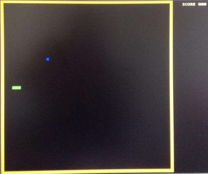
52

Figure 49. Menu Key Controlling for Selecting the Level

4.2.2 Game Logic

After the game level chosen, the game logic is executed. First, the game is initialized
and the border wall, snake and the first food are displayed on the screen. Figure 50
shows the initial image frame. The snake consists of three green pixel units. The food
is made of one blue pixel unit and the border wall is made of blue pixel units. Each
pixel unit is a 4 x 4 pixel rectangle. After the initialization, the snake waits for the
timeout signal of the interval timer. Whenever there is a timeout signal, the snake
moves one pixel unit. If the snake hits the wall or itself, the snake is dead and the
game is over. When the snake eats the food, a score is obtained and one pixel unit is
added to the snake body, making the snake longer. At the same time, new food is
generated. If the new food is generated inside of the snake body or the barriers in
level-2 and level-3, then another food is generated.

The movement of the snake is controlled by pressing “W”, “S”, “A” and “D” keys on
the PS/2 board. The game returns to game menu if the “Esc” key is pressed. The
functions of these keys are listed in table 8. As with game menu controlling, an
interrupt is generated when these keys are pressed and a buffer receives the last 3 byte
53

PS/2 data. The received data is checked to identify the pressed key. Figure 51 shows
the flow diagram of the game logic.

Figure 50. Initial Image Frame
54

Figure 51. Game Logic Flow Diagram

Table 10.Key Function for Controlling Game Logic

Key Snake Direction             Function
W         UP          Change snake moving direction
 S      Down          Change snake moving direction
 A       Left         Change snake moving direction
 D      Right         Change snake moving direction
Esc       -               Return to game menu
55

5 CONCLUSION

As a summary, the designed Nios II system was built successfully. The Greedy Snake
Game was tested by different players and it works well.

Through this project, I have benefited a lot. First, I have gained a better understanding
of the SOC and SOPC technology applied for embedded system during the Nios II
system building process. Knowledge of VGA and PS/2 has been acquired by
designing hardware for game displaying and controlling. Additionally, I improved my
programming and logic analysis skills through the game development.

As this project contains both hardware and software design for an embedded system,
it is a suitable teaching topic for students studying embedded system design. The Nios
II system is a good platform for learning FPGA and VHDL. As the DE2 FPGA board
supports RS232, Ethernet and many other interfaces, different applications based on
Nios II system can be developed. One possible topic is to develop a chess game.

Although both the Nios II system and the Greedy Snake game perform well, there are
still improvements for further study. For hardware, the PS/2 interface can be replaced
by the USB interface as the PS/2 devices are outdated. For software, the image design
can be more colorful and vivid.
56

REFERENCES

/1/ System on a Chip. Accessed March 01, 2014.
http://en.wikipedia.org/wiki/System_on_a_chip

/2/ Nios II Processor Introduction. Accessed March 01, 2014.
http://www.altera.com/devices/processor/nios2/ni2-index.html

/3/ Avalon Switch Fabric. Accessed March 03, 2014.
http://www.ee.ryerson.ca/~courses/coe718/Data-Sheets/sopc/AVALONBUS_qii54003
.pdf

/4/ VGA Timing. Accessed March 07, 2014.
http://martin.hinner.info/vga/timing.html

/5/ VGA Interface and Pinout. Accessed March 07, 2014.
http://www.allpinouts.org/index.php/VGA_15_Pin

/6/ RGB Color Model Accessed March 10, 2014.
http://en.wikipedia.org/wiki/RGB_color_model

/7/ Adam Chapweske, The PS/2 Mouse/Keyboard Protocol, 05/09/03. Accessed
March 10, 2014.
http://www.computer-engineering.org/ps2protocol/

/8/ Adam Chapweske, The PS/2 Keyboard Interface, 04/01/03. Accessed March 10,
2014.
http://www.computer-engineering.org/ps2keyboard/

/9/ About Qsys. Accessed March 14, 2014.
http://quartushelp.altera.com/13.1/master.htm#mergedProjects/system/qsys/qsys_abou
t_qsys.htm?GSA_pos=5&WT.oss_r=1&WT.oss=qsys

/10/ Nios II Hardware Development Tutorial, Altera Cooperation. Accessed March 16,
2014.
http://www.altera.com/literature/tt/tt_nios2_hardware_tutorial.pdf

/11/ Using the SDRAM on Altera’s DE2 Board with VHDL Designs, Altera
Cooperation. Accessed March 18, 2014.
ftp://ftp.altera.com/up/pub/Altera_Material/13.0/Tutorials/VHDL/DE2/Using_the_SD
RAM.pdf

/12/ Clock Signals for Altera DE-Series Board, Altera Cooperation. Accessed March
18, 2014.
57

ftp://ftp.altera.com/up/pub/Altera_Material/11.0/University_Program_IP_Cores/Alter
a_UP_Clocks.pdf

/13/ Video IP Cores for Altera DE Series Board, Altera Cooperation. Accessed March
20, 2014.
ftp://ftp.altera.com/up/pub/Altera_Material/9.1/University_Program_IP_Cores/Audio
_Video/Video.pdf
58

APPEARANCE. VHDL SAMPLE CODE

library ieee;
use ieee.std_logic_1164.all;
use ieee.std_logic_unsigned.all;

entity snake_system_top_level is

-------------------------------------------------------------------------------
--                                     Port Declarations                          --
-------------------------------------------------------------------------------
port (
     -- Inputs
     CLOCK_50                   : in std_logic;
     KEY                             : in std_logic_vector (3 downto 0);
     SW                         : in std_logic_vector (17 downto 0);

     SRAM_DQ                        : inout std_logic_vector (15 downto 0);

     DRAM_DQ                        : inout std_logic_vector (15 downto 0);

     SRAM_ADDR                      : out std_logic_vector (17 downto 0);
     SRAM_CE_N                      : out std_logic;
     SRAM_WE_N                      : out std_logic;
     SRAM_OE_N                      : out std_logic;
     SRAM_UB_N                      : out std_logic;
     SRAM_LB_N                      : out std_logic;

     DRAM_ADDR                      : out std_logic_vector (11 downto 0);
     DRAM_BA_1                      : buffer std_logic;
     DRAM_BA_0                      : buffer std_logic;
     DRAM_CAS_N                     : out std_logic;
     DRAM_RAS_N                     : out std_logic;
     DRAM_CLK                       : out std_logic;
     DRAM_CKE                       : out std_logic;
     DRAM_CS_N                      : out std_logic;
59
DRAM_WE_N : out std_logic;
DRAM_UDQM : buffer std_logic;
DRAM_LDQM : buffer std_logic;
PS2_CLK : inout std_logic;
PS2_DAT : inout std_logic;
VGA_CLK : out std_logic;
VGA_HS : out std_logic;
VGA_VS : out std_logic;
VGA_BLANK : out std_logic;
VGA_SYNC : out std_logic;
VGA_R : out std_logic_vector (9 downto 0);
VGA_G : out std_logic_vector (9 downto 0);
VGA_B : out std_logic_vector (9 downto 0);
GPIO_0 : INOUT STD_LOGIC_VECTOR(35 DOWNTO 0)
);
end snake_system_top_level;
architecture snake_system_rtl of snake_system_top_level is
component snake_system
port (
signal clk_clk : in std_logic;
-- clk.clk
signal vga_controller_external_interface_CLK : out std_logic;
-- vga_controller_external_interface.CLK
signal vga_controller_external_interface_HS : out std_logic;
-- .HS
signal vga_controller_external_interface_VS : out std_logic;
-- .VS
signal vga_controller_external_interface_BLANK : out std_logic;
-- .BLANK
signal vga_controller_external_interface_SYNC : out std_logic;
-- .SYNC
signal vga_controller_external_interface_R : out std_logic_vector(9
downto 0); -- .R
signal vga_controller_external_interface_G : out std_logic_vector(9
downto 0); -- .G
signal vga_controller_external_interface_B : out std_logic_vector(9
downto 0); -- .B60
signal sdram_clk : out std_logic;
-- sdram.clk
signal pushbuttons_external_interface_export : in std_logic_vector(3
downto 0); -- pushbuttons_external_interface.export
signal sdram_wire_addr : out
std_logic_vector(11 downto 0); --
sdram_wire.addr
signal sdram_wire_ba : out
std_logic_vector(1 downto 0);
-- .ba
signal sdram_wire_cas_n : out std_logic;
-- .cas_n
signal sdram_wire_cke : out std_logic;
-- .cke
signal sdram_wire_cs_n : out std_logic;
-- .cs_n
signal sdram_wire_dq : inout
std_logic_vector(15 downto 0); -- .dq
signal sdram_wire_dqm : out
std_logic_vector(1 downto 0);
-- .dqm
signal sdram_wire_ras_n : out std_logic;
-- .ras_n
signal sdram_wire_we_n : out std_logic;
-- .we_n
signal reset_reset_n : in std_logic;
-- reset.reset_n
signal pixel_buffer_external_interface_DQ : inout
std_logic_vector(15 downto 0); -- sram_external_interface.DQ
signal pixel_buffer_external_interface_ADDR : out
std_logic_vector(17 downto 0);
-- .ADDR
signal pixel_buffer_external_interface_LB_N : out
std_logic;
-- .LB_N
signal pixel_buffer_external_interface_UB_N : out61
std_logic;
-- .UB_N
signal pixel_buffer_external_interface_CE_N : out
std_logic;
-- .CE_N
signal pixel_buffer_external_interface_OE_N : out
std_logic;
-- .OE_N
signal pixel_buffer_external_interface_WE_N : out
std_logic;
-- .WE_N
signal ps2_external_interface_CLK : inout
std_logic;
signal ps2_external_interface_DAT : inout
std_logic;
signal joy_stick_external_interface_export : inout
std_logic_vector(31 downto 0)
);
end component;
signal BA : STD_LOGIC_VECTOR(1 DOWNTO 0);
signal DQM : STD_LOGIC_VECTOR(1 DOWNTO 0);
signal clk_25 : STD_LOGIC;
begin
DRAM_BA_1 VGA_VS,62
vga_controller_external_interface_BLANK=> VGA_BLANK,
vga_controller_external_interface_SYNC => VGA_SYNC,
vga_controller_external_interface_R => VGA_R,
vga_controller_external_interface_G => VGA_G,
vga_controller_external_interface_B => VGA_B,
sdram_clk => DRAM_CLK,
pushbuttons_external_interface_export => KEY,
sdram_wire_addr => DRAM_ADDR,
sdram_wire_ba => BA,
sdram_wire_cas_n => DRAM_CAS_N,
sdram_wire_cke => DRAM_CKE,
sdram_wire_cs_n => DRAM_CS_N,
sdram_wire_dq => DRAM_DQ,
sdram_wire_dqm => DQM,
sdram_wire_ras_n => DRAM_RAS_N,
sdram_wire_we_n => DRAM_WE_N,
reset_reset_n => KEY(0),
pixel_buffer_external_interface_DQ => SRAM_DQ,
pixel_buffer_external_interface_ADDR => SRAM_ADDR,
pixel_buffer_external_interface_LB_N => SRAM_LB_N,
pixel_buffer_external_interface_UB_N => SRAM_UB_N,
pixel_buffer_external_interface_CE_N => SRAM_CE_N,
pixel_buffer_external_interface_OE_N => SRAM_OE_N,
pixel_buffer_external_interface_WE_N => SRAM_WE_N,
ps2_external_interface_CLK => PS2_CLK,
ps2_external_interface_DAT => PS2_DAT,
joy_stick_external_interface_export(0) => GPIO_0(1),
joy_stick_external_interface_export(13 DOWNTO 1)=> GPIO_0(15
DOWNTO 3),
joy_stick_external_interface_export(14) => GPIO_0(17),
joy_stick_external_interface_export(31 DOWNTO 15)=> GPIO_0(35
DOWNTO 19)
);63 end snake_system_rtl;
You can also read