IMT-MINAFAB: a Technological Platform for integrating Education, Research and Innovation
←
→
Page content transcription
If your browser does not render page correctly, please read the page content below
IMT-MINAFAB: a Technological Platform
for integrating Education, Research and
                Innovation

    Dan Dascalu, Raluca Müller and Radu Popa

National Institute for R&D in Microtechnologies
126A, Erou Iancu Nicolae, 077190, Bucharest, Romania
Tel: +40 21 269 07 78
Fax: +40 21 269 07 72
www.imt.ro - www.imt.ro/MINAFAB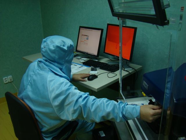
●Summary

• About IMT-MINAFAB in brief.
• Main facts, main figures.
• Major fields of research.
• Current projects.
• Equipment overview.
• Collaboration and perspectives.
The policy of the National Institute for R&D in Microtechnologies
(IMT-Bucharest) is to concentrate the operation of experimental
resources in the so-called IMT-MINAFAB (IMT Centre for MIcro-
and NAnoFABrication).

 This is done for technical reasons (the need to install and operate
many equipments in a clean room environment) and also for
organizational reasons – the need to have a concetration of
resources open for utilization of both internal and external (non IMT)
customers.
IMT operates a variety of resources, from CAD and a mask shop to
reliability testing.

Of particular importance are the equipments for nanostructuring and
characterization.

 This allows IMT to participate in various international projects,
including in nanoelectronics (such as CATHERINE from FP7 and a
couple of projects from ENIAC-JU).
The experimental facility IMT-MINAFAB is not only devoted to
partnership in research: the centre is also open to education and
industry and this opens the way for very fruitful interactions in the
so-called „knowledge triangle”

IMT will benefit from the interaction envisaged with companies
like Infinineon Technologies or Honeywell (providing services
and/or cooperating in research projects closer to the real needs
of industry),

 as well as from its involvment in educational and training
activities (providing full support for a number of four disciplines
related to the new M.Sc. courses from University „Politehnica” of
Bucharest or rulling the new IMT post doctoral programme in micro-
and nanotechnologies with 35 students).
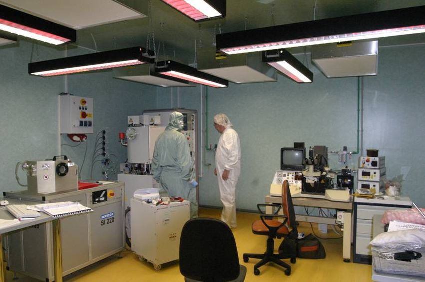
About IMT-MINAFAB,
in brief
• State of the art research infrastructure, operating since September
2008.
• Center of services for micro- and nanofabrication
• Platform of interaction as open-centre for research and education-by
research, focused on multidisciplinary innovation and knowledge
transfer to industry.
• Enables highly efficient exploitation of IMT's existing tangible and
intangible assets in nano-science/technologies (clean-room facility,
advanced equipments, knowledge and experience, partners and
clients).
• Complex technological platform: CAD tools, mask shop sector,
analysis and characterization, nano-bio-fabrication, reliability tests.
• Access is facilitated in a variety of ways, with notable accent on
developing common R&D projects and on offering direct access of
innovative companies
Main facts, main figures [1]
• Class 1000 clean room (220 sqm) for the mask shop and the most
demanding technological processes.
• Class 100,000 clean room - so called “Grey area” - (200 sqm), mostly for
the characterization equipments.
• Class 10,000 clean room (120 sqm) for thin films by CVD techniques,
RTP, etc. (to become operational).
• Accumulated total investment in equipments and infrastructure: about 9 M
Euro (2006-2009: 7 M Euro; 2008: 3.5 M, mainly from Capacities projects).

• Large range of services. Main categories:
►micro/nanofabrication for devices and systems
► inspection, analysis and characterization of surfaces, films, crystals,
nanostructures
► design, modeling and simulation
► complex RDI services - from design, to reliability testing
Main facts, main figures [2]
• Over 60 national users as partners in consortia, or based on bilateral
agreements: 30 companies, 15 research institutes, 15 universities.
• Over 30 industrial users, as partners in consortia or contracted service users:
Austria(1), Finland(1), France(1), Germany(8), Greece(1), Hungary(2),
Italy(3), Poland(1), Slovakia(2), Spain(1), Sweden(6), The Netherlands(3),
etc.
• Over 30 partners in research - FP6-7, bilateral projects: Belgium(2),
Finland(1), France(2), Germany(11), Greece(1), Hungary(1), Italy(2),
Ireland(1), Israel(1), Poland(1), Spain(1), The Netherlands(3), UK(1),
Singapore(1), etc.
• Master courses and hands-on training for students of Polytechnic
University of Bucharest

• Operation of IMT-MINAFAB conforms with best technical/technological/
management standards (e.g., degree of decontamination, safety of operation
Main facts, main figures [3]

• Accumulated funding based on:
►three projects for technological networks (2005-2008) - NanoScaleLab
and NanoBioLab, labs created in this context: nuclei of some current
experimental labs
► four infrastructure projects (2006-2008) - extension of capabilities
► eight infrastructure projects from the “Capacities” programme
(2007-2009) - five of them consolidated the “Centre of Nanotechnologies”;
reconstruction/updating of the premises.
► MIMOMEMS (FP7- REGPOT –call1) project : a Centre of Excellence in
Microwave, Millimetre Wave and Optical Devices, based on Micro-
Electro-Mechanical Systems for Advanced Communication Systems
and Sensors, in funded by the EU project No. 202897
► Various research projects in national programmes.
Main facts, main figures [4]

Results:
• IMT- MINAFAB as an integrated cluster of new experimental
laboratories initiated and operated by various research groups.
Other equipments that can be used for production (mask shop,
wafer processing etc.) are managed by execution personnel, in
a dedicated department.

 • Provides the experimental support for a number of
interdisciplinary groups, such as:
-
-Centre of Nanotechnology (CNT-IMT) under the aegis of Romanian
Academy.
-MIMOMEMS Centre of Excellence in RF and Opto MEMS( 2008-
2011) - LEA (Associated European Laboratory) “Smart MEMS”, IMT-
Bucharest in association with LAAS/CNRS, Toulouse (France) and
IESL-FORTH, Heraklion (Greece)
• Infrastructure providing state of the art services in micro-
nanotechnology and hands on education and training.
Major fields of R&D

• Collaborative multidisciplinary research, focusing on convergent micro-nano-
bio technologies, based on structuring and characterization at the nanoscale.

• Components for nanoelectronics, photonics and microwaves
- new fabrication technologies in Si, as well as in wide bandgap
semiconductors, dielectrics, polymers.
- CNT/graphene-based nanostructures for nanoelectronics (transistors and
chip interconnections).
-new concepts and structures for optical MEMS and RF-MEMS.

• Advanced nanomaterials and nanostructures for therapies, biosensing, energy
and other industries

- functionalized nanoporous materials, nanocomposite particles, microarrays.
- nanocomposite and film assemblies for fuel cells and photovoltaics.
- SAM's, immobilization and combined studies of molecular interactions.
- microfluidic components and biochips for biosensing and monitoring.
- functional films and nanocomposites for: neurosensing, constructions.
Major fields of R&D

• New technologies for fabrication and characterization

- nanolithography, mask-free nano-connections, high aspect-ratio
nanostructures.
- silicon nanoelectrodes, functional porous silicon, bio-active materials, field
emission nanostructures.
- soft-lithography and replication.
- rapid prototyping: dip-pen nanolithography, laser micromachining, 3D and
inkjet printing.
-nanomechanical characterization of materials.

IMT-MINAFAB currently provides a complex technological platform for basic
research, application-oriented R&D and even small-scale production.
.
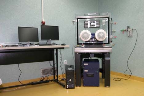
Clean room,
class 1,000
Gray Area
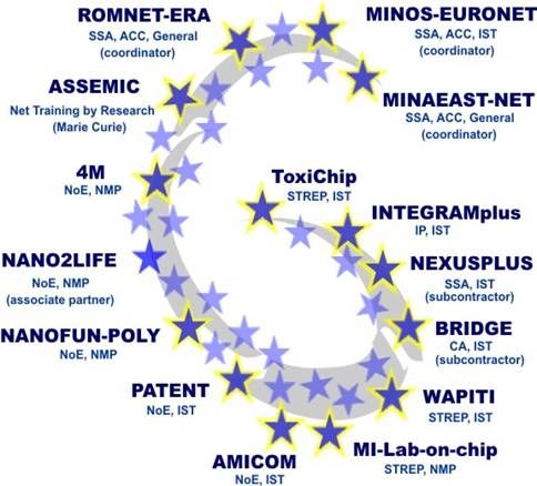
IMT- Bucharest participated in FP6 EU Projects
IMT- Bucharest
participated in
different types of EU
projects:
IPs, STREPS, NoEs,
RTN- Marie Curie
Network, SSA, CA
in ICT and NMP
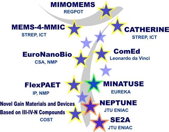
PrioritiesParticipation of IMT- Bucharest in EU FP7 (and related) projects
Participation of IMT- Bucharest in EU FP7 Projects
►European Centre of Excellence in Microwave, Millimetre Wave and
Optical Devices, based on Micro-Electro-Mechanical Systems for
Advanced Communication Systems and Sensors – MIMOMEMS, Contract
no. 202897, REGPOT call 2007-1, 2008-2011. Coordinator: IMT-Bucharest.
Contact: Dr. Alexandru Muller, (alexandru.muller@imt.ro).

►Enabling MEMS-MMIC technology for cost-effective multifunctional
RF-system integration - MEMS-4-MMIC, Contract no. 204101, STREP,
FP7-ICT-2007-2, 2008-2011. Coordinator: IMST GmbH, Germany. IMT role
Partner; IMT Contact: Dr. Dan Neculoiu, (dan.neculoiu@imt.ro).

► Carbon nAnotube Technology for High-speed nExt-geneRation nano-
InterconNEcts - CATHERINE, coord: Dr. Stephen Trueman, CONSORZIO
SAPIENZA INNOVAZIONE, Italy. Contract no. 216215, STREP, ICT, 2008-
2011. IMT role Partner; IMT Contact: Adrian Dinescu, email:
(adrian.dinescu@imt.ro).
Participation of IMT- Bucharest in EU FP7 Projects

► Flexible Patterning of Complex Micro Structures using Adaptive
Embossing Technology – FlexPAET, IP, NMP, 2008-2010. Coord: Dr.-Ing.
Christian Wenzel, Fraunhofer Gesellschaft zur Förderung der angewandten
Forschung e.V. Fraunhofer Institut für Produktionstechnolgie (IPT), Germany.
IMT role Partner; IMT Contact: Dr. Dana Cristea (dana.cristea@imt.ro);

►European scale infrastructure in NanoBiotechnology - EuroNanoBio,
CSA, NMP, 2009-2010; Coord: Patrick Boisseau CEA (France). IMT role;
partner; IMT contact: Prof. Dan Dascalu (dan.dascalu@imt.ro );

► Hazard characterization and human and environment impact
assessment of specific nanomaterials and associated products and
exploration of new solutions for their sustainable use, re-use, recycling
and final treatment and/or disposal – NANOSUSTAIN, NMP-2009-1.3-1;
ENV.2009.3.1.3.2, Project coordinator: Dr. Rudolf Reuther, NordMiljö AB,
IMT role: Partner; IMT contact Dr. Irina Kleps (irina.kleps@imt.ro).
EU projects related to FP 7

►Nanoelectronics for Safe, Fuel Efficient and Environment Friendly
Automotive Solution – SE2A; ENIAC (nanoelectronics) 2008-20111,
Coordinator: NXP Semiconductor Netherlands BV, The Netherlands. IMT
role; partner; IMT contact: Dr.Alexandru Muller (alexandru.muller@imt.ro).

►MERCURE, ENIAC (nanoelectronics), Coordinator: Thales TRT,
France; contact person: Dr.Alexandru Muller (alexandru.muller@imt.ro);
accepted Oct 2009

► Micro Nano Technology Use by SME's- MINATUSE, EUREKA, EUREKA coord:
Christophe Bruynseraede, IMEC, Belgium, 2005-2010, IMT role Partner; IMT
Contact: Eng.Ionica Miresteanu, (ionica.miresteanu@imt.ro

►Novel Gain Materials and Devices Based on III-V-N Compounds; COST
Action MP0805, Coordinator: Prof. N. Balkan, University of Essex, UK. IMT
role; partner; contact person: Dr.Alexandru Muller (alexandru.muller@imt.ro)
EU projects related to FP 7

► Development    of competences of educational staff by integrating
operational tasks into measures of vocational training and further
education" ComEd, - Leonardo da Vinci - Life Long Learning (2008-
2010) Coordinator BWAW Thüringen gGmbH, Germany, Contract Number :
DE/08/LLP-LdV/TO/147174- ( 2008-2010) IMT role Partner; IMT Contact: Dr.
Raluca Muller (raluca.muller@imt.ro)

                             ERA-NET projects
A “system-in-a-microfluidic package” approach for focused diagnostic
DNA microchips (DNASIP) Coordinator: Université Catholique de Louvain,
Belgium, Prof. Denis Flandre, role of IMT – partner, contact person: Phys.
Monica Simion (monica.simion@imt.ro).

“Nanostructural carbonaceous films for cold emitters” (NANOCAFE),
Coordinator: Industrial Institute of Electronics, Poland, Dr. Elżbieta Czerwosz,
role of IMT – partner, contact: Phys. Florea Craciunoiu
(florea.craciunoiu@imt.ro).
International partnership • Apart of cooperation with dozens of organizations from Europe in EU projects IMT- Bucharest is involved in a great number of bilateral European projects (especially with Italy, France, Belgium), • Outside Europe, IMT- Bucharest has also cooperation with organizations from: – Japan – Korea – Singapore; – South – Africa.
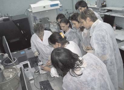
Education
¾New Master (M. Sc. Courses) at the Faculty for Electronics, Communications and
Information Technology, University “Politehnica” of Bucharest starting October 2009 and held
in IMT (with access to experimental facilities).
• Microsystems:
           - Intelligent sensors and microsystems;
           - Microphysical characterization of structures;
• Micro- and Nanoelectronics:
           - Advanced Technological Processes
• Electronic Technology for Medical Applications:
           - Micro- and Nanotechnologies for Medical Applications

¾ Postdoc program: A Postdoc program in the areas of RF MEMS and MOEMS financed
by FP7 MIMOMEMS project was launched in 2009 in IMT. Three postdocs were employed in
IMT up to now.
¾ Postdoc program Human Resource Development by Postdoctoral Research
on Micro and Nanotechnologies
¾ Other educational actions within different projects:
• FP 6: ASSEMIC - Marie Curie Training Network (2004-2007), Contract No. MRTN-CT-2003-
504826, supervising the activity of PhD students and post doc.
• 2 Leonardo da Vinci - Life Long Learning projects, where IMT was partner:
  - “Microteaching Project” (2004-2007), coordinated by RWTH Aachen University
   - “Development of competences of educational staff by integrating operational tasks into
measures of vocational training and further education" ComEd, (2008-2010) coordinated by BWAW
Thüringen gGmbH, Germany
• Short courses regarding microtechnologies were developed and presented to SMEs.
IMT-MINAFAB
View from the new clean roomReactive Ion Etching (RIE), SENTECH equipment
Working gases: CF4, CHF3, SF6, O2, Ar
RF power could be varied between 0 si 600 W,
pressure in reactor between 1 – 100 Pa, and wafers of 3 and 4 inch
Conventional and non-
conventional technological
IMT-MINAFAB
processes:
• Etching: Si, SiC, SiO2, polySi,
Si3N4, TiO2, SU8, PDMS, PMMA
• Physical-chemical reactions at
room temperature for the
modification of the surfaces
(contact angle, superficial
polymerization, hydrophilic
and/or hydrophobic surfaces).
• Plasma RF treatments for
improving the substrate
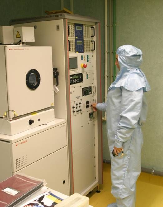
adherence.Vacuum
coating system
Processes:
IMT-MINAFAB
- DC sputtering
- e-beam
Chamber size: 500mm x 500mm
Coating materials: Al, Ni, Cr, Au,
Pt, Ti, W, etc
Up to 6 coatings in a single
vacuum process (4 e-beam, and
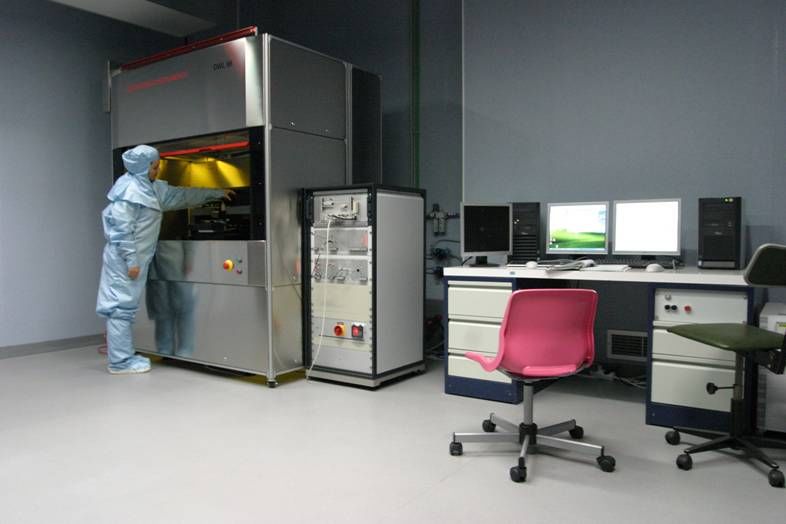
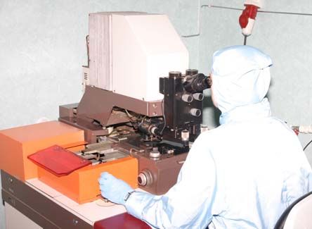
2 sputtering)Pattern generator for mask manufacturing
DWL 66fs Laser Lithography System is produced by Heidelberg
Instruments Mikrotechnik GmbH.
APPLICATIONS:
IMT-MINAFAB
-masks manufacturing for
all semiconductor
applications ( minimum
pattern : 1 µm
-direct writing (wafers,
different substrate types)
using various
photosensitive coatings
(positive and negative
resists, SU8,
photosensitive polyimide)
for all semiconductor
applications
-3D structuring in thick
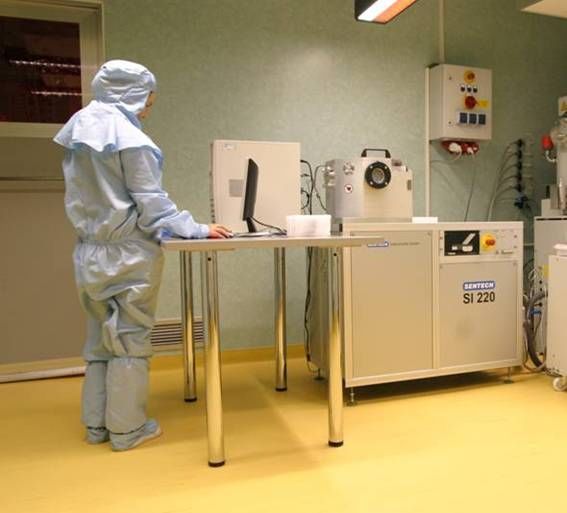
photosensitive materialsDip Pen Nanolithography system
This scanning probe lithography technique allows pattering in
nanometre range and is a direct writing method that can use
molecular and biomolecular “inks” on a variety of substrates
IMT-MINAFAB
Enables deposition
of tracks of various
materials
(polymers, sol-gel
precursors,
nanopowder,
complex molecules,
quantum dots) with
a thickness down to
30 nm.MIMOMEMS Equipments acquired in the MIMOMEMS project ► Vector Network Analyzer (VNA) up to 110 GHz and on wafer measurement facilities in order to upgrade the 0.8-65 GHz existing on wafer characterization system ► Frequency synthesiser up to 65GHz ► Au plating facility for semiconductor wafers ►White light interferometer- optical profiling system for research applications ►Near field scanning optical microscope (SNOM)
Near field scanning optical microscope (SNOM) –
        purchased in the frame of FP7 Project MIMOMEMS

                                                    Operating Modes:
                                                       Near-field microscopy: transmission,
                                                    reflection, collection, fluorescence
                                                       Confocal microscopy: transmission,
                                                    reflection, fluorescence, can be upgraded with
                                                    a Raman spectrometer
                                                       Atomic Force Microscopy contact and AC-
                                                    Mode

                                                            Applications:
                                                                - Imaging the optical properties of a
                                                            sample with resolution below the
                                                            diffraction limit with applications in
                                                            nanotechnology, nanophotonics ,
Confocal image of round   SNOM image in contact mode of     nanooptics and plasmonics
  structure 30X30 μm       an Au array of lines patterned         - Life sciences
     scanning area         using EBL – 2X2 μm scanning
                                       area                       - Materials research
                                                                  - Single molecule detection .
Field Emission Gun Scanning Electron Microscope (FEG- SEM) Nova NanoSEM 630 FEI Company, -ultra high resolution in the nanoscale range, for a variety of applications that involve sample characterization, analysis for S/TEM sample preparation Research - Materials Qualification - Surface morphology inspection - Nanometrology -Device Characterization Main current cooperation - INFN Rome CNT and graphene - FORTH Heraklion - Univ. Salerno - Univ. Kyoto
White Light Interferometer (WLI) - Photomap 3D
    Standard 2006 (FOGALE NANOTECH);

                          3D image of a 60GHz monolithically integrated
                                receiver micromachined on GaAs

                 Detail of a silicon micromachined filter
NANOSCALE LAB
High aspect ratio (12:1) structures in PMMA Diffractive Optical Element (DOE)
for photonics applications
Photonic cristals in
PMMA on silicon for near
IR applications
Mix- match litography for 300 nm fingers used
Mix-and-match lithography for biomedical applications:
for SAW devices
optical lithography (left), combined with EBL (right)
(Cooperation IMT Bucharest- IESL FORTH )NANOSCALE LAB
Structure obtained using conventional
litogrtaphy and EBID for 4 probes
measurements of electrical properties
of a polymer nanowire
(Coopertaion IMT Bucharest – UCL)
Polymer nanowire electrically
contacted using EBID
(Coopertaion IMT Bucharest – UCL)
• Nanolithography with sub 20 nm resolution;
•Three-dimensional nanostructures;
• CNT based interconnections for next-generation
integrated circuits
• CNT based nanodevices Contact Person: Phys. Adrain Dinescu
• SAW devices with nanometer interdigitated
electrodes;
• Optical devices, holograms, micro lenses, gratings
• Development of Nanodevices using E-beam induced
deposition and etching
• Development of circuits for communications based
on photonic crystalsReliability Tests - Semiconductor Characterization System (DC) with WaferProbing Station - 4200SCS/C/- - various modules- (Keithley Instruments, USA) - Mobile Thermal Airstream System - ThermoStream TP04300A- 8C3-11 (Temptronic, USA) - Damp heat Climatic chamber (Angelantoni, Italy) - Electrodynamic vibration system with thermal and electrical tests - TV 55240/LS (TIRA, Germany) - Thermal shock chamber - TSE-11-A (Espec Europe, Germany) - Universal Ovens with electrical testing - UFB 400 (Memmert, Germany) - Highly Accelerated Stress Test Chamber - temperature, humidity, pressure, polarization - EHS-211M (Espec Europe, Germany) -Free Fall Shock Machine - 0707-20 (MRAD, USA)
Modelling and Simulation Tools
● COVENTOR 2009 (modules: Architect; FlowMM; MemHenry;
MemPackage; Designer; Analyzer Std. ; MemOptics)
● MATLAB 7: Optimization Toolbox; Extended Symbolic Math
Toolbox; Partial Differential Equation Toolbox; Genetic Algorithm and
Direct Search Toolbox; Statistics Toolbox; Neural Network Toolbox;
Curve Fitting Toolbox; Spline Toolbox; Signal Processing Toolbox;
Image Processing Toolbox; Simulink
● ANSYS Multiphysics 11.0- Structural, thermal, acoustic,
electromagnetic and coupled field analyses, CFD
● COMSOL Multiphysics 3.3 and 3.4 (enabling parallel computation)
● Workstation with 4 quad-core Intel Xeon MP 2.93 GHz processors,
64 GByte RAM and 584 GByte HDD + 876 GByte external storage

► Computer aided design and simulation for passive and active
micro-photonic components using Opti-FDTD6.0 and OptiBP
► Microwave electromagnetic simulations using IE3D and
Fidelity from ZELAND software
IMT-MINAFAB full info - www.imt.ro/MINAFAB/

IMT-Bucharest - Brochure for scientific-technological services -
www.imt.ro/brosura_imt_bucuresti_2009.pdf

Quick list of capabilities and tools -
http://www.imt.ro/MINAFAB/description.htm

                 Thank you for your attention!
You can also read