Mass Transfer Technology - A Key For Micro-LED Cinemas Commercialization - 2018 QLED & Advanced Display Summit at Hollywood, June 27-28, 2018
←
→
Page content transcription
If your browser does not render page correctly, please read the page content below
Mass Transfer Technology – A Key For Micro-LED
         Cinemas Commercialization
                        Boris Kobrin, Ph.D.
                       Sr. Associate Analyst

      2018 QLED & Advanced Display Summit at Hollywood,
                      June 27-28, 2018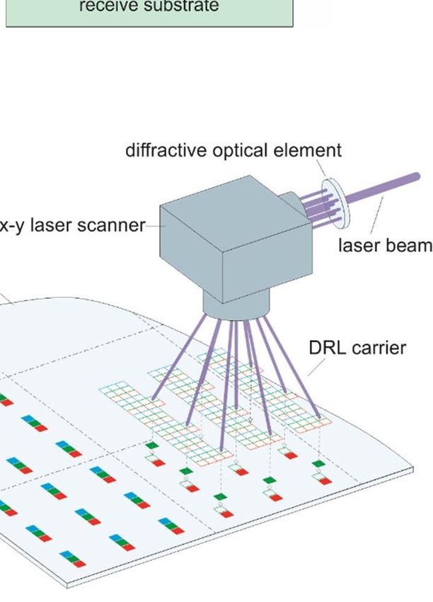
Micro-LED Presentation Information

• The information in this presentation is derived from n-tech research’s
  latest report, “Micro-LED Market Opportunities: 2018-2027.” The report
  takes a comprehensive look into the current overall marketplace for
  Micro-LED technology. This includes the technology itself, potential and
  contemporary applications, market opportunities, and many of the key
  names, both established and upcoming. The full report is available for
  purchase on n-tech’s website -

  https://www.ntechresearch.com/market-reports/microled-market/

                                                                             2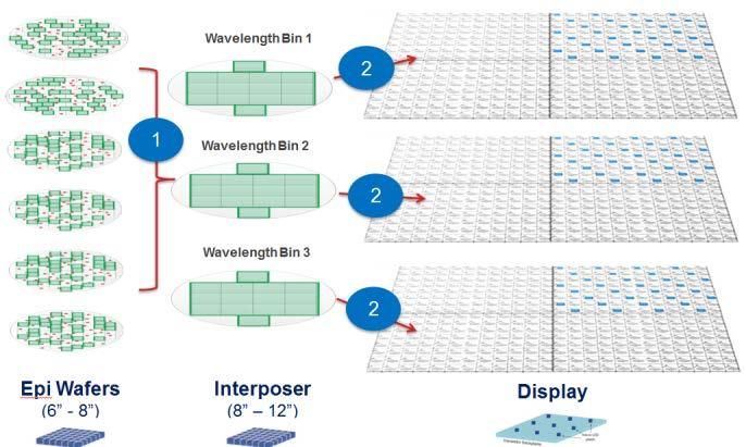
Micro-LEDs: Superior to LCD & OLED
Feature/Technology             LCD               OLED                 Micro-LED
Light source                   Backplane (LED)   Self-emissive        Self-emissive
Power consumption              High              Low (20% of LCD)     Very low (10% of LCD)
Light efficiency               Low (5-7%)        Low (5-7%)           High (~15%)
Contrast                       Medium (~5K:1)    Moderate (10K:1)     Very high (1M:1)
Response time                  Slow (ms)         Fast (us)            Very fast (ns)
Operating temperature          0-60 C            50-70 C              -100-120 C
Image retention                Low               High                 None
Color gamut                    Medium            Very good            Very good
Black level                    Medium            Very good            Very good
Brightness                     Low ( 1M nit)
Lifetime                       Medium            Short                Long
Resolution
Micro-LED Fabrication Schemes
                                                               Fully Monolithic

                               EPI                      TFT
                                             or                               Projector: AR/VR,
                               TFT                      EPI                   HUD or Smartwatch
                           TFT first              LED first
                                                              Monolithic Hybrid
                                                         EPI
                                       EPI
                                                                             Projector: AR/VR,
                                                         TFT                 HUD) or Smartwatch
                                     TFT

                                       3D integration

                                                                          Direct view:
   EPI     Mass Transfer           TFT backplane                  Smartphone, tablet, monitor, TV,
                                                                           video wall

                                                                                                     4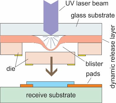
Mass Transfer of Micro-LED Dies & IC chips
B G R
IC
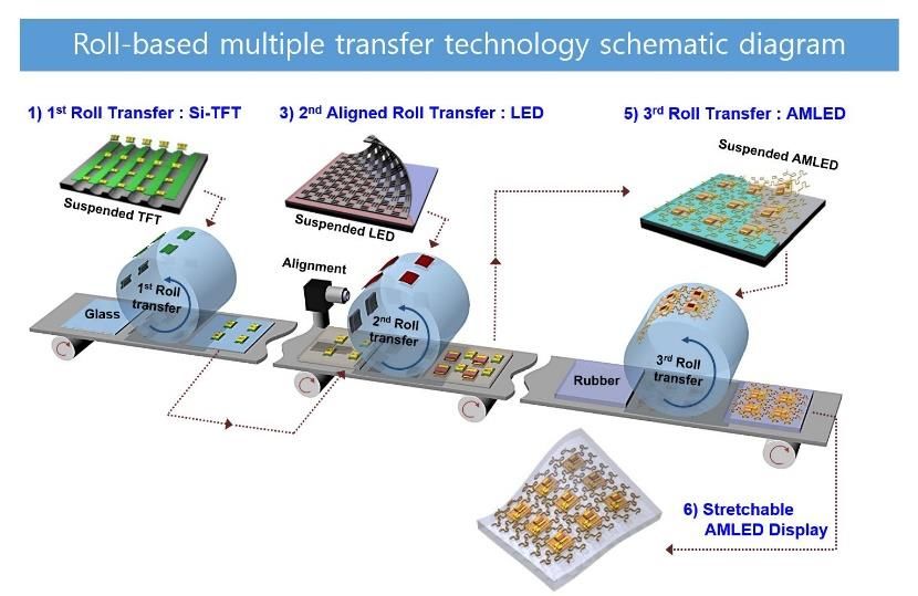
5Mass Transfer Methods
• Pick-and-place transfer (Samsung, Sony)
• Electrostatic MEMS (Apple/Luxvue)
• Electrostatic stamp (Cooledge, AUO, VueReal)
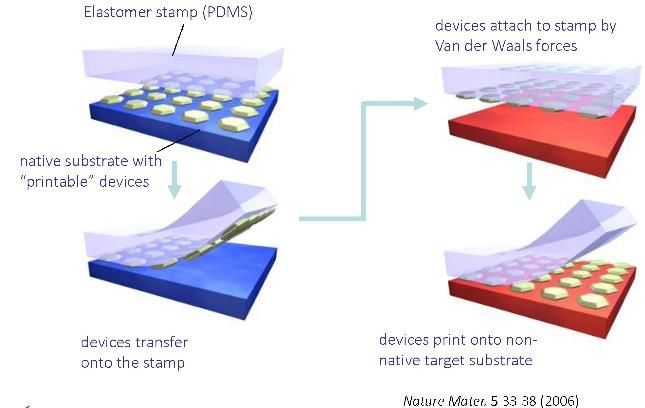
• Elastomer stamp or roll (X-Celeprint, ITRI, KIMM)
• Ultrasonic/acoustic roll (Innovasonic)
• Magnetic/electromagnetic stamp (ITRI)
• Adhesive stamp (PlayNitride, Intel)
• Mechanical transfer (Rohinni)
• Thermo-mechanical laser transfer (Uniqarta)
• Laser ablation transfer (Optivate)
• Fluidic self-assembly (Nth degree, Sharp, PSI)
6density range of 1-1000 m A /cm ,traditionalgrow th substrates can
have low efficiency due to a higher value of its non-radiative functionality of ea
recom bination param eter A . Low -dislocation G aN m aterial has non-functional de
Laser-Assisted Transfer been show n to im prove device perform ance and lim it non-
radiative recom bination under low injection conditions [2]. The
higher m anufacturi
D ue to the need fo
engineered substrate approach can thus im prove device efficiency
52-4 / V. R. Marinov
and lim it variability at the desired current density operating point
devices on a sourc
the test m ethod ca
by using high-quality G aN as a seed layer for M O C V D grow th.
not m isclassify a
Figure 4A show s a Q M A T G aN -on-Sapphire engineered substrate unacceptable level
m ade to be used as a “ print head”for m ass-transfer assem bly of electrolum inescent
m icroLE D s for displays. The grow th substrate contains num erous Photolum inescent
features that im prove dow nstream m anufacturing and m icroLED EL testing, but E
device function. possible. A m icroL
light excitation bu
injection.
Figure 2. A schematic illustrating
Uniqarta, SID 2018, 52-4 QMAT,
Figure 4: QMAT SID 2018,
E piMax™ 25-3
S ubstrate for GaN MicroLE D
Uniqarta’s laser transfer process.
Manufacturing (A= growth substrate, B= after E PI). Figure 5: Non-
Lateral Micro
The source substrate is preferably a double-side polished sapphire
substrate that can allow the individual M icroLE D s to be “
printed” Figure 5 show a po
or released onto the target display plate in a very fast m anner sub-50µm m icroLE
using a back-illum inated laser beam addressing m ethod. Figure devel
7 oped by Te
4B includes a release of a m icroLE D by a laser beam im pinging different J (A /cm 2Adhesive Stamp Mass Transfer
X-Celeprint (J. Manuf. Proc. 14, 2012 )
8Elastomeric Drum Mass Transfer
Elastomeric drum with ultrasonic actuation
Release
Ultrasonic
generator
Display substrate
Korea Institute of Machinery and Materials Innovasonic, Inc.
(KIMM)
9Figure 3b. Simulated IQE versus LED size and surface
Using Interposers (Cartridges)
recombination velocity.
entration
2
GaN LED
Veeco, SID 2018, 45-2
argets, other Figure 4. Two-step transfer approach using interposer
defectivity substrate or cartridge array.
10
ackplane.Example belowbyshows
Yield Boost that defectDies
Monochrome ratewith
can beColor
reduced by 50% by using
color conversion
Conversion solution.Dots)
(Quantum
Combined Defect Rate (ppm)
uLED Yield Transfer Yield RGB with No CC RGB with CC
(3x transfer) (1x transfer)
99.9% 99.9% 40 20
99.99% 99.99% 4 2
99.999% 99.999% 0.4 0.2
Nanosys, microLED Day, 2017
11Mass Transfer Challenges
• Narrow process window on pick up (chip on the donor should hold firmly until pick up, but
connected to it weak enough to be detached by transfer head)
• Mechanism of selecting chips (due to different density of chips on donor wafer vs display
substrate)
• Narrow process window on placement (chip on the transfer head should hold firmly
through the transfer process but be attachment should be weak enough to be detached to
display substrate). Various effects could be used to control adhesion/attachment of chips to
transfer device.
• Ultra-high transfer yield requirements - 9-9s (99.9999999%), since no dead pixel is allowed
in current display products (without redundancy).
• Throughputs requirements ~ Millions dies/s
• Very high precision of placement (within 1 µm)
• Effective (in-situ) inspection/testing methods
• Smart rework and/or sufficient redundancy scheme
12Comparison of Mass Transfer Technologies
Feature/ MEMS Mechanical Elastomeric Laser- Ultrasonic- Fluidic
Technology (pin) stamp assisted assisted self-
assembly
Reliability Moderate High Moderate High High Low
Throughput High Low Moderate High High High
Scalability Low Low High High High High
Selectivity High High Low High High Moderate
Success Low Moderate* Moderate High High Low
probability
* mini-LEDs only
13Micro-LED Display Applications Roadmap
Projection Micro-Displays Direct View Displays BLU
Near-eye HUD Automotive HUD Smart phone, TVs Video wall (>75”) LCD
Application Smart watch
projector: AR/VR projector Tablet Monitors (Forecast: Micro-LED market 2018-2027
$B
micro-LED Market (2018-2027)
80.0
70.0 $71B by 2027
60.0 CAGR ~ 65%
50.0
40.0
30.0
20.0
10.0
0.0
2018 2019 2020 2021 2022 2023 2024 2025 2026 2027
15Micro-LED Market Segmentation
Market Segmentation 2019 Market Segmentation 2025
3.7% 3.7% 0.6%
5.5% 11.5%
12.9% 15.0%
2.6% 15.3%
13.3% 5.9%
59.0% 5.6% 11.8%
4.4%
5.2%
6.2% 10.5%
3.7%
3.7%
BLU Home Theaters Digital Cinemas Digital Signage BLU Home Theaters Digital Cinemas Digital Signage
Smartwatches AR/VR Lighting TVs Smartphones Smartwatches Automotive HUD
AR/VR Lighting 3D-printers Lithography
LiFi
16Micro-LED Digital Cinema Market Forecast
Micro-LED Digital Cinema Market 2018-2027
8
7
$7B by 2027
6 CAGR ~ 60%
5
4
3
2
1
0
2018 2019 2020 2021 2022 2023 2024 2025 2026 2027
17Contact Us
facebook.com/pages/N-Tech-Research Address:
n-tech Research
PO Box 3840
twitter.com/ntechresearch Glen Allen, VA 23058
Telephone / Fax
linkedin.com/in/n-tech-research 804 938-0030
804 360 7259
Ntechresearch.com/rssfeeds Email / Web
info@ntechresearch.com
www.ntechresearch.com
18You can also read