Micro and Nano Technologies for Smart Health and personalized Medicine - Mario Baum, Nooshin Saeidi, Andreas Morschhauser, Alexander Weiss ...
←
→
Page content transcription
If your browser does not render page correctly, please read the page content below

Micro and Nano Technologies for Smart Health and
personalized Medicine

Business Unit Smart Health               October 2020

Mario Baum,
Nooshin Saeidi,
Andreas Morschhauser,
Alexander Weiss,
Christian Hedayat,
Martina Vogel,
Franziska Krause,
et.al.

© Fraunhofer ENAS
General Trends in Health and Medical Technology
Computerization:
Software and Algorithms
Artificial Intelligence for Data Evaluation
Digitization
Individualization:
Personalized Medicine
Precise drugs and treatments
Individual implants and prosthetics (3D printing)
Molecularization:
Point-of-Care diagnostics (Proteine, DNA, RNA analytics)
Organ-on-Chip
Imaging
Miniaturization:
Implants
Wearables
Nano
Mobile Health:
Remote support at home
© Fraunhofer ENAS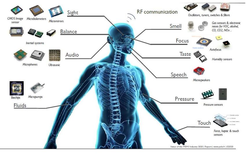
What is MEMS?
MEMS stands for Micro Electro Mechanical Systems
A technique of combining Mechanical and Electrical components
together on an chip to produce a system of miniature dimensions
dimensions less than the thickness of human hair
Why MEMS for sensors?
Smaller in size
Cheaper due to mass production
More sensitive to input variations
Have lower power consumption
Less invasive than larger devices
© Fraunhofer ENAS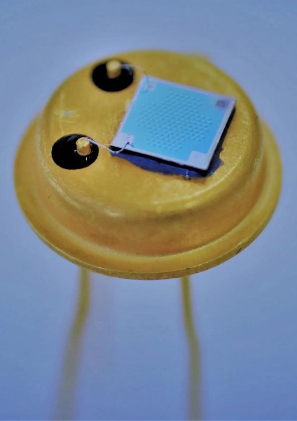
Status of MEMS for medical applications

                             Source: Yole: „Artficial Intelligence for Medical Imaging 2020“
© Fraunhofer ENAS
Business Unit at Fraunhofer ENAS
Smart Health

         Example: Highly            Example: MR-             Example: FPI MOEMS
         miniaturised implant       compatible micro         chip for optical and
         with pressure,             endoscope with           spectral analysis and
         temperature, and           Ultrasonic imaging and   micro fluidic platform
         acceleration sensor,       optical imaging, CMUT    with integrated
         ASIC, inductive link for   on an endoscope for      biosensors for DNA,
         wireless data and          therapeutic treatment    RNA, and protein
         power transfer, LTCC       of tissue.               analysis

© Fraunhofer ENAS
Innovation examples
Implants and medical equipment
High precision MEMS, highly miniaturized
and functionalized (incl. electronics)
Integration technologies for MEMS and
electronics at temperaturs below 200°C
Project reference „Endostim“
Biocompatible multi layer encapsulation
2D & 2 ranges inertial sensor Si/Glass, Ultra sonic transducer Si, Thin film encapsulation by using
Ca. 1 x 1 mm² active sensor area Ca. 6 x 6 mm²…3 x 3 mm² Parylene C, 600 nm thin
© Fraunhofer ENAS
Project example: EndoStim – CMUT on Endoscope
Introduction
Market Players Applications
CMUT market is Research • Medical Imaging
rapidly expanding. Stanford • Medical therapy
Medical imaging University, • Photoacoustic imaging
Fraunhofer, Imec,
remains the main • Gas flow sensors
University of
applications. Rome, ... • Acoustic actuator /
Industry manipulator
Hitachi, Butterfly • Non destructive
Network, Philips, testing
Kolo, Vermon
6 © Fraunhofer ENAS
CMUT - State of the Art in Medical Applications
    Dominated by medical imaging
    •    Endoscopy, Probe or Catheter based

                                                        Multi-tasking 4G CMUT linear
    Butterfly Network
                                                          matrix probe by Hitachi
    • First handheld
      CMUT probe
    • Battery operated                        M17-4                 L38-22             L30-14
    • Connected to
      smartphone

                                                      High frequency probes by Kolo

4   © Fraunhofer ENAS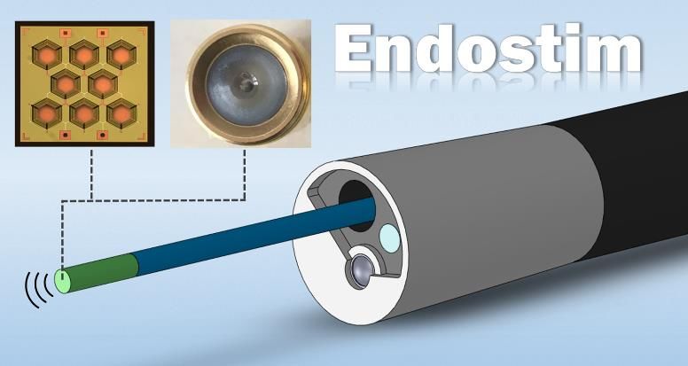
CMUT - Development Flow @ ENAS

               Material selection    Simulation    Extract device geometry

           Assembly, packaging and
                                     Fabrication   Layout & Mask design
               characterization

16 © Fraunhofer ENAS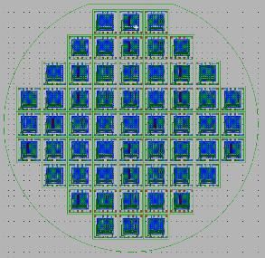
Research and Development on CMUT - Parameters

       Fabrication Technology        Wafer Bonding

       Wafer size                    6” (also possible in 8”)

       Number of die per wafer       layout and wafer size
                                     dependent (e.g. 1000)
       Number of elements per die,   Application dependent
       and CMUT cell in each die
       CMUT cell diameter            10-500µm

       Membrane thickness            Up to 10µm

       Cavity depth                  Design dependent
                                     e.g. from below 1µm to 3µm
       DC bias voltage               Up to 150V

       AC excitation voltage         Up to 150V

       Frequency range               Design dependent
                                     e.g. from below 1 MHz up to
                                     15 MHz
       Acoustic power                Design dependent
                                     Starting in kPa ranges

15 © Fraunhofer ENAS
Conclusion
High performance MEMS will generate a high potential for medical
applications, especially as a „system“
Patient specific or application specific MEMS have to fulfil cost
expectations and medical reimbursement needs! Even as a niche…
Stretchabel and flexible substrates/systems will get more and more
important for wearables even direct on skin.
Flexible electronics and sensors need smart power sources and energy
storage as well as management concepts
Encapsulation and packaging technologies will need further optimization
regarding biocompatible integration!
Research for medical products need strategic initial and preparatory
activities in close cooperation with manufacturers.
© FraunhoferThank you!
Dr.-Ing. Mario Baum
0371 / 45 001 261
mario.baum@enas.fraunhofer.de
Fraunhofer ENAS
Abteilung System Packaging
Technologie Campus 3
D-09126 Chemnitz
http://www.enas.fraunhofer.de
© FraunhoferYou can also read