Moth-eye shaped on-demand broadband and switchable perfect absorbers based on vanadium dioxide - Nature
←
→
Page content transcription
If your browser does not render page correctly, please read the page content below
www.nature.com/scientificreports

            OPEN           Moth-eye shaped on-demand
                           broadband and switchable perfect
                           absorbers based on vanadium
                           dioxide
                           Trevon Badloe1, Inki Kim1 & Junsuk Rho1,2*

                           Two biomimetic, moth-eye structure, perfect absorbers in the visible and near infrared regions are
                           introduced and investigated. The moth-eye structure is made up of vanadium oxide (VO2), which is a
                           phase change material that changes from an insulator state to a metallic state at around 85 °C. The VO2
                           structure sits on top of a sapphire (Al2O3) dielectric spacer layer, above a gold (Au) back reflector. Two
                           perfect absorbers are designed, one with perfect absorption over an ultra-broadband range between
                           400 and 1,600 nm, for both the insulating and metallic phases, while the second can switch between
                           being a perfect absorber or not in the range 1,000 and 1,600 nm. The absorption profiles and electric and
                           magnetic fields are examined and discussed to provide insight into how absorbers function in the four
                           different situations.

                           Metamaterials made of subwavelength structures that interact with light in ways that cannot be found in nature
                           have been investigated widely in recent years. In particular, absorption has been studied for various applications
                           such as, solar photovoltaics1, infrared camouflage2 and radiative cooling3. There are various designs of perfect
                           absorbers that can create either broadband or narrowband responses, each of which have their own pros and
                           cons for any given application. The materials are often structured and designed in a way to cause resonances
                           between the structures and the incoming electromagnetic field, thereby confining and absorbing it4. Techniques
                           to achieve this include using nanoantenna5,6, multilayer Fabry-Perot resonator thin films7 and nanostructured
                           metasurfaces8–11.
                               The eyes of moths are made up of an array of antireflective structures. They contain parabolic nano-hemispheres
                           with dimensions smaller than that of visible light that act as a region of graded refractive index between the
                           ambient medium and the interface. This natural feature is helpful for the moths as a mechanism to avoid any
                           unwanted reflection of light and detection from predators. Moths eyes have been studied theoretically and fab-
                           ricated experimentally to display their antireflective properties, and we previously designed an ultra-broadband
                           perfect absorber based on this shape using a range of different transition metals12. The biggest downside of cur-
                           rent metamaterials is that after a device has been designed and fabricated, it can only work in a given range or for
                           the one specific use it was designed for. To develop metamaterials into real-life, functional devices, research into
                           active metamaterials has recently started. Some examples of active metamaterials use liquid crystals to change
                           the refractive index of the surrounding medium13, flexible substrates to manipulate the resonances between
                           meta-atoms14, and phase change materials such as Ge2Sb2Te5 (GST) and Sb2S315–19 that give different responses in
                           different phases.
                               Phase change materials (PCM) have extremely useful characteristics for active nanophotonics. An external
                           stimulus such as heat, light or stress causes a PCM to change phase, from a crystalline to amorphous state, or
                           from a metallic to an insulating state, and vice versa. The switching between phases is usually fast and stable over
                           numerous changes and has the advantage of reversibility between the two states. They have been employed in
                           applications such as, radiative cooling20, data storage21,22, and even in textiles23.
                               Here, we use vanadium dioxide (VO2) as the material for moth-eye structures due to its interesting temper-
                           ature dependent phase transition between an insulator and a metal that occurs at around 85 °C. VO2 is a more
                           practical material as it is a ‘volatile’ PCM, whereas GST and Sb2S3 are ‘non-volatile’. That is to say, the phase of

                           1
                            Department of Mechanical Engineering, Pohang University of Science and Technology (POSTECH), Pohang, 37673,
                           Republic of Korea. 2Department of Chemical Engineering, Pohang University of Science and Technology (POSTECH),
                           Pohang, 37673, Republic of Korea. *email: jsrho@postech.ac.kr

Scientific Reports |   (2020) 10:4522 | https://doi.org/10.1038/s41598-020-59729-2                                                           1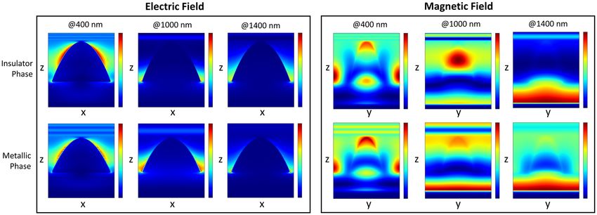
www.nature.com/scientificreports/ www.nature.com/scientificreports
Figure 1. (a) A schematic of the parabolic VO2 moth-eye structures on an Al2O3 spacer, over an Au back
reflector. (b) The measured refractive index (real (n) and imaginary (k) parts) for the metallic and insulating
phases of VO2. Solid lines represent VO2 sputtered on an Al2O3 substrate, while dashed lines represent VO2
sputtered on an Si substrate.
VO2 depends entirely on if the external stimulus is being applied or not, whereas the others state is maintained
even after the stimulus has been removed. This allows the phase of VO2 to be controlled simply by its temperature,
without having to apply some form of rapid heating or cooling to change its state.
We place the VO2 moth-eye structures on top of a sapphire (Al2O3) spacer layer, above a gold (Au) back
reflector to construct a broadband perfect absorber, a schematic is shown in Fig. 1a. By optimising the periodicity
(P) of the unit cell of a hexagonal lattice, the height (h) and the radius of curvature (c), we designed two types of
broadband perfect absorbers. The first, an ultra-broadband perfect absorber with ~99.6% absorption from 400 to
1,600 nm in both the metallic and insulator phases, and the second, a switchable broadband absorber in the near
infrared (NIR) range, that can switch between an almost perfect absorber with absorption of ~98.7%, to a poor
absorber of ~40% when switching from the metallic to insulating phase. As VO2 undergoes its phase transition
from an insulating phase at low temperatures, to a metallic phase at higher temperatures, its properties in the
visible regime are largely unchanged, whereas the imaginary part of its refractive index, i.e. absorption, at near
infrared wavelengths increases dramatically. The VO2 film samples were prepared using the sputtering method,
followed by an annealing process. This allows us to produce a very stable VO2 film that can does not oxidise
instantly. We produced samples on both a silicon (Si), and an Al2O3 substrate. Their temperature dependent
refractive index was measured with a temperature-controlled ellipsometer. The refractive index of the VO2 is
very similar regardless of substrate, owing to the sputtering method used to grow the film. This allows us to pro-
duce a VO2 film that has a consistent refractive index, regardless of the substrate or thin film it is grown on. The
measured refractive indexes are shown in Fig. 1b, and the simulations in this manuscript were performed using
the refractive index from the VO2 on an Al2O3 substrate. The phase switching properties of VO2 have been used
previously to design switchable absorbers by several other research groups, but these devices usually operate in
the THz regime24–26, or are polarisation dependent27,28. Our design operates in the ultra-broadband region from
visible to NIR (400–1,600 nm) and is largely polarisation independent. The devices designed here are suitable
for applications where the operating temperature plays a role in if we want absorption, or where the operating
temperature can be manually controlled. This near perfect absorption is essentially incident angle insensitive for
up to 60 degrees, for both TE and TM mode illumination. The influences of the metal reflector, dielectric spacer
thickness, and the working mechanisms of the broadband perfect absorbers are explored and discussed below.
Results and Discussion
2
We define the surface of the parabolic moth-eye shape by S = cr . The values c = 1/R, and r 2 = x 2 + y 2 are the
2
inverse of the radius of curvature and the position on the surface respectively. The periodicity of the hexagonal
unit cell is defined as P, while the height of the moth-eye structure is given as h and the thickness of the dielectric
spacer layer is tspacer.
Ultra-broadband perfect absorber. The first design produces an ultra-broadband perfect absorber from
400 to 1,600 nm, with a periodicity, P, of 600 nm, height, h, of 700 nm, dielectric spacer layer thickness, tspacer, of
100 nm, and radius of curvature, R, of 56 nm. At low temperatures, i.e. when the VO2 is in the insulator phase,
the moth-eye structured absorber achieves an average of 97.9% absorption across the ultra-broadband range. At
higher temperatures, when the VO2 has changed to its metal phase, the absorption increases slightly to an average
of 99.0% over the same span, as shown in Fig. 2.
The plot shows that the perfect absorber has a very similar response in the visible regime, from 400 to around
800 nm, for both phases of VO2. In this region, the refractive index and extinction coefficients of both states are
comparable. Meanwhile. in the near IR region, we can see some differences due to the metallic phase VO2 having
an increased absorption coefficient and a lower refractive index. Despite this, the designed structure still exhibits
perfect absorption over the same, ultra-broadband range. To investigate the absorption mechanisms, we plot the
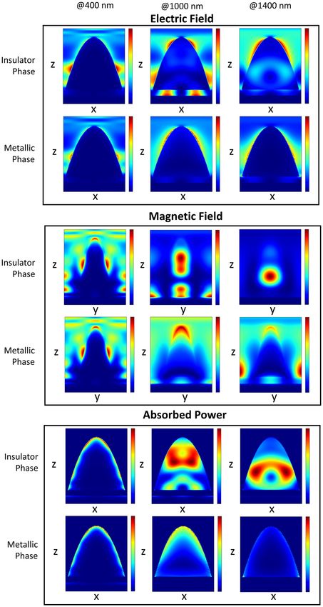
normalised calculated electric and magnetic fields, and the absorbed power distributions in Fig. 3.
Scientific Reports | (2020) 10:4522 | https://doi.org/10.1038/s41598-020-59729-2 2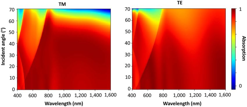
www.nature.com/scientificreports/                                                               www.nature.com/scientificreports

                           Figure 2. Absorption spectra in the metallic and insulating phases for the moth-eye structured perfect
                           absorber.

                               As we can see from the field profiles in Fig. 3, at visible wavelengths, the moth-eye absorber produces very
                           similar profiles for both phases of VO2. At 1,000 nm, the electric field for the insulating phase starts to be confined
                           in the dielectric layer between the structure and back reflector, while the magnetic field starts to form dipole res-
                           onances inside the structures. In the case of the metallic phase, the electric cannot penetrate the structure, so it is
                           confined between the structures, while the magnetic fields form resonances between the tops of the structures and
                           the back reflector, then at longer wavelengths the magnetic field gets strongly confined between the gaps in the
                           structures. We can see that in the insulating phase, at infrared wavelengths, the power is mostly absorbed inside
                           the structure in the magnetic field, which can be attributed to Mie-like resonances since the wavelength inside the
                           structures is comparable to IR wavelengths. Meanwhile in the metallic phase, the power is lost in the gaps between
                           the structures, above the dielectric spacer layer. This can be attributed to the excitation of localised surface plas-
                           mons in the small gaps. These small gaps are an indicative feature of designing moth-eye structure absorbers29,
                           as the anti-reflective performance is increased since there is less area with an abrupt refractive index change. The
                           dielectric spacer layer thickness plays no role in these mechanisms, so it has little effect on the ultra-broadband
                           absorption for this design.
                               The parabolic shape of moth-eye structures creates a gradient in the refractive index, which creates a broad-
                           band impedance matching effect30. Since the Au back reflector restricts the transmission to zero, the aforemen-
                           tioned resonances combined with the broadband impedance matching conditions that limit reflection, allow
                           for ultra-broadband absorption. In the view of fabrication, a parabolic shape is fairly difficult to achieve, so we
                           investigated four other shapes, namely a cone, square based pyramid, a circular rod, and a square rod, to see how
                           the shape of the structure affects the absorption. To do this, we used the same size shape for the base (in the case
                           of the cone and rod), while for square based structures we used a square of sides equal to the radius of the circular
                           base. The results are presented in Table 1. Since the design was optimised for the moth-eye shape, it unsurpris-
                           ingly shows the best results. The cone and pyramid shapes show fairly similar performance to the moth-eye
                           shape, especially in the metallic phase. While the linearly tapered shape of the cone and pyramid creates a form
                           of gradient in the refractive index, the magnetic field confinement inside the structure is ultimately reduced.
                           The circular and square rods have a consistent refractive index across their entire structure which inhibits their
                           broadband absorption capability in the metallic phase, as the structure does not act as an impedance matching
                           anti-reflective layer.
                               Figure 4 shows the angular dependence of the VO2 moth-eye absorber, for both TE and TM polarisation. It
                           is extremely robust to the angle of incidence with absorption over 90% for incident angles of up to 70 degrees,
                           and over 95% up to 60 degrees for both polarisations. This absorber is particularly robust for TE polarised light
                           in the IR region, and still produces peaks of perfect absorption at large incident angles for TM polarisation. The
                           slight differences at higher angles are due to the electric field rotating out of the plane of the moth eye structures,
                           thereby limiting the amount of possible confinement.

                           Switchable absorber. The second absorber that we report here has P = 200 nm, h = 200 nm, tspacer = 100 nm,
                           and R = 20 nm. This is considerably smaller than the first design and creates a switchable absorber in the near IR
                           region. By switching between the insulator and metallic phases, the average absorption from 1,000 to 1,600 nm
                           changes from a non-absorbing 38.9% to almost perfect absorption of 97.9% as shown in Fig. 5.
                               To understand why the absorption is so drastically different, we investigated the field profiles, as shown in
                           Fig. 6. The magnetic field profiles are very different to the first absorber discussed earlier in the manuscript. In
                           particular, there are no strongly confined magnetic fields inside the structures for the insulator phase, or in the
                           gaps for the metallic phase. In both cases, the magnetic field is mostly confined inside the dielectric layer at IR
                           wavelengths. At those wavelengths the size of the structures is sub-wavelength, so the same Mie-like scattering
                           cannot take place in the insulating phase, which leads to a large amount of reflection.
                               As can be seen in the background plot of Fig. 5, there is a large dip in the absorption around 800 nm. This
                           relates to a large reflectance peak that can be attributed to a Fabry-Perot cavity resonance caused by the 100 nm
                           thick spacer layer creating a metal-insulator-metal structure. This does not occur in the case of the first design,
                           since the structure is too thick. The extinction coefficient of VO2 at IR wavelengths in the insulator state is very
                           low, however it increases rapidly in the metallic state, giving rise to the high absorption in the metallic phase, but

Scientific Reports |   (2020) 10:4522 | https://doi.org/10.1038/s41598-020-59729-2                                                              3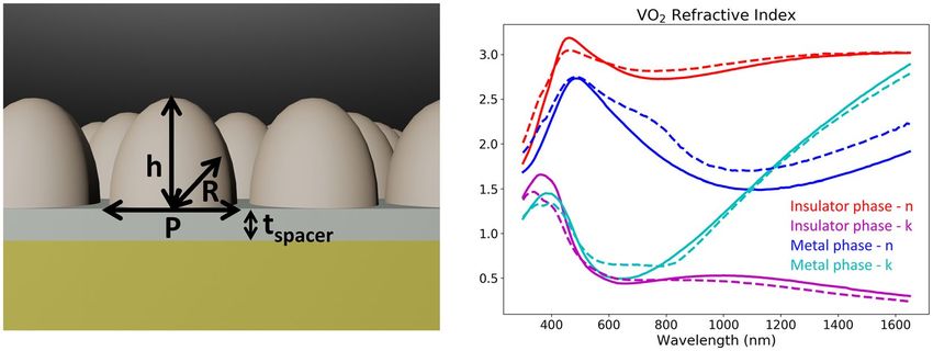
www.nature.com/scientificreports/                                                                      www.nature.com/scientificreports

                           Figure 3. The normalised field profiles for (a) the electric and (b) magnetic fields, and (c) the absorbed power
                           at selected wavelengths, chosen to represent where the fields have interesting and differing features.

                                              Moth-eye   Cone    Pyramid   Circular Rod   Square Rod
                            Insulator Phase   97.9%      89.2%   88.1%     87.7%          83.5%
                            Metal Phase       99.0%      98.8%   99.0%     84.6%          82.1%

                           Table 1. The average broadband absorption (from 400–1,600 nm) for different shaped VO2 structures on an
                           Al2O3 spacer, on top of an Au back reflector.

Scientific Reports |   (2020) 10:4522 | https://doi.org/10.1038/s41598-020-59729-2                                                            4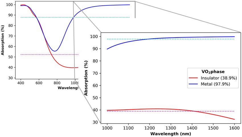
www.nature.com/scientificreports/                                                             www.nature.com/scientificreports

                           Figure 4. The angular response of the moth-eye broadband absorbers for (a) TM and (b) TE polarised incident
                           light.

                           Figure 5. The absorption profiles of the switchable absorber. At IR wavelengths the response changes from an
                           almost perfect absorber to a poorly absorbing structure as the phase changes from a metallic to insulator.

                           not in the insulator phase. We investigated the effect of the dielectric spacer layer by varying its thickness from
                           0 to 400 nm. The results are displayed in Fig. 7. With a spacer thickness of around 50 to 150 nm, we get a high
                           absorption for the metal phase as the peak of the Fabry-Perot cavity induced reflection is outside of the 1,000 to
                           1,600 nm wavelength range. As the spacer thickness increases, we get multiple reflections from the different lay-
                           ers, inhibiting the performance of the absorber. At around 100 nm, we are near the peak of the difference between
                           the metal and insulator phase absorptions while the metal phase is at a maximum, so that thickness was chosen
                           for this study.

                           Conclusions
                           Two ultra-broadband perfect absorbers made up of arrays of moth-eye structures, using VO2 have been designed
                           and investigated. The first, a perfect absorber in both insulating and metallic states from 400 nm to 1,600 nm,
                           is very robust to the incident angle for both TE and TM polarisation, with over 95% absorption up to an inci-
                           dent angle of 60 degrees. The second, a switchable absorber to non-absorber has also been proposed for wave-
                           lengths from 1,000 to 1,600 nm, utilising the interesting temperature dependent phase shift in VO2. The working
                           mechanism is attributed to a combination of the antireflective nature of the nanostructures due to the broad-
                           band impedance matching created by the tapered shape of a parabolic moth-eye type structure, combined with
                           the excitation of localised surface plasmons in the metallic phase and strong confinement of magnetic field by
                           Mie-like resonances in the dielectric case. The Au back reflector should be thick enough (over ~30 nm) to block
                           all transmitted light. While a dielectric spacer thickness of around 100 nm was found to be optimal to allow for
                           ultra-broadband absorption and switchable absorption, with variations in the thickness having negligible impact.
                           The shape of the structure does not necessarily need to be a parabola, although it shows the best performance,

Scientific Reports |   (2020) 10:4522 | https://doi.org/10.1038/s41598-020-59729-2                                                          5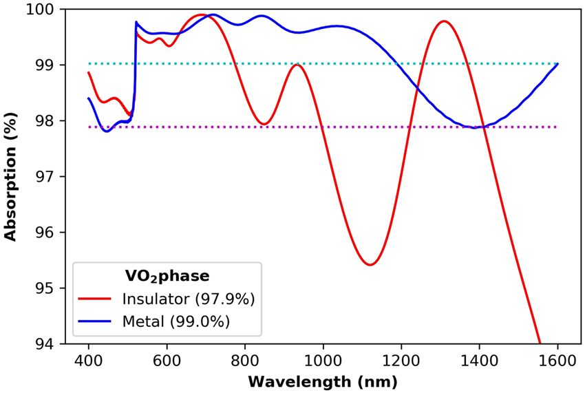
www.nature.com/scientificreports/                                                              www.nature.com/scientificreports

                           Figure 6. The field profiles for (a) the electric and (b) magnetic fields at selected wavelengths.

                           Figure 7. Al2O3 spacer layer thickness dependence on the absorption for the switchable absorber.

                           since simpler to fabricate structures such as cones and pyramids show comparable ultra-broadband perfect or
                           switchable absorption.
                               The transition temperature of VO2 depends on the growth conditions and composition. Here our VO2 sample
                           had a switching temperature of 85 °C, whereas different temperatures of the phase change have been reported
                           elsewhere. This critical temperature could be controlled and lowered to more reasonable, everyday temperatures
                           by doping with other materials31,32. This could open up possibilities of active temperature dependent absorbers or
                           tunable color filter33,34, for uses such as in smart windows or solar cells at usable daily temperatures.
                               Although the device is not fabricated in this paper, it is expected that the device could be realised effectively
                           through the nanoimprint method, or even with general electron beam lithography and the corresponding etching
                           processes.

                           Methods
                           The simulations were all performed using the commercially available FDTD solver, Lumerical FDTD solutions.
                           Monitors were placed in the substrate, and behind the source to measure the transmitted and reflected responses
                           respectively. Then the absorption was calculated as A = 1 − T − R, with care taken with regards to the sign of the
                           response of the monitor, since the recorded response is negative from the transmission monitor. Anti-symmetric
                           boundary conditions were used on the x-axis, with symmetric boundary conditions on the y-axis due to the
                           symmetry of the design for TM polarised incident light (and vice versa for TE) to help speed up simulations.
                           Boundary conditions on the z-axis were set to perfectly matched layers (PML). The mesh around the structures
                           was set to 1 nm cells in the x, y and z directions and thorough convergence testing was performed to be sure that
                           the small gaps between the nanostructures did not cause any problems.

                           Data availability
                           All data generated or analysed during this study is included in this published article.

                           Received: 25 November 2019; Accepted: 29 January 2020;
                           Published: xx xx xxxx

Scientific Reports |   (2020) 10:4522 | https://doi.org/10.1038/s41598-020-59729-2                                                            6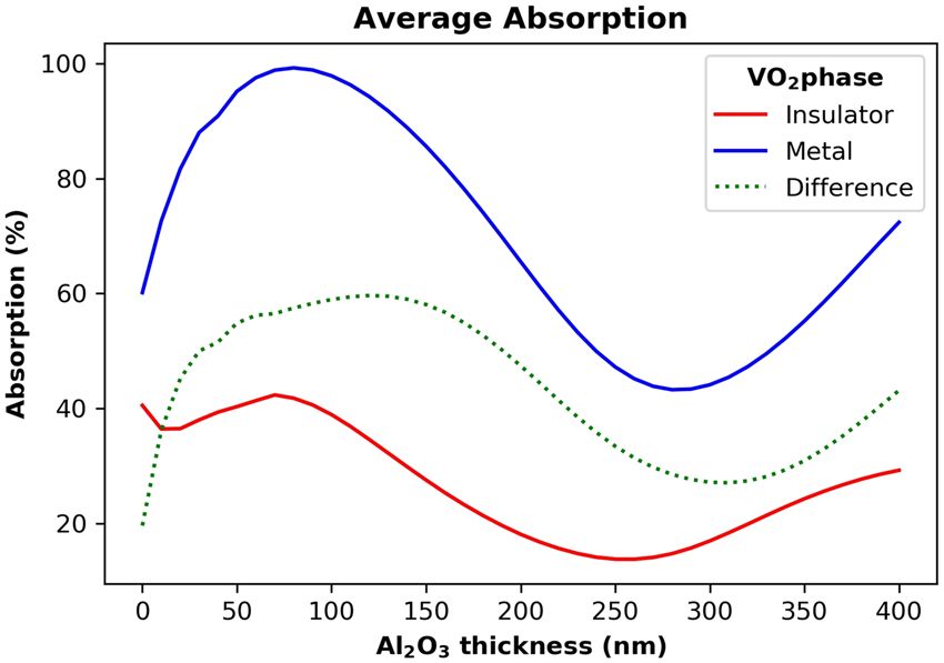
www.nature.com/scientificreports/                                                                           www.nature.com/scientificreports

                           References
                            1. Azad, A. K. et al. Metasurface Broadband Solar Absorber. Sci. Rep. 6, 20347 (2016).
                            2. Chandra, S., Franklin, D., Cozart, J., Safaei, A. & Chanda, D. Adaptive Multispectral Infrared Camouflage. ACS Photonics, 5
                               (11), 4513–4519 (2018).
                            3. Ko, B. Lee, D., Badloe, T. & Rho, J. Metamaterial-based radiative cooling: Towards energy-free all-day cooling. Energies, 12(1), 89
                               (2019).
                            4. Badloe, T., Mun, J. & Rho, J. Metasurfaces-Based Absorption and Reflection Control: Perfect Absorbers and Reflectors. J.
                               Nanomater. 2017, 1–18 (2017).
                            5. Rana, A. S., Mehmood, M. Q., Jeong, H., Kim, I. & Rho, J. Tungsten-based Ultrathin Absorber for Visible Regime. Sci. Rep. 8, 2443
                               (2018).
                            6. Kim, I., So, S., Rana, A. S., Mehmood, M. Q. & Rho, J. Thermally robust ring-shaped chromium perfect absorber of visible light.
                               Nanophotonics 7, 1827–1833 (2018).
                            7. Li, Z., Butun, S. & Aydin, K. Large-Area, Lithography-Free Super Absorbers and Color Filters at Visible Frequencies Using Ultrathin
                               Metallic Films. ACS Photonics 2, 183–188 (2015).
                            8. Cui, Y. et al. Plasmonic and metamaterial structures as electromagnetic absorbers: Plasmonic and metamaterial absorbers. Laser
                               Photonics Rev. 8, 495–520 (2014).
                            9. Li, W. et al. Circularly polarized light detection with hot electrons in chiral plasmonic metamaterials. Nat. Commun. 6, 8379 (2015).
                           10. Wang, Z. et al. Circular Dichroism Metamirrors with Near-Perfect Extinction. ACS Photonics 3, 2096–2101 (2016).
                           11. Kang, L. et al. Preserving Spin States upon Reflection: Linear and Nonlinear Responses of a Chiral Meta-Mirror. Nano Lett. 17,
                               7102–7109 (2017).
                           12. Badloe, T., Kim, I. & Rho, J. Biomimetic ultra-broadband perfect absorbers optimised with reinforcement learning. Phys. Chem.
                               Chem. Phys. 22, 2337–2342 (2020).
                           13. Franklin, D., Frank, R., Wu, S.-T. & Chanda, D. Actively addressed single pixel full-colour plasmonic display. Nat. Commun. 8, 15209
                               (2017).
                           14. Tseng, M. L. et al. Two-Dimensional Active Tuning of an Aluminum Plasmonic Array for Full-Spectrum Response. Nano Lett. 17,
                               6034–6039 (2017).
                           15. Gholipour, B., Zhang, J., MacDonald, K. F., Hewak, D. W. & Zheludev, N. I. An All-Optical, Non-volatile, Bidirectional, Phase-
                               Change Meta-Switch. Adv. Mater. 25, 3050–3054 (2013).
                           16. Yin, X. et al. Active Chiral Plasmonics. Nano Lett. 15, 4255–4260 (2015).
                           17. Tittl, A. et al. A Switchable Mid-Infrared Plasmonic Perfect Absorber with Multispectral Thermal Imaging Capability. Adv. Mater.
                               27, 4597–4603 (2015).
                           18. Qu, Y., Li, Q., Cai, L. & Qiu, M. Polarization switching of thermal emissions based on plasmonic structures incorporating phase-
                               changing material Ge 2. Sb. 2 Te 5. Opt. Mater. Express 8, 2312 (2018).
                           19. Dong, W. et al. Wide Bandgap Phase Change Material Tuned Visible Photonics. Adv. Funct. Mater. 29, 1806181 (2019).
                           20. Ono, M., Chen, K., Li, W. & Fan, S. Self-adaptive radiative cooling based on phase change materials. Opt. Express 26, A777 (2018).
                           21. Ielmini, D. & Lacaita, A. L. Phase change materials in non-volatile storage. Mater. Today 14, 600–607 (2011).
                           22. Raeis-Hosseini, N. & Rho, J. Dual-Functional Nanoscale Devices Using Phase-Change Materials: A Reconfigurable Perfect Absorber
                               with Nonvolatile Resistance-Change Memory Characteristics. Appl. Sci. 9, 564 (2019).
                           23. Gao, T. et al. Three-Dimensional Printed Thermal Regulation Textiles. ACS Nano 11, 11513–11520 (2017).
                           24. Zhao, Y., Huang, Q., Cai, H., Lin, X. & Lu, Y. A broadband and switchable VO2-based perfect absorber at the THz frequency. Opt.
                               Commun. 426, 443–449 (2018).
                           25. Liu, Z. et al. Design and fabrication of a tunable infrared metamaterial absorber based on VO2 films. J. Phys. D Appl. Phys. 50, 385104
                               (2017).
                           26. Liu, Z. et al. Dynamic infrared thin-film absorbers with tunable absorption level based on VO2 phase transition. Opt. Mater. Express
                               8, 2151 (2018).
                           27. Kocer, H. et al. Intensity tunable infrared broadband absorbers based on VO2 phase transition using planar layered thin films. Sci.
                               Rep. 5, 13384 (2015).
                           28. Lei, L. et al. Tunable and scalable broadband metamaterial absorber involving VO2 -based phase transition. Photonics Res. 7, 734
                               (2019).
                           29. Weiblen, R. J. et al. Optimized moth-eye anti-reflective structures for As_2S_3 chalcogenide optical fibers. Opt. Express 24, 10172
                               (2016).
                           30. Contractor, R., D’Aguanno, G. & Menyuk, C. Ultra-broadband, polarization-independent, wide-angle absorption in impedance-
                               matched metamaterials with anti-reflective moth-eye surfaces. Opt. Express 26, 24031 (2018).
                           31. Kim, H., Charipar, N. A., Figueroa, J., Bingham, N. S. & Piqué, A. Control of metal-insulator transition temperature in VO2 thin
                               films grown on RuO2 /TiO2 templates by strain modification. AIP Adv. 9, 015302 (2019).
                           32. Huang, T. et al. Metal-insulator phase transition in Hf-doped VO2 (M) thin films: a study on the structural, electrical, optical and
                               infrared radiation properties. Opt. Mater. Express 8, 2300 (2018).
                           33. Shu, F.-Z. et al. Dynamic plasmonic color generation based on phase transition of vanadium dioxide. Adv. Opt. Mater. 6, 1700939
                               (2018).
                           34. Lee, T., Jang, J., Jeong, H. & Rho, J. Plasmonic-and dielectric-based structural coloring: from fundamentals to practical applications.
                               Nano Converg. 5, 1 (2018).

                           Acknowledgements
                           This work was supported by the Green Science program funded by POSCO, and the National Research Foundation
                           (NRF) grants (NRF-2019R1A2C3003129, CAMM-2019M3A6B3030637, NRF-2019R1A5A8080290, NRF-
                           2018M3D1A1058997) funded by the Ministry of Science and ICT (MSIT) of the Korean government. I.K.
                           acknowledges the Global Ph.D. Fellowship (NRF-2016H1A2A1906519) by NRF-MSIT of the Korean government.

                           Author contributions
                           J.R., T.B. and I.K. conceived the concept. T.B. performed the simulations and wrote the manuscript. T.B. and I.K.
                           analysed the data. J.R. guided the entire work. All authors read and approved the final manuscript.

                           Competing interests
                           The authors declare no competing interests.

                           Additional information
                           Correspondence and requests for materials should be addressed to J.R.

Scientific Reports |   (2020) 10:4522 | https://doi.org/10.1038/s41598-020-59729-2                                                                                  7
www.nature.com/scientificreports/ www.nature.com/scientificreports
Reprints and permissions information is available at www.nature.com/reprints.
Publisher’s note Springer Nature remains neutral with regard to jurisdictional claims in published maps and
institutional affiliations.
Open Access This article is licensed under a Creative Commons Attribution 4.0 International
License, which permits use, sharing, adaptation, distribution and reproduction in any medium or
format, as long as you give appropriate credit to the original author(s) and the source, provide a link to the Cre-
ative Commons license, and indicate if changes were made. The images or other third party material in this
article are included in the article’s Creative Commons license, unless indicated otherwise in a credit line to the
material. If material is not included in the article’s Creative Commons license and your intended use is not per-
mitted by statutory regulation or exceeds the permitted use, you will need to obtain permission directly from the
copyright holder. To view a copy of this license, visit http://creativecommons.org/licenses/by/4.0/.
© The Author(s) 2020
Scientific Reports | (2020) 10:4522 | https://doi.org/10.1038/s41598-020-59729-2 8You can also read