Nanoscale Advances - The Royal Society of ...
←
→
Page content transcription
If your browser does not render page correctly, please read the page content below
Volume 3
                                                                                         Number 15
                                                                                         7 August 2021

Nanoscale
                                                                                         Pages 4295–4614

Advances
rsc.li/nanoscale-advances

                            ISSN 2516-0230

                            PAPER
                            Junfeng Gao, Yan Su et al.
                            Robust charge spatial separation and linearly tunable band
                            gap of low-energy tube-edge phosphorene nanoribbon
Nanoscale
Advances
This article is licensed under a Creative Commons Attribution-NonCommercial 3.0 Unported Licence.
View Article Online
PAPER View Journal | View Issue
Robust charge spatial separation and linearly
Cite this: Nanoscale Adv., 2021, 3, 4416
tunable band gap of low-energy tube-edge
Open Access Article. Published on 31 May 2021. Downloaded on 10/7/2021 10:47:50 PM.
phosphorene nanoribbon†
Mingyue Xia,a Hongsheng Liu, a
Lu Wang, b
ShiQi Li,a Junfeng Gao, *a
Yan Su *a and Jijun Zhaoa
Versatile applications have been proposed for phosphorene nanoribbons (PNRs), whose properties depend
strongly on the edge structures. Recently, a unique tube-reconstruction at the zigzag edge (ZZ[Tube]) of
PNRs was discovered to be the lowest configuration. Therefore, studies on PNRs should be
reconsidered. In this paper, we systemically explore the width and strain effects on zigzag PNRs with
different edge structures, including ZZ[Tube], ZZ and ZZ[ad] edges. ZZ PNRs always have small band
gaps which are nearly independent of both width and strain. A remarkable band gap exists in ZZ[ad]
PNRs which increases with a decrease in the ribbon width but is not sensitive to strain. In contrast, the
band gaps of ZZ[Tube] PNRs change from 1.08 to 0.70 eV as the width increases from 12 to 65 Å. In
addition, the band gaps of ZZ[Tube] PNRs show a linear response under a certain range of strain. In
addition, the carrier effective masses (0.50 m0 for electrons and 0.94 m0 for holes) of ZZ[Tube] PNRs are
Received 6th May 2021
Accepted 29th May 2021
much lower than for ZZ[ad], and the VBM and CBM charges are robustly spatially separated even under
strains ranging from 5% to 5%. Their ease of formation, lowest energy, light effective mass, linear band
DOI: 10.1039/d1na00332a
gap response to strain and robust charge spatial separation provide ZZ[Tube] PNRs with potentially
rsc.li/nanoscale-advances excellent performance in microelectronic and opto-electric applications.
shuttle-shaped edge bands,25 and highly efficient solar cell by edge
Introduction modications.26
Phosphorene not only has high carrier mobilities,1 but also has However, a remarkable edge state is likely to be passivated
a suitable band gap with a high on/off switching ratio (102 to by edge reconstruction. For example, a graphene zigzag (ZZ)
105).1–8 It lls in the gap between graphene (very high mobility and edge can easily form 5j7 reconstructions,27–31 and MoS2 ZZ
low on/off ratio) and transition metal dichalcogenides (low edges undergo special (2 1) and (3 1) reconstructions.32
mobility and very high on/off ratio).9–12 In addition, phosphorene Early theoretical calculations showed that pristine ZZ phos-
has strongly anisotropic behavior.2,13–17 As a consequence, phos- phorene nanoribbons (PNRs) are metallic.33,34 However, scan-
phorene is proposed as a superior candidate for future fast ning tunneling microscopy (STM) suggests that ZZ PNRs are
nanoelectronic devices. semiconductors with a remarkable band gap,35 indicating that
The two most important factors are edge and width for nano- an edge reconstruction may exist. A relaxed pristine zigzag
ribbons, which are common structures for 2D material applica- edge with a charge density wave (CDW) (called the ZZ-edge
tions.18–21 Firstly, the properties of nanoribbons depend strongly on here) is semiconducting, but its band gap is only 0.1 eV, or
edge structures, which may possess remarkable edge states.22,23 even smaller.36 A Klein-edge with a (2 1) reconstruction
Indeed, versatile applications based on the properties of phos- (named the ZZ[ad]-edge in this paper) was later proposed to be
phorene nanoribbon edges have been predicted, such as topo- more stable, but its edge state is above the Fermi level, unlike
logical edge states accommodated in the quasi-at band,24 unique the experimental nding where the edge state is below Fermi
level.31,36
Previously, there was an attempt to assemble a 1D carbon
a
Key Laboratory of Material Modication by Laser, Ion and Electron Beams (Dalian nanotube with graphene nanoribbon to introduce van Hove
University of Technology), Ministry of Education, Dalian, 116024, China. E-mail: singularities.37 Interestingly, the zigzag edge of black phosphorene
gaojf@dlut.edu.cn; su.yan@dlut.edu.cn can self-reconstruct into an ultimate narrow phosphorene nano-
b
Institute of Functional Nano & So Materials (FUNSOM), Jiangsu Key Laboratory for tube, spontaneously assembling a 1D phosphorene nanotube with
Carbon-Based Functional Materials & Devices, Soochow University, Suzhou, Jiangsu
nanoribbon.36 It was found that such a tubed edge is the lowest edge
215123, China
† Electronic supplementary information (ESI) available. See DOI:
conguration. In addition, a ZZ[Tube] PNR with 4 nm width has
10.1039/d1na00332a a remarkable band gap of 1.23 eV, and the edge state is below the
4416 | Nanoscale Adv., 2021, 3, 4416–4423 © 2021 The Author(s). Published by the Royal Society of Chemistry
View Article Online
Paper Nanoscale Advances
Fermi level, agreeing with the experiments very well.35,36 Further decrease with increasing strain. Therefore, we can infer that
studies indicate that the tube-reconstruction can also change the width and strain certainly affect the properties of reconstructed
thermal vibration and thermal transport of PNRs.38–42 Therefore, ZZ ZZ[Tube] PNRs. However, to the best of our knowledge, the
[Tube] certainly remarkably alters the properties of the PNR, and the width and strain effects on the ZZ[Tube] PNRs have not been
This article is licensed under a Creative Commons Attribution-NonCommercial 3.0 Unported Licence.
proposed applications based on the tube edge should be further studied, which is signicant for applications.
explored. In this paper, using density functional theory (DFT) calcu-
A second important factor is that the properties of nano- lations, we compare the effects of ribbon width and strain on
ribbons vary with width due to the quantum connement effect. the electronic properties of PNRs, including ZZ, ZZ[ad] and ZZ
For example, the band gap of armchair graphene nanoribbons [Tube]. Our results show that the behaviors of ZZ[Tube] PNRs
follows a 3p + 2 rule.27,43 MoS2 nanoribbons44 and armchair h- are very different from those of ZZ and ZZ[ad] PNRs. The band
BN nanoribbons45 also exhibit oscillating band gaps with gap of ZZ[Tube] PNRs can be effectively tuned by both width and
Open Access Article. Published on 31 May 2021. Downloaded on 10/7/2021 10:47:50 PM.
a variation in ribbon width. In addition, the band gap of sem- strain. In addition, ZZ[Tube] PNRs exhibit unique and robust
iconducting graphene nanoribbons46 decreases monotonically charge spatial separation of the valence band maximum (VBM)
with an increase in the ribbon width. In addition to the edge and conduction band minimum (CBM) under 5% to 4%
state and width, strain engineering is also an effective method strain. Robust spatial charge separation and the tunable band
of tuning the properties of nanoribbons.41,47 The band gaps of gap of ZZ[Tube] PNRs suggest their potential applications in
armchair MoS2 (ref. 48) and zigzag h-BN49 nanoribbons microelectronics and opto-electronics.
Fig. 1 The geometries of zigzag PNRs with different edge structures (a–c) and the band structures of PNRs with a width of 40 Å (d–f) and with
a width of 15 Å (g–i). The highest valance band and lowest conductive band are labeled in red and blue, respectively. The charge contributions to
VBM and CBM are presented beside each band structure with an isosurface value of 1.2 104 jej bohr3.
© 2021 The Author(s). Published by the Royal Society of Chemistry Nanoscale Adv., 2021, 3, 4416–4423 | 4417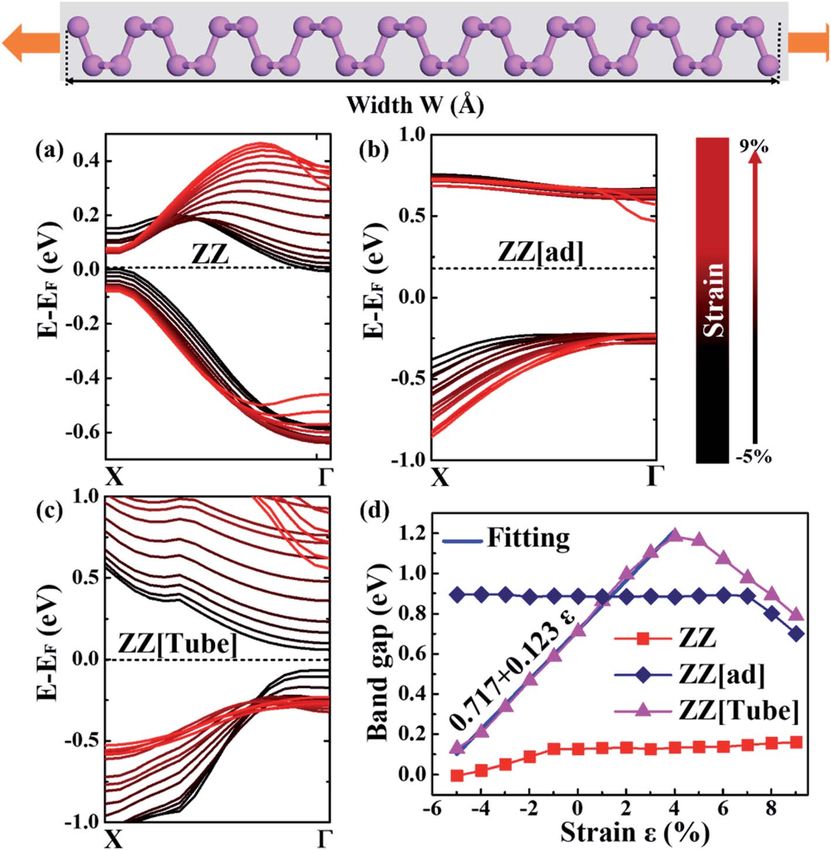
View Article Online
Nanoscale Advances Paper
Results and discussion structures, which can be understood via the charge of the
valence band maximum (VBM) and the conduction band
Our calculations50,51 were carried out with the Vienna Ab-initio bottom (CBM) shown in Fig. 1d–f. For ZZ PNR, both VBM and
Simulation Package (VASP), using the planewave basis with CBM are contributed by edge states. For ZZ[ad] PNR, the VBM is
This article is licensed under a Creative Commons Attribution-NonCommercial 3.0 Unported Licence.
a carefully tested energy cutoff of 460 eV. Details of the mainly contributed by bulk states and the CBM is contributed
computational method can be found in the ESI.† ZZ[Tube] is the by edge states. In contrast, for ZZ[Tube] PNR, the VBM is
lowest edge,35,36 while ZZ and ZZ[ad] were the most explored. contributed by edge states and the CBM is contributed by bulk
Therefore, here only PNRs with ZZ, ZZ[ad] and ZZ[Tube] edges states.
are compared, as shown in Fig. 1a–c. For each kind of PNR, the In addition, the carrier effective masses at the CBM and VBM
ribbon can be either symmetric or asymmetric, depending on of ZZ[Tube] PNR (0.42 m0 for electrons and 1.24 m0 for holes) are
the orientation of the two edges. We nd the properties of PNRs much smaller than for ZZ[ad] PNR (9.06 m0 for electrons and
Open Access Article. Published on 31 May 2021. Downloaded on 10/7/2021 10:47:50 PM.
are nearly independent of the orientation of the edge; therefore 8.80 m0 for holes) due to the larger dispersion of the bands.
for simplicity only the results with asymmetric edges are pre- Therefore, a large carrier mobility can be expected in ZZ[Tube]
sented in the manuscript. All the results for PNRs with PNR, which is important for applications in electronic devices.
symmetric edges can be found in Fig. S1–S4 in the ESI.† ZZ PNR has comparable carrier effective masses (0.50 m0 for
The band structures for ZZ, ZZ[ad] and ZZ[Tube] PNRs with electrons and 0.94 m0 for holes) to those of ZZ[Tube] PNR but it
40 Å width are shown in Fig. 1d–f. All three PNRs are semi- is much less stable. Therefore, edge reconstruction can signif-
conductors with band gaps of 0.13, 0.88 and 0.73 eV for ZZ, ZZ icantly alter the nature of the electronic structure.
[ad] and ZZ[Tube], respectively. These agree well with previous We further roughly checked the width effect by comparing
research.35,36 However, essential differences exist in the band calculations of the electronic structures of PNRs with
Fig. 2 The changes in VBM and CBM with ribbon width for ZZ, ZZ[ad] and ZZ[Tube] PNRs (a–c). The horizontal dashed lines indicate the Fermi
level. The band gaps of ZZ, ZZ[ad] and ZZ[Tube] PNRs are a function of ribbon width (d). At the top, a schematic diagram is presented showing the
definition of the ribbon width.
4418 | Nanoscale Adv., 2021, 3, 4416–4423 © 2021 The Author(s). Published by the Royal Society of Chemistry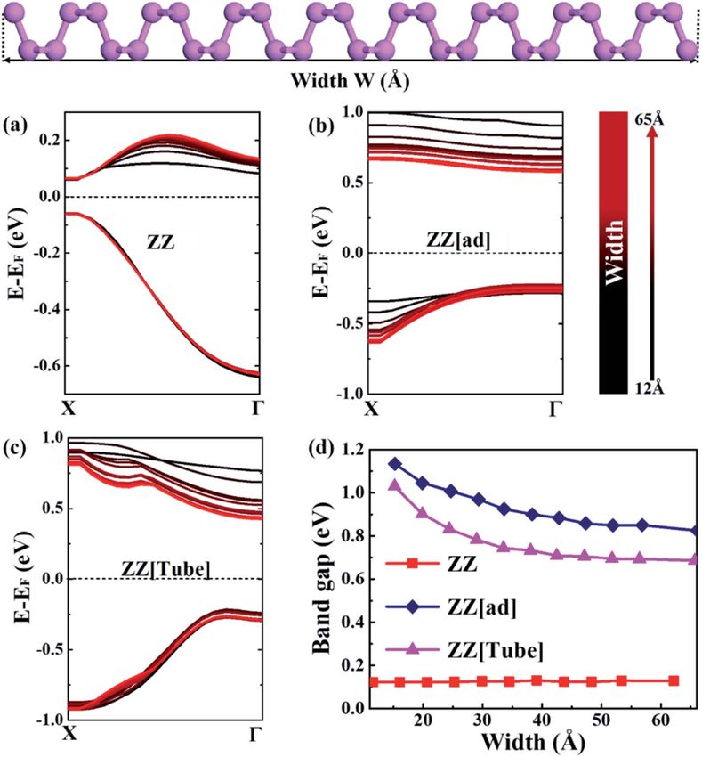
View Article Online
Paper Nanoscale Advances
a ribbon width of 15 Å (Fig. 1g–i). For ZZ PNR, the VBM does As discussed above, the ribbon width, whose denition is
not change much and the CBM shis downwards except for schematically shown in Fig. 2, has a signicant inuence on the
the value at the X point. Therefore, the band gap of ZZ PNR electronic structure of PNRs. Therefore, the changes in VBM
changes slightly (from 0.13 eV to 0.12 eV). In contrast, the and CBM with width ranging from 15 Å to 65 Å for three kinds of
This article is licensed under a Creative Commons Attribution-NonCommercial 3.0 Unported Licence.
band gaps of ZZ[ad] and ZZ[Tube] PNRs increase by 0.30 eV PNRs are plotted in Fig. 2a–c. For ZZ PNRs, the VBM does not
and 0.26 eV when the width changes from 40 Å to 15 Å. Due to change with the ribbon width and the CBM shis upwards with
the quantum connement effect, the width also alters the an increase in the width but keeping the X point xed. Thus, the
nature of the VBM and CBM, which can be visualized by band gap of ZZ PNRs is not sensitive to the ribbon width (red
charge density plotting, as shown beside each band line in Fig. 2d). For ZZ[ad] PNRs, the VBM at the G point
structure. changes slightly with the ribbon width, but the CBM drops a lot
Our band structure calculations in this paper are based on with an increase in the width, resulting in a decreasing gap with
Open Access Article. Published on 31 May 2021. Downloaded on 10/7/2021 10:47:50 PM.
the standard PBE exchange–correlation functional, which may increasing width (blue line in Fig. 2d).
underestimate the band gap. Hybrid functionals or GW calcu- In contrast, for ZZ[Tube] PNRs, the CBM drops a lot with an
lations can give more accurate band gaps.35,52,53 For example, the increase in width. As a consequence, the band gap of ZZ[Tube]
band gap of 43 Å ZZ[Tube] PNR is 0.63 eV based on PBE, while it PNRs decreases from 1.03 to 0.69 eV with an increase in width
is 1.23 eV using HSE06.36 However, the band alignment and (pink line in Fig. 2d). As shown in Fig. 2d, when the width is
dispersion curvature are quite similar for both PBE and HSE06. greater than 40 Å, the band gap does not change much any more
In addition, both PBE and HSE06 exhibit the same charge with width for all three kinds of PNRs, implying the weakness of
separation of VBM and CBM for PNR with a tube edge.36 A the quantum connement effect in very wide nanoribbons. The
previous study also found that the standard PBE can give the full band structures of ZZ, ZZ[ad] and ZZ[Tube] PNRs with
correct trend of the band gap changing from monolayer to bulk, different widths can be seen in Fig. S1, S2 and S3,† respectively.
compared with GW results.36,54,55 This paper aims to reveal the Strain engineering is also a simple and effective method of
width and strain inuence on PNRs with different edges. tuning the properties of nanoribbons. We studied the yield
Standard PBE can give a suitable band gap changing trend and stress for the three PNRs to check the strain limit before their
reveal the charge separation of VBM and CBM. The computa- impact on electronic properties. As discussed above, we chose
tional cost is huge even using standard PBE, therefore, we 40 Å wide PNRs to weaken the width effect and focused on the
cannot afford the much more costly HSE06 and GW methods strain effect, as shown in Fig. 3a (strain–stress curves for PNRs
for this in-time work. However, the more accurate electronic with different widths are shown in Fig. S4 in the ESI†). For ZZ
properties of ZZ[Tube] PNR based on HSE06 and GW are highly PNR, under a critical strain of 17%, the stress drops abruptly
deserving of future study. giving a yield stress of 14.32 GPa. The yield is due to the
Fig. 3 The stress–strain curves for ZZ, ZZ[ad] and ZZ[Tube] PNRs (a). Geometrical structures of ZZ, ZZ[ad] and ZZ[Tube] PNRs under critical strain
(b–e). Bonds highlighted in yellow are those that undergo a rotation under critical strain.
© 2021 The Author(s). Published by the Royal Society of Chemistry Nanoscale Adv., 2021, 3, 4416–4423 | 4419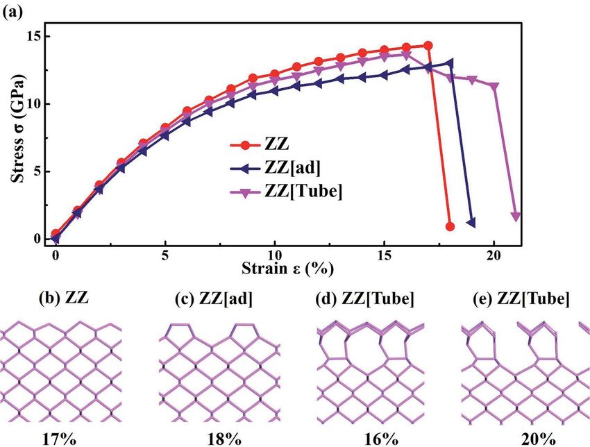
View Article Online
Nanoscale Advances Paper
structural change with bond rotation, as shown in Fig. 3b. A fracture behavior. To verify its stability, we performed AIMD
similar structural change occurs in ZZ[ad] PNR under a critical for ZZ[Tube] PNRs under 4% strain (Fig. S6†). The tempera-
strain of 18% (Fig. 3c) resulting in a yield stress of 13.03 GPa ture is around 300 K. Aer 9 ps simulations, the ZZ[Tube]
(Fig. 3a). PNRs are completely retained. We then further simulated PNR
This article is licensed under a Creative Commons Attribution-NonCommercial 3.0 Unported Licence.
In sharp contrast, there are two critical points for ZZ[Tube] with ZZ[Tube] under 15% (Fig. S6b†), 16% (Fig. S6c†) and 17%
PNR, i.e. 16% and 20%. When the strain reaches 16%, partial (Fig. S6d†) strains at T ¼ 300 K through AIMD. Aer 5 ps
chemical bonds at the edges break, leading to a slight drop in simulations, the structure is still very stable under 15%
stress. Then the stress slowly decreases with increasing strain, (Fig. S6b†) and 16% (Fig. S6c†) strain. Under 17% strain, the
keeping the geometry of the middle part of the ribbon the same tube edges are broken, while the inner phosphorene is still
as that in bulk phosphorene. When the strain reaches 20%, stable. These results are the same as those for structural
a similar structural change occurs to that in ZZ PNRs, resulting relaxation, meaning that PNR under 17% strain is not broken.
Open Access Article. Published on 31 May 2021. Downloaded on 10/7/2021 10:47:50 PM.
in a sharp drop in the stress and a yield stress of 11.33 GPa. This is similar to previous studies, which indicate that PNR
Therefore, compared with ZZ and ZZ[ad] PNRs, ZZ[Tube] PNR can afford a large strain in the ZZ direction.56 However, plastic
has a smaller yield stress and stronger exibility. The detailed structural transformation will occur when the strain is over
structural deformation of ZZ, ZZ[Tube] and ZZ[ad] PNRs during 21%.
stretching can be found in Fig. S5 in the ESI.† All three edge Next, we explore the strain effect on the electronic structure
reconstructed PNRs have stronger exibility compared with of PNRs before fracture. Fig. 4a–c show VBM and CBM of PNRs
unconstructed PNRs.47 with different edges under variable strain/compression. For ZZ
The above mechanical properties are the ideal mechanical PNR, under a compressive strain from 1% to 4%, the PNR is
properties of PNRs using an adiabatic approximation. The an indirect semiconductor. When the compressive strain rea-
results are only correct at very low temperature. Under ches 5%, the PNR becomes metallic with the conduction band
common conditions, temperature may seriously affect the crossing the Fermi level. Under a tensile strain (0% to 9%), the
Fig. 4 The changes in VBM and CBM with strain for ZZ, ZZ[ad] and ZZ[Tube] PNRs with a width of 40 Å (a–c). The horizontal dashed lines indicate
the Fermi level. The band gaps of ZZ, ZZ[ad] and ZZ[Tube] PNRs are a function of strain (d). The solid blue line is the linear fitting of the relation
between the band gap Eg and the strain 3.
4420 | Nanoscale Adv., 2021, 3, 4416–4423 © 2021 The Author(s). Published by the Royal Society of Chemistry
View Article Online
Paper Nanoscale Advances
PNR is a direct semiconductor with the CBM and VBM at the X strain is over 5%, the directions of shi of the CBM and VBM are
point. Both VBM and CBM drop with an increase in strain, reversed and thus the band gap starts to decrease.
resulting in a nearly unchanged band gap with increasing As shown in Fig. 1f and i, the VBM and CBM charges are
tensile stress (Fig. 4d). spatially separated for the ZZ[Tube] PNRs with variable widths.
This article is licensed under a Creative Commons Attribution-NonCommercial 3.0 Unported Licence.
For ZZ[ad] PNR, the CBM is not sensitive to strain except for Another question is whether the spatial charge separation is
a very large strain of over 7% (Fig. 4b). The VBM at the G point robust under strain, which is signicant for applications. Plots
does not change much with strain even though it becomes more of the charge under strains of 5%, 0% and 4% are shown in
and more dispersive with increasing tensile stress. Therefore, Fig. 5a–c. We can conclude that the charge separation of VBM
the direct band gap of ZZ[ad] PNR does not change with a strain and CBM is quite robust and can be well preserved within
below 7%. When the strain is larger than 7%, a sudden drop in a strain range of 5% to 5% (Fig. S7†). In this strain range, the
the CBM at the G point results in a drop in the band gap, as band gap of ZZ[Tube] PNR varies from 0.13 eV to 1.18 eV. The
Open Access Article. Published on 31 May 2021. Downloaded on 10/7/2021 10:47:50 PM.
shown in Fig. 4d. optical absorption spectra of ZZ[Tube] PNR under 5%, 0% and
In sharp contrast with ZZ and ZZ[ad] PNRs, both CBM and 4% strains, are shown in Fig. 5d–f, respectively. For PNR with
VBM are very sensitive to strain for ZZ[Tube] PNR, as shown in 5%, 0% and 4% strains, the optical absorption is initially
Fig. 4c. When the strain varies from 5% to 4%, the VBM shis indirect adsorption and then the absorption coefficients
downwards and the CBM shis upwards, which results in increase sharply, implying strong direct adsorption. Such
a great increase in the band gap, from 0.13 eV to 1.18 eV strong optical absorption ranges from 9840 nm to 1050 nm,
(Fig. 4d). The relationship between the band gap Eg and the covering the near-infrared (780–3000 nm) and mid-infrared
strain 3 can be simply tted by a linear equation as Eg ¼ 0.717 + (3000–50 000 nm) zones (Fig. 5g), which is very physically
0.1233 (the solid blue line in Fig. 4d). Interestingly, when the interesting and could be technologically important. Therefore,
Fig. 5 Electronic band structures of ZZ[Tube] PNRs with a width of 40 Å under strains of 5%, 0% and 4%. The VBM and CBM are highlighted in
red and blue, respectively. The isosurface value is 1.2 104 jej bohr3 (a–c). The VBM and CBM are highlighted in red and blue, respectively. (d)–
(f) Optical absorption coefficients of ZZ[Tube] PNRs under strain at 5%, 0% and 4%. (g) A schematic diagram of a possible optoelectronics
application of ZZ[Tube] PNRs.
© 2021 The Author(s). Published by the Royal Society of Chemistry Nanoscale Adv., 2021, 3, 4416–4423 | 4421View Article Online
Nanoscale Advances Paper
an infrared photoelectric eld effect transistor (FET) working Acknowledgements
within different spectrum ranges can be constructed using ZZ
[Tube] PNRs with different widths as the conductive channel, as This work was supported by the National Natural Science
shown in Fig. 5g. The constructed FET can also be used as Foundation of China (Grant No. 12074053, 91961204,
This article is licensed under a Creative Commons Attribution-NonCommercial 3.0 Unported Licence.
a strain sensor due to the strong dependence of the band gap on 12004064), by XingLiaoYingCai Project of Liaoning province,
strain. China (XLYC1907163) and by the start-up funding (DUT20RC(3)
The lowest-energy and low formation barrier of tube-recon- 026). First-principle calculations were performed on Tianjin
struction,36 the robust spatial charge separation of VBM and Supercomputing Platform and Shanghai Supercomputing Plat-
CBM, the tunable band gap with width, linear band gap form and the Supercomputing Center of Dalian University of
response to strain, as well as the small carrier effective mass Technology.
suggest potential applications of ZZ[Tube] PNRs in optoelec-
Open Access Article. Published on 31 May 2021. Downloaded on 10/7/2021 10:47:50 PM.
tronic devices based on infrared light.57–59 When the strain References
reaches 6% (Fig. S7†), both the CBM and VBM originate from
bulk states and the charge separation disappears, which should 1 J. Qiao, X. Kong, Z. X. Hu, F. Yang and W. Ji, Nat. Commun.,
be avoided in applications. 2014, 5, 4475.
2 S. Lee, F. Yang, J. Suh, S. Yang, Y. Lee, G. Li, H. Sung Choe,
A. Suslu, Y. Chen, C. Ko, J. Park, K. Liu, J. Li,
Conclusion K. Hippalgaonkar, J. J. Urban, S. Tongay and J. Wu, Nat.
In summary, using DFT calculations, we systemically investi- Commun., 2015, 6, 8573.
gated the width and strain effects on the electronic properties of 3 L. Li, Y. Yu, G. J. Ye, Q. Ge, X. Ou, H. Wu, D. Feng, X. H. Chen
ZZ, ZZ[ad] and ZZ[Tube] PNRs. Due to the quantum conne- and Y. Zhang, Nat. Nanotechnol., 2014, 9, 372–377.
ment effect, the band gaps of ZZ[ad] and ZZ[Tube] PNRs 4 W. Li, Y. Yang, G. Zhang and Y. W. Zhang, Nano Lett., 2015,
increase with a decrease in the ribbon width. However, the 15, 1691–1697.
ribbon width has little inuence on the electronic properties of 5 F. Xia, H. Wang and Y. Jia, Nat. Commun., 2014, 5, 4458.
ZZ PNRs. Besides the ribbon width, the band gaps of ZZ[Tube] 6 S. Das, W. Zhang, M. Demarteau, A. Hoffmann, M. Dubey
PNRs can be effectively tuned by strain in sharp contrast with ZZ and A. Roelofs, Nano Lett., 2014, 14, 5733–5739.
and ZZ[ad] PNRs which are not sensitive to strain. ZZ[Tube] 7 L. Li, J. Kim, C. Jin, G. J. Ye, D. Y. Qiu, F. H. da Jornada, Z. Shi,
PNRs possess much smaller carrier effective masses (0.42 m0 for L. Chen, Z. Zhang, F. Yang, K. Watanabe, T. Taniguchi,
electrons and 1.24 m0 for holes) than ZZ[ad] PNRs and are thus W. Ren, S. G. Louie, X. H. Chen, Y. Zhang and F. Wang,
more desirable for applications. Interestingly, ZZ[Tube] PNRs Nat. Nanotechnol., 2017, 12, 21–25.
exhibit robust charge separation of VBM and CBM within 8 S. Lei, H. Wang, L. Huang, Y.-Y. Sun and S. Zhang, Nano Lett.,
a range of strain, from 5% to 5%. Therefore, ZZ[Tube] PNRs 2016, 16, 1317–1322.
have the lowest energy, and ease of formation in terms of 9 S. Susarla, A. Kutana, J. A. Hachtel, V. Kochat, A. Apte,
kinetics;36 they have a robust spatial charge separation of VBM R. Vajtai, J. C. Idrobo, B. I. Yakobson, C. S. Tiwary and
and CBM; their band gap can be tuned with width; they have P. M. Ajayan, Adv. Mater., 2017, 29, 1702457.
a linear band gap response to strain, as well as a small carrier 10 S. V. Morozov, K. S. Novoselov, M. I. Katsnelson, F. Schedin,
effective mass. Therefore, ZZ[Tube] PNRs are a comprehensively D. C. Elias, J. A. Jaszczak and A. K. Geim, Phys. Rev. Lett.,
promising candidate for microelectronic and optoelectric 2008, 100, 016602.
devices. 11 S. Wang, P. K. Ang, Z. Wang, A. L. Tang, J. T. Thong and
K. P. Loh, Nano Lett., 2010, 10, 92–98.
12 C. Yan, C. Gong, P. Wangyang, J. Chu, K. Hu, C. Li, X. Wang,
Data availability X. Du, T. Zhai, Y. Li and J. Xiong, Adv. Funct. Mater., 2018, 28,
1803305.
The authors indicate that the generated and analyzed data that
13 Y. Cai, Q. Ke, G. Zhang, Y. P. Feng, V. B. Shenoy and
support the ndings of this study are available within the paper
Y.-W. Zhang, Adv. Funct. Mater., 2015, 25, 2230–2236.
and ESI.†
14 S. Yoon, T. Kim, S.-Y. Seo, S.-H. Shin, S.-B. Song, B. J. Kim,
K. Watanabe, T. Taniguchi, G.-H. Lee, M.-H. Jo, D. Y. Qiu
Author contributions and J. Kim, Phys. Rev. B: Condens. Matter Mater. Phys.,
2021, 103, L041407.
J. Gao, Y. Su proposed this project. M. Xia carried out all the DFT 15 J. Guan, Z. Zhu and D. Tomanek, Phys. Rev. Lett., 2014, 113,
calculations. S. Li, H. Liu, L. Wang, J. Gao and J. Zhao conducted 046804.
result analysis. All authors wrote and revised this manuscript. 16 R. Fei and L. Yang, Nano Lett., 2014, 14, 2884–2889.
17 X. Wang, A. M. Jones, K. L. Seyler, V. Tran, Y. Jia, H. Zhao,
Conflicts of interest H. Wang, L. Yang, X. Xu and F. Xia, Nat. Nanotechnol.,
2015, 10, 517–521.
The authors declare no competing nancial or non-nancial 18 S. Deng, A. V. Sumant and V. Berry, Nano Today, 2018, 22, 14–
interests. 35.
4422 | Nanoscale Adv., 2021, 3, 4416–4423 © 2021 The Author(s). Published by the Royal Society of ChemistryView Article Online
Paper Nanoscale Advances
19 L. Zhu, G. Zhang and B. Li, Phys. Rev. B: Condens. Matter 39 A. Maity, A. Singh, P. Sen, A. Kibey, A. Kshirsagar and
Mater. Phys., 2014, 90, 214302. D. G. Kanhere, Phys. Rev. B, 2016, 94, 075422.
20 K. Chen, J. Deng, X. Ding, J. Sun, S. Yang and J. Z. Liu, J. Am. 40 Q. Wu, L. Shen, M. Yang, Y. Cai, Z. Huang and Y. P. Feng,
Chem. Soc., 2018, 140, 16206–16212. Phys. Rev. B: Condens. Matter Mater. Phys., 2015, 92, 035436.
This article is licensed under a Creative Commons Attribution-NonCommercial 3.0 Unported Licence.
21 F. Cheng, H. Xu, W. Xu, P. Zhou, J. Martin and K. P. Loh, 41 X. Han, H. M. Stewart, S. A. Shevlin, C. R. Catlow and
Nano Lett., 2017, 17, 1116–1120. Z. X. Guo, Nano Lett., 2014, 14, 4607–4614.
22 L. Liu, Z. Ge, C. Yan, A. D. Moghadam, M. Weinert and L. Li, 42 T. Hu, H. Wu, H. Zeng, K. Deng and E. Kan, Nano Lett., 2016,
Phys. Rev. B: Condens. Matter Mater. Phys., 2018, 98, 235304. 16, 8015–8020.
23 S. Wang, L. Talirz, C. A. Pignedoli, X. Feng, K. Mullen, 43 B. Huang, M. Liu, N. Su, J. Wu, W. Duan, B. L. Gu and F. Liu,
R. Fasel and P. Ruffieux, Nat. Commun., 2016, 7, 11507. Phys. Rev. Lett., 2009, 102, 166404.
24 B. Ostahie and A. Aldea, Phys. Rev. B: Condens. Matter Mater. 44 Z. Z. Y. Li, S. Zhang and Z. Chen, J. Am. Chem. Soc., 2008, 130,
Open Access Article. Published on 31 May 2021. Downloaded on 10/7/2021 10:47:50 PM.
Phys., 2016, 93, 075408. 16739–16744.
25 Y. Ren, X. Zhou and G. Zhou, Phys. Rev. B: Condens. Matter 45 C.-H. Park and S. G. Louie, Nano Lett., 2008, 8, 2200–2203.
Mater. Phys., 2021, 103, 045405. 46 Y. W. Son, M. L. Cohen and S. G. Louie, Phys. Rev. Lett., 2006,
26 W. Hu, L. Lin, C. Yang, J. Dai and J. Yang, Nano Lett., 2016, 97, 216803.
16, 1675–1682. 47 V. Sorkin and Y. W. Zhang, Nanotechnology, 2015, 26,
27 X. Zhang, J. Xin and F. Ding, Nanoscale, 2013, 5, 2556–2569. 235707.
28 Q. Deng and J. Zhao, Nano Lett., 2016, 16, 1244–1249. 48 H. Pan and Y.-W. Zhang, J. Phys. Chem. C, 2012, 116, 11752–
29 K. Kim, S. Coh, C. Kisielowski, M. F. Crommie, S. G. Louie, 11757.
M. L. Cohen and A. Zettl, Nat. Commun., 2013, 4, 2723. 49 J. Qi, X. Qian, L. Qi, J. Feng, D. Shi and J. Li, Nano Lett., 2012,
30 Z. Liu, Y. C. Lin, C. C. Lu, C. H. Yeh, P. W. Chiu, S. Iijima and 12, 1224–1228.
K. Suenaga, Nat. Commun., 2014, 5, 4055. 50 P. E. Blochl, Phys. Rev. B: Condens. Matter Mater. Phys., 1994,
31 P. Koskinen, S. Malola and H. Hakkinen, Phys. Rev. Lett., 50, 17953–17979.
2008, 101, 115502. 51 G. K. a. J. Furthmüller, Phys. Rev. B: Condens. Matter Mater.
32 P. Cui, J. H. Choi, W. Chen, J. Zeng, C. K. Shih, Z. Li and Phys., 1996, 54, 11169.
Z. Zhang, Nano Lett., 2017, 17, 1097–1101. 52 A. Cupo and V. Meunier, J. Phys.: Condens. Matter, 2017, 29,
33 W. Li, G. Zhang and Y.-W. Zhang, J. Phys. Chem. C, 2014, 118, 283001.
22368–22372. 53 S. I. Allec and B. M. Wong, J. Phys. Chem. Lett., 2016, 7, 4340–
34 H. Guo, N. Lu, J. Dai, X. Wu and X. C. Zeng, J. Phys. Chem. C, 4345.
2014, 118, 14051–14059. 54 Y. Cai, G. Zhang and Y. W. Zhang, Sci. Rep., 2014, 4, 6677.
35 L. Liang, J. Wang, W. Lin, B. G. Sumpter, V. Meunier and 55 V. Tran, R. Soklaski, Y. Liang and L. Yang, Phys. Rev. B:
M. Pan, Nano Lett., 2014, 14, 6400–6406. Condens. Matter Mater. Phys., 2014, 89, 235319.
36 J. Gao, X. Liu, G. Zhang and Y. W. Zhang, Nanoscale, 2016, 8, 56 M. Wu and X. C. Zeng, Nano Lett., 2016, 16, 3236–3241.
17940–17946. 57 X. Ling, H. Wang, S. Huang, F. Xia and M. S. Dresselhaus,
37 V. V. Ivanovskaya, A. Zobelli, P. Wagner, M. I. Heggie, Proc. Natl. Acad. Sci. U. S. A., 2015, 112, 4523–4530.
P. R. Briddon, M. J. Rayson and C. P. Ewels, Phys. Rev. 58 N. Youngblood, C. Chen, S. J. Koester and M. Li, Nat.
Lett., 2011, 107, 065502. Photonics, 2015, 9, 247–252.
38 X. Liu, J. Gao, G. Zhang and Y.-W. Zhang, Adv. Funct. Mater., 59 A. S. Rodin, A. Carvalho and A. H. Castro Neto, Phys. Rev.
2017, 27, 1702776. Lett., 2014, 112, 176801.
© 2021 The Author(s). Published by the Royal Society of Chemistry Nanoscale Adv., 2021, 3, 4416–4423 | 4423You can also read