Phase signature of topological transition in Josephson Junctions
←
→
Page content transcription
If your browser does not render page correctly, please read the page content below
Phase signature of topological transition in Josephson Junctions

                                                                               William Mayer1∗ , Matthieu C. Dartiailh1∗ , Joseph Yuan1 ,
                                                                  Kaushini S. Wickramasinghe1 , Alex Matos-Abiague2 , Igor Žutić3 , and Javad Shabani1
                                                                  1
                                                                   Center for Quantum Phenomena, Department of Physics, New York University, NY 10003, USA
                                                                      2
                                                                        Department of Physics & Astronomy, Wayne State University, Detroit, MI 48201, USA
arXiv:1906.01179v1 [cond-mat.mes-hall] 4 Jun 2019

                                                           3
                                                               Department of Physics, University at Buffalo, State University of New York, Buffalo, New York 14260, USA
                                                                                        ∗
                                                                                           These authors contributed equally to this work
                                                                                                        (Dated: June 5, 2019)

                                                       Topological superconductivity hosts exotic quasi-particle excitations including Majorana bound states
                                                    which hold promise for fault-tolerant quantum computing. The theory predicts emergence of Majorana
                                                    bound states is accompanied by a topological phase transition. We show experimentally in epitaxial Al/InAs
                                                    Josephson junctions a transition between trivial and topological superconductivity. We observe a minimum
                                                    of the critical current at the topological transition, indicating a closing and reopening of the supercond-
                                                    cuting gap induced in InAs, with increasing magnetic field. By embedding the Josephson junction in a
                                                    phase-sensitive loop geometry, we measure a π-jump in the superconducting phase across the junction when
                                                    the system is driven through the topological transition. These findings reveal a versatile two-dimensional
                                                    platform for scalable topological quantum computing.
                                                       Majorana bound states (MBS), which are their own antiparticles, are predicted to emerge as zero-energy modes
                                                    localized at the boundary between a topological superconductor and a topologically-trivial region [1]. MBS can
                                                    nonlocally store quantum information and their non-Abelian exchange statistics allows for the implementation of
                                                    quantum gates through braiding operations [2]. This makes them ideal candidates for robust qubits in fault-tolerant
                                                    topological quantum computing [3]. Rather than seeking elusive spinless p-wave superconductors required for
                                                    MBS, a common approach is to use conventional s-wave superconductors to proximity-modify semiconductor
                                                    heterostructures with the suitable symmetries [4].
                                                       Early proposals to realize MBS were focused on one-dimensional (1D) systems such as proximitized nanowires
                                                    and atomic chains [5–9], where the observation of a quantized zero-bias conductance peak [10] provided the sup-
                                                    port for MBS. However, the inherent difficulties in the technological implementation of the required networks,
                                                    together with the intrinsic instabilities of their 1D elements, have motivated the search for versatile 2D platforms
                                                    exploiting the use of more conventional devices such as Josephson junctions (JJs) and spin valves [11–14]. Re-
                                                    cent experiments [15–17] suggest that planar JJs are particularly promising because they support the transition to
                                                    topological superconductivity over a large range of external parameters without requiring fine tuning.
                                                       In this work, we observe a minimum of the critical current in a JJ with increasing parallel (in-plane) magnetic
                                                    field, Bk , which indicates a closing and reopening of the superconducting gap. This minimum is accompanied by
                                                    a π-jump in the superconducting phase across the junction. This only occurs when Bk is applied perpendicular
                                                    to the current direction. Both signatures, in a material with spin-orbit coupling (SOC), suggest that the gap that
                                                    opens at high Bk is topological in nature. Theoretical simulations provide additional support for the presence of
                                                    a topological transition and its compatibility with the emergence of MBS. Details of the model used are presented
                                                    in Supplementary Materials. The topological phase appears resilient to small field misalignments, demonstrating
                                                    potential for more complicated geometries and MBS braiding. In addition to Bk amplitude, the top gate voltage is
                                                    demonstrated to be an efficient control knob for manipulating the topological phase transition.
                                                       We investigate planar JJs based on epitaxial Al/InAs, engineered to support high-interfacial transparency and
                                                    robust proximity-induced superconductivity in InAs [11]. To explore potential phase-sensitive signatures of topo-
                                                    logical superconductivity, we use two JJs to form a superconducting quantum interference device (SQUID) as
                                                    shown by a SEM image in Fig. 1A. We should note that the SQUID phase-measurements were crucial for identi-
                                                    fying unconventional superconductivity in cuprates [18]. Both junctions (1, 2) of the SQUID are W=4 µm wide
                                                    and L=100 nm long, while the area of the SQUID loop is 25 µm2 . The two junctions show small variations in
                                                    normal resistance(Rn ), Rn1 = 102 Ω, Rn2 = 110 Ω and critical current(Ic ) Ic1 = 4.4 µA, Ic2 = 3.6 µA, measured in
                                                    the absence of a gate voltage. Using a vector magnet, we can apply an in-plane field along an arbitrary axis defined
                                                    by θ as indicated in Fig. 1A and phase-bias our device. The versatility of our setup can be seen from the measured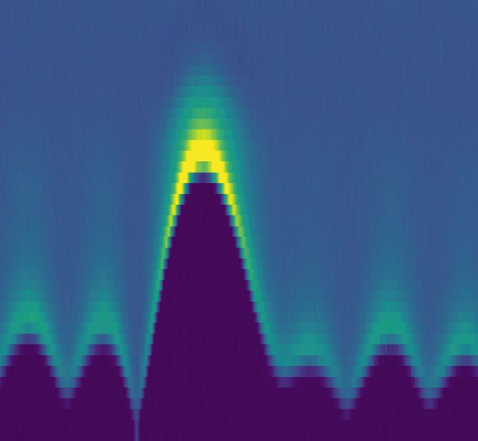
2

A                                           B                                        Resistance (Ω)                          C
            Vg1                                                                                                       JJ 1
                                                                            0       20   40   60       80   100
                                                                    0                                             I
                   W = 4 µm
                                                                                                                                          1.2

                                             Gate voltage Vg2 (V)
                                                                                                                      JJ 2
                                                               -2

                                                                                                                                 By (T)
    I                                                                                                                                     0.8
                  y θ
                                                               -4
                              x                                                                                                           0.4
                                                                                                                      JJ 1
              L = 100 nm                                       -6
                                                                                                                  I
                                                                                                                                          0.0
                                                                        0       2        4         6        8                                   -1.0   -0.5      0.0       0.5   1.0
                              V   g
                                   2
                                                                                    Bias current (µA)                                                         Ic / Ic(0)

Fig. 1: Physical system (A) SEM image (colorized) of a SQUID similar to the one presented. The device is composed of
two 4 µm wide JJ with a gap of 100 nm. The central area is about 25 µm2 and each junction is independently gateable. The
x direction is taken colinear to the current flow in the junctions. (B) Measurement of the junction resistance at zero flux as a
function of the gate voltage applied on JJ2. At Vg2 = 0 V both junctions can carry a supercurrent, below Vg2 < −5.5 V, JJ2
behaves like an open circuit. (C) Predicted critical current of a junction in the presence of an in-plane field along y. Above the
first dashed line, the superconducting state goes from s to p-type and goes back to s-type above the second dashed line.

SQUID resistance as a function of an applied bias current, I, and Vg2 in Fig. 1B. The critical current, at which the
SQUID acquires a finite resistance, decreases and becomes constant for Vg2 < −5.5 V, indicating that JJ2 is fully
depleted. This shows that each JJ can be studied individually. Additional data demonstrating that we can operate
this device either as a SQUID or as a single JJ are presented in Supplementary Materials.
   In the presence of Bk ≡ By , theory predicts a single junction will undergo a topological phase transition. One
signature of this transition is the closing (or partial closing) and re-opening of the superconducting gap as illustrated
in the tight-binding simulation results presented in Fig. 1C. Above that closing, we expect the superconducting state
to have transitioned towards a topological phase dominated by chiral p-type superconductivity.
   Our characterization of JJs in Bk shows that both have the same critical magnetic field Bc ≈ 1.45 T, for thin-film
Al, and independent of the Bk direction. In contrast, both junctions show strong anisotropy of Ic with Bk direction
as shown in Supplementary Materials. These findings are consistent with the previous measurements on JJs based
on InAs 2DEG [12]. In Fig. 2A and B, we present the dependence of the critical current of JJ1 as a function of
By at two different gate voltages: (A) Vg1 = −1.5 V and (B) Vg1 = 1.4 V. In Fig. 2A, at lower Vg1 and thus at a
lower density, we observe a trivial monotonic decrease of Ic with By . Remarkably, at higher Vg1 in Fig. 2B we see
a striking difference where the superconducting gap closes and reopens around By = 600 mT, in agreement with
the tight-binding results from Fig. 1C. Above that gap closing, we measure Ic ∼ 20 nA, consistent with the gap
reopening and topological transition. A similar non-monotonic gap dependence with Bk was recently reported in
HgTe [19] and InSb [17].
   By considering Thouless energy, ET = (π/2)vF /L, where vF is the Fermi velocity and L is the gap of the
junction, one may expect to reach the topological phase more easily at low density (smaller gate voltages) since
the transition has been predicted to occur around EZ ∼ ET , where EZ is the Zeeman energy [20]. However,
this neglects the vF -mismatch between the Al and InAs regions [21], and SOC [22], which can both change with
density [23].
   The nontrivial evolution of the superconducting gap and topological transition show similar behaviour in both
junctions (JJ1 and JJ2). Figure 2C presents the zero-bias resistance of JJ2 as a function Vg2 and By . At the largest
Vg2 , the transition occurs at ∼ 500 mT and moves towards higher By , as Vg2 is decreased. Below Vg2 = −1.5 V no
evidence of any transition remains. The lower magnetic field transition in JJ2 compared to JJ1 can be attributed to
small variation of junction properties for example lower supercurrent and corresponding induced gap.
   While the observed non-monotonic dependence of Ic with By is consistent with a transition to topological
superconductivity, phase-sensitive measurements with a SQUID could independently confirm this scenario. How-
ever, it is generally difficult to avoid arbitrary field offsets between measurements. Here, following the approach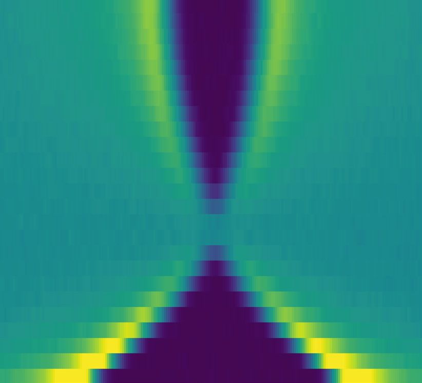
3
A Gate voltage Vg1 = -1.5 V
B Gate voltage Vg1 = 1.4 V
1.2
JJ 1 100
JJ 1
In-plane field By (T)
1.0 I I 80
Resistance (Ω)
0.8
60
0.6
40
0.4
20
0.2
0
-4 -2 0 2 4 -4 -2 0 2 4
Bias current (µA) Bias current (µA)
C 4
70
Zero-bias resistance (Ω)
s-type p-type
Gate voltage Vg2 (V)
2
50
0
30
I
-2 10
JJ 2
0.0 0.2 0.4 0.6 0.8 1.0 1.2 1.4
In-plane field By (T)
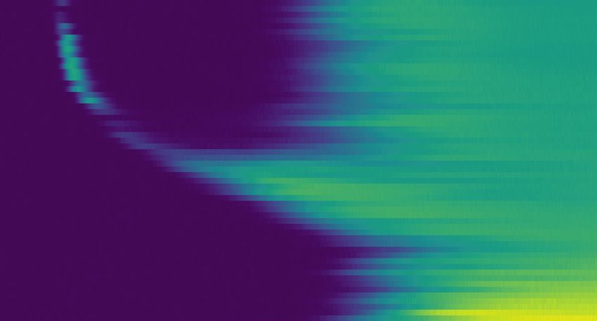
Fig. 2: Re-opening of superconducting gap in magnetic field Measurement of the resistance of JJ1 as function of an applied
in-plane field along the y-axis at two different gate voltages (A) Vg1 = −1.5 V, (B) Vg1 = 1.4 V. In both cases, JJ2 is depleted
(Vg2 = −7 V) and does not participate in the transport. At high gate (B), a closing and re-opening of the superconducting gap is
observed around 600 mT for JJ1. (C) Zero-bias resistance of JJ2 as a function of the applied in-plane field and the gate voltage.
At low gate, the superconducting gap remains open up to about 1T. At higher gates a gap closing and re-opening characterized
by a peak in resistance appears and moves to lower fields as the gate increases. Vg1 is set to -7V.
described in [24], we use the gate tunability of our device to measure the phase offset between the oscillations
observed at different gate voltage but acquired during a single Bz sweep. Using SQUID interferometry, we can
identify topological transition by setting JJ1 at Vg1 = −2 V as the reference junction. At this gate voltage, JJ1
does not show a topological transition at any field By . The resulting SQUID oscillations in JJ2 reveal some crucial
differences between By = 100 mT and 850 mT, shown respectively in Figs. 3A and 3B, for various Vg2 . From the
results in Fig. 2C, we expect that JJ2 would never reach the topological regime at 100 mT. Indeed, in Fig. 3A, we
only observe a small phase-shift which we attribute to the spin-galvanic effect, discussed in [24]. At higher By
in Fig. 3B there is a larger phase-shift between Vg2 = −3 V and -4 V than in Fig. 3A, consistent with the linear
increase of spin-galvanic effect in By . However, comparing Vg2 = −1 V and higher gate values, one can note that
a phase-shift of about π occurs. This independently supports the transition to the topological phase shown for the
same parameter range in Fig. 2C.
Our tight-binding calculations, presented in Fig. 3C, reveal that such a nearly π-jump in the superconducting
phase is indeed a fingerprint expected for the topological transition with the emergence of MBS, shown in Supple-
mentary Materials. Consistent with previous findings [15, 20], our simulation predicts a phase-dependent position
of the gap closing in a phase-biased system, as indicted by the purple line in Fig. 3C. In Fig. 3D we present the
phase-shift between the reference scan performed at Vg2 = −4 V and subsequent gate values. At low By , below
the topological transition, we observe that the phase is linear in By , as indicated by the solid lines corresponding
to linear fits to the values below 450 mT. The increase in slope with Vg2 can be attributed to the increase of SOC
[24]. For Vg2 = −3 V and −1 V, the linear trend holds up over all By . However, for Vg2 = 1 V, 2 V and 3 V, a jump
can be observed around 550 mT, followed by another linear portion. To separate these effects, we first unwrap the
phase and then subtract the linear component extracted from low-By fits. The re-plotted results in Fig. 3E reveal
near π phase-jump around the observed topological transition, consistent with theoretical predictions.
A distinct feature of the observed topological transition is its interplay of SOC and Bk . In our material the
topological regime is expected when Bk is along the y-direction, i.e. θ = 0. We test this by probing the gap
4
A B C
Resistance (Ω) Resistance (Ω)
2.0π φGS
By = 100 mT 0 20
By = 850 mT 0 20 40 φS (τ = 0)
1.5π φS (τ = 0.9)
Vg2 = 2.0 V
5.0 1.0π
φ
0.1 0.5π
2.5
0.0
0.0 0.0
0.0 0.4 0.8 1.2
Vg = 0.0 V
2
In-plane field By (T)
5.0 D
Phase-shift (reference Vg2 = -4 V)
0.1 π
2.5 Vg2 =
-3.0 V 2.0 V
Bias current (µA)
0.0 0.0 0.5π
-1.0 V 3.0 V
Vg2 = -1.0 V 1.0 V
0
5.0
0.1 -0.5π
2.5
0.0 0.0 -π
Vg2 = -3.0 V 0 200 400 600 800
5.0 In-plane field By (mT)
0.1 E
2π
2.5 Vg2 =
Corrected phase-shift
1.5π -3.0 V 2.0 V
0.0 0.0 -1.0 V 3.0 V
Vg2 = -4.0 V 1.0 V
5.0 π
0.1
2.5 0.5π
0.0 0.0 0
-6π -5π -4π -3π -2π -π 0 -2π -π 0 π 2π 3π 4π
0 200 400 600 800
SQUID phase SQUID phase In-plane field By (mT)
Fig. 3: Phase signature of topological transition from SQUID interferometry (A-B) SQUID oscillations for By = 100 mT
(A) and 850 mT (B) for different Vg2 and Vg1 = −2 V. The dashed lines indicate the position of the maximum at Vg2 = −4 V
used as a phase reference. The stars mark the position of the maximum of the oscillation. The solid orange lines are best fits to
the SQUID oscillations used to extract the period and the phase shift between different Vg2 values. (C) Ground-state phase (red
solid line) and calculated SQUID phase-shift (blue and green dashed lines), see Supplementary Materials, as a function of the
in-plane field calculated using a tight-binding model. A phase jump of about π occurs at the field corresponding to the closing
of the gap identified in Fig. 1C. Purple lines indicate the phase and field at which the zero-temperature energy gap closes in
a phase-biased system. (D) Phase difference between the SQUID oscillation at Vg2 = −4 V and the oscillation at a different
value as a function of By . The solid lines correspond to linear fits of the data for By ≤ 450 mT. (E) Phase shift from which the
linear By -contribution has been subtracted to highlight the phase jump occurring for the two higher Vg2 values.
closing in a tilted Bk , away from By . In Fig. 4 we show zoom-ins of the gap-closing of JJ1 at Vg1 = 1.4 V at
different angles. As θ is increased, the closing of the gap is weakened. Similarly, SQUID data at θ = 10◦ , shown
in Supplementary Materials, display a reduced phase-shift, which may indicate a reduced topological gap. Unlike
at smaller angles, at θ = 20◦ the gap decreases monotonically which suggests that s-wave order prevails and no
transition is observed.
In conclusion, we have presented a study of the closing and re-opening of the superconducting gap in Josephson
junctions fabricated on Al/InAs. By embedding the junction in a SQUID loop, we are able to measure the π-jump
that accompanies the re-opening of the gap. These findings strongly supports the emergence of a topological
phase in the system. This offers a scalable platform for detection and manipulation of Majorana bounds states for
development of complex circuits for fault-tolerant topological quantum computing. The versatility of this two-
dimensional geometry and SQUID manipulation may also support other exotic phases probed by phase-sensitive
signatures [25].
This work is supported by DARPA Topological Excitations in Electronics (TEE) program. This work was
performed in part at the Advanced Science Research Center NanoFabrication Facility of the Graduate Center at
5

                                                                                   θ = 0˚                         θ = -8.7˚

                                In-plane field By (mT)
                                                         700

                                                         650

                                                         600                                                                   100

                                                         550                                                                   80

                                                                                                                                   Resistance (Ω)
                                                         500                                                                   60

                                                                                  θ = 10˚                          θ = 20˚     40
                                In-plane field By (mT)

                                                         700
                                                                                                                               20
                                                         650
                                                                                                                               0
                                                         600

                                                         550

                                                         500
                                                           -200   -100    0      100    200 -200   -100    0      100    200
                                                                   Bias current (µA)                Bias current (µA)

Fig. 4: In-plane magnetic-field anisotropy of the gap closing. Resistance of JJ1 as function of the bias current and the
y-component of Bk , applied at an angle θ with respect to the y-direction as depicted in Fig. 1A.

the City University of New York.

 [1]   A. Y. Kitaev, Phys.-Usp. 44, 131 (2001).
 [2]   C. Nayak, S. H. Simon, A. Stern, M. Freedman, S. Das Sarma, Rev. Mod. Phys. 80, 1083 (2008).
 [3]   D. Aasen, et al., Phys. Rev. X 6, 031016 (2016).
 [4]   L. Fu, C. L. Kane, Phys. Rev. Lett. 100, 096407 (2008).
 [5]   R. M. Lutchyn, J. D. Sau, S. Das Sarma, Phys. Rev. Lett. 105, 077001 (2010).
 [6]   Y. Oreg, G. Refael, F. von Oppen, Phys. Rev. Lett. 105, 177002 (2010).
 [7]   V. Mourik, et al., Science 336, 1003 (2012).
 [8]   L. P. Rokhinson, X. Liu, J. K. Furdyna, Nature Physics 8, 795 (2012).
 [9]   S. Nadj-Perge, et al., Science 346, 602 (2014).
[10]   K. Sengupta, I. Žutić, H.-J. Kwon, V. M. Yakovenko, S. Das Sarma, Phys. Rev. B 63, 144531 (2001).
[11]   J. Shabani, et al., Phys. Rev. B 93, 155402 (2016).
[12]   H. J. Suominen, et al., Phys. Rev. B 95, 035307 (2017).
[13]   G. L. Fatin, A. Matos-Abiague, B. Scharf, I. Žutić, Phys. Rev. Lett. 117, 077002 (2016).
[14]   A. Matos-Abiague, et al., Solid State Communications 262, 1 (2017).
[15]   H. Ren, et al., Nature 569, 93 (2019).
[16]   A. Fornieri, et al., Nature 569, 89 (2019).
[17]   C. T. Ke, et al., arXiv:1902.10742 [cond-mat] (2019). ArXiv: 1902.10742.
[18]   C. C. Tsuei, J. R. Kirtley, Rev. Mod. Phys. 72, 969 (2000).
[19]   S. Hart, et al., Nature Physics 13, 87 (2017).
[20]   F. Pientka, et al., Phys. Rev. X 7, 021032 (2017).
[21]   I. Žutić, S. Das Sarma, Phys. Rev. B 60, R16322 (1999).
[22]   F. Setiawan, C.-T. Wu, K. Levin, Phys. Rev. B 99, 174511 (2019).
[23]   K. S. Wickramasinghe, et al., Appl. Phys. Lett. 113, 262104 (2018).
[24]   W. Mayer, et al., arXiv:1905.12670 [cond-mat] (2019). ArXiv: 1905.12670.
[25]   J. Klinovaja, D. Loss, Phys. Rev. B 90, 045118 (2014).
[26]   C. W. Groth, M. Wimmer, A. R. Akhmerov, X. Waintal, New J. Phys. 16, 063065 (2014).
[27]   J. Bardeen, R. Kümmel, A. E. Jacobs, L. Tewordt, Phys. Rev. 187, 556 (1969).
[28]   C. W. J. Beenakker, Transport Phenomena in Mesoscopic Systems (Springer, 1992), pp. 235–253.
6
Supplementary materials
I. MATERIALS AND METHODS
A. Growth and fabrication
The Josephson junction (JJ) structure is grown on semi-insulating InP (100) substrate. This is followed by a
graded buffer layer. The quantum well consists of a 4 nm layer of InAs grown on a 6 nm layer of In0.81 Ga0.25 As.
The InAs layer is capped by a 10 nm In0.81 Ga0.25 As layer which has been found to produce an optimal interface
while maintaining high 2DEG mobility [23]. This is followed by in situ growth of epitaxial Al (111). Molecular
beam epitaxy allows growth of thin films of Al where the in-plane critical field can exceed 2 T [11].
Devices are patterned by electron beam lithography using PMMA resist. Transene type D is used for wet etching
of Al and a III-V wet etch (H2 O : C6 H8 O7 : H3 P O4 : H2 O2 ) is used to define deep semiconductor mesas. We
deposit 50 nm of AlOx using atomic layer deposition to isolate gate electrodes. Top gate electrodes consisting of
5 nm Ti and 70nm Au are deposited by electron beam deposition.
Vg
Ti/Au
Al AlOx Al
In0.81Ga0.19As (10 nm)
InAs (4 nm)
In0.81Ga0.19As (6 nm)
Si
In0.81Al0.19As
Fig. S1: Structure of the fabricated Josephson Junction
B. Measurements
The device has been measured in an Oxford Triton dilution refrigerator fitted with a 6-3-1.5 T vector magnet
which has a base temperature of 7 mK. All transport measurements are performed using standard dc and lock-in
techniques at low frequencies and excitation current Iac = 10 nA. Measurements are taken in a current-biased
configuration by measuring R=dV/dI with Iac , while sweeping Idc . This allows us to find the critical current at
which the junction or SQUID switches from the superconducting to resistive state. It should be noted we directly
measure the switching current, which can be lower than the critical current due to effects of noise. For the purposes
of this study we assume they are equivalent.7
II. ADDITIONAL EXPERIMENTAL RESULTS
A. Operation of the SQUID as a single junction
The device described through the paper is a SQUID whose both junctions (JJ1, JJ2) can be gated independently.
In Fig. S2, we illustrate how we can go from a SQUID regime in which fast SQUID oscillations are clearly visible
atop the Fraunhoffer pattern of the junctions (A), to a single junction regime in which SQUID oscillations are
completely absent but we preserve the Fraunhoffer pattern of the junction which is not depleted (B).
A B
Bias current (µA)
Bias current (µA)
Resistance (Ω)
Resistance (Ω)
6 Vg = 0 V
1
Vg1 = 0 V
40 4 40
Vg2 = 0 V Vg2 = -7 V
4
20 2 20
2
0 0 0 0
−1 0 1 2 3 −1 0 1 2 3
Perpendicular field (mT) Perpendicular field (mT)
Fig. S2: SQUID to single junction transition.(A) SQUID oscillations of the device when both Josephson junctions are not
gated and in the absence of in-plane field. (B) Equivalent scan when JJ2 is fully depleted by applying -7 V on Vg2 which reduces
to Fraunhoffer pattern.
B. Fraunhofer pattern in the presence of a parallel magnetic field
The application of an in-plane magnetic field on the sample leads to a reduction of the critical current of the
Josephson junctions and a distortion of the Fraunhoffer pattern as illustrated in Fig S3.
A Parallel field Bx 250 mT B Parallel Field By 500 mT
400 400
120 120
Bias current (nA)
Bias current (nA)
Resistance (Ω)
Resistance (Ω)
300 300
80 80
200 200
100 40 100 40
0 0 0 0
-1.0 0.0 1.0 -1.0 0.0 1.0
Perpendicular field (mT) Perpendicular field (mT)
Fig. S3: Fraunhofer pattern of JJ 1 in the presence of an in-plane field. (A) Fraunhofer pattern when applying 250 mT
along the x-direction i.e. parrallel to the current. (B) Fraunhofer pattern when applying 500 mT along the y-direction.
The change in the critical current of the JJ appears to strongly depends on the direction of the applied in-plane
field. In Fig. S3, the amplitude of the critical current is similar in both plots but the magnitude of the applied
magnetic field is twice as large in the y direction (A) compared to the x direction (B).
For both directions of the field, the Fraunhoffer pattern appears asymmetric which is not the case in the absence
of the in-plane as illustrated in the main text. The observed distortions are similar for both orientation of the field.
When comparing those data to the ones presented in the main text, one can notice that the width of the first
node has been divided by about two. We attribute this effect, which is also visible in the SQUID oscillations, to
the transition out of the superconducting state of the indium layer at the back of the sample. The transition occurs
around 30 mT and does not impact our study otherwise.8
C. Gap closing at finite magnetic field driven by gate voltage
As illustrated in Fig. 2 of the main text, one can drive the system from the trivial state to the topological state at a
finite field by increasing the gate voltage resulting in both an increase of the electronic density and in an increase of
spin-orbit coupling strength. In Fig. S4, we present the superconducting gap closing and re-opening as a function
of the gate voltage applied to the junction in the presence of a parallel field of 750 mT applied along the y-axis.
In-plane field By = 0 mT In-plane field By = 750 mT
0 4 800
-1
Gate voltage Vg2 (V)
2 600
Resistance (Ω)
-2
0
-3 400
-4 -2
200
-5
-4
-6 0
-5.0 -2.5 0.0 2.5 5.0 -200 -100 0 100 200
Bias current (µA) Bias current (nA)
Fig. S4: Gate driven topological transition. Measured JJ2 resistance as a function the applied gate voltage in the absence and
presence of in-plane field of 750 mT along the y direction. The JJ 1 is depleted by applying Vg1 = −7 V.
D. Phase jump across the gap closing: Magnetic field applied at θ = 10◦
We observe in Fig. 4 that the partial closing of the superconducting gap survives up to an angle of θ ∼ 10◦ ,
away from the y-direction. We present in Fig. S5 the measured phase jump through the transition. While a phase
jump can be observed, its magnitude is reduced compared to the perfectly aligned (θ = 0◦ ) situation.
III. THEORETICAL CALCULATION DETAILS
Theoretical simulations of a single Josephson junction were performed by using the Bogoliubov-de Gennes
Hamiltonian,
g ∗ µB
2
p α
H= ∗
− µS + (p σ
y x − p σ
x y ) + V0 (x) τz − B · σ + ∆(x)τ+ + ∆∗ (x)τ− , (1)
2m ~ 2
where p is the momentum, µS the chemical potential in the S region, α is the Rashba SOC strength, B is the
external magnetic field, and m∗ = 0.03 m0 and g ∗ = 10 are the electron effective mass and effective g-factor in
InAs, respectively. The function V0 (x) = (µS − µN )Θ(L/2 − |x|) describes the changes in the N-region chemical
potential (µN ) due to the application of the gate voltage, while ∆(x) = ∆ei sgn(x)φ/2 Θ(|x| − W/2) accounts for
the spatial dependence of the superconducting gap amplitude and the corresponding phase difference (φ). The τ -
matrices are the Nambu matrices in the electron-hole space and τ± = (τx ± τy )/2. The eigenvalue problem for the
BdG Hamiltonian is numerically solved by using a finite-difference scheme on a discretized lattice as implemented
in Kwant [26], with a lattice constant a = 10 nm. The calculated eigenenergies (En ) are then used to compute the
free energy [27, 28],
X
En
F = −2kB T ln 2 cosh . (2)
2kB T
En >09
A Magnetic field applied along θ = 10 ˚
Phase-shift (reference value Vg2= -4 V)
π
Vg2 = -3.0 V
Vg2 = -1.0 V
0.5π
Vg2 = 1.0 V
Vg2 = 3.0 V
0
-0.5π
-π
0 100 200 300 400 500 600 700 800
In-plane field By (mT)
B 2π
Vg2 = -3.0 V
Vg2 = -1.0 V
Corrected phase-shift
1.5π Vg2 = 1.0 V
Vg2 = 3.0 V
π
0.5π
0
0 100 200 300 400 500 600 700
In-plane field By (mT)
Fig. S5: Phase jump in the presence of a misaligned field (A) Phase difference between the SQUID oscillation at Vg2 = −4V
and the oscillation at a different value as a function of the applied in-plane field along the y direction. The field is applied with
a 10◦ angle with respect to y-direction. The solid lines correspond to linear fits on the data for By ≤ 450 mT. (B) Phase shift
from which the contribution linear in the magnetic field has been subtracted to highlight the phase jump.
and the supercurrent,
2e dF
I(φ) = . (3)
~ dφ
The ground state phase (φGS ) is the phase that minimizes the free energy and the critical current (Ic ) corresponds
to the maximum of the supercurrent with respect to the phase, i.e. Ic = maxφ I(φ).
The temperature and magnetic field dependences of the superconducting gap are taken into account by using the
BCS relation,
s 2
B
∆(T, B) ≈ ∆(T, 0) 1 − , (4)
Bc (T )
where
" r #
Tc
∆(T, 0) ≈ ∆0 tanh 1.74 −1 . (5)
T
Here ∆0 = 1.74kB Tc with Tc as the superconductor critical temperature. The temperature dependence of the
critical magnetic field is approximated as,
" 2 #
T
Bc (T ) = Bc 1 − , (6)
Tc10
where Bc is the critical magnetic field at zero temperature.
A B
1.6 4 1.0
0.8
1.2 3
0.6
y (nm)
B (T)
0.8 2
0.4
0.4 1
0.2
0.0 0 0.0
-0.5 0.0 0.5 0 200 400 600
E/Δ x (nm)
Fig. S6: Simulations results (A) Magnetic field dependence of the low-energy ground-state spectrum of a JJ. The energy gap
closes and reopens at the field value for which φGS starts to shift from zero to nearly π (see Fig. 3C in the main text), indicating
a topological phase transition and the emergence of Majorana bound states (MBS). The red lines indicate the evolution of
finite-energy states into MBS inside the topological gap. (B) Probability density of the MBS in the JJ for B = 0.7 T (see black
dashed line in (A)). The probability density, which has been normalized to its maximum value, clearly indicated the formation
of MBS localized at the end of the junction. The green dashed lines indicate the edges of the normal region.
For the numerical simulations we used µS = µN = 0.5 meV, ∆0 = 0.23 meV, α = 10 meV nm, and
Bc = 1.6 T. For the calculation of the critical current, we used periodic boundary conditions along the junction
and assumed kB T = 0.3∆0 .
Figure S6A presents the magnetic field dependence of the low-energy ground-state spectrum, i.e. the spectrum
calculated when the phase difference across the junction equals φGS and the corresponding free energy is min-
imized. At low field φGS ≈ 0 the JJ is in the topologically trivial states with no MBS. As the field increases,
the energy gap closes and reopens at a field of about 0.5 T, indicating a topological phase transition in which
finite-energy states evolve into MBS (red lines) residing inside the topological gap. The topological transition is
accompanied by a shift in the ground-state phase from zero to a value close to π (see Fig. 3C in the main text). In
Fig. S6B, we plot the normalized probability density of the lowest energy states at B = 0.7 T. The localization of
these zero-energy states at the ends of the junction is a clear indication of the formation of MBS. The green dashed
line marks the frontier between the middle area of the junction which is not in contact with the superconductor and
the outer regions.
For the theoretical calculation of the shift phase, the SQUID supercurrent was taken as,
sin(φ1 − φ0 )
It = Ic1 p + I2 (φ2 ). (7)
1 − τ sin[(φ1 − φ0 )/2]2
The first contribution with τ characterizing the junction transparency describes JJ1, which is kept in the topo-
logically trivial phase, while the second contribution, describing JJ2, is numerically computed as described above.
The phases φ1 and φ2 corresponding, respectively, to JJ1 and JJ2 are related to the flux piercing the SQUID,
φ1 − φ2 = 2πΦ/Φ0 (with Φ0 as the flux quantum). The phase φ0 represents the anomalous contribution linear in
the in-plane magnetic field By . By maximizing the total current It with respect to φ2 we obtain the flux depen-
dence of the critical current and the corresponding phase shift and extract the linear contribution. The theoretical
phase-shift is shown in Fig. 3C.
In Fig. S7, we present the numerical results of the impact of the field misalignment on the gap closing. The
simulation appears far less sensitive to the field misalignment than what was experimentally observed since the gap11
1.0
θ=0˚
θ = 30 ˚
0.8
θ = 50 ˚
θ = 70 ˚
θ = 90 ˚
Ic/Ic(0)
0.5
0.2
0.0
0.0 0.4 0.8 1.2 1.6
B (T)
Fig. S7: Magnetic field dependence of the critical current for different orientations of the in-plane magnetic field. As
the magnetic field orientation deviate from being parallel to the junction, the minimum of the critical current occurs at larger
magnetic field amplitudes and eventually disappear, indicating the suppression of the topological phase transition. This trend is
in qualitative agreement with the experimental observations.
reduction persists for an angle θ of 50◦ . We believe this discrepancy is due to size effects not accounted for in the
theoretical simulations of the critical current, which assume a system 400 nm long in the x direction and infinite
in the y direction, while the actual experimental dimensions are about 2 µm along x and 4 µm along y. Numerical
simulations of the critical current for such a large system become extremely challenging.You can also read