OMNIKEY CONTACT SMART CARD READERS - SOFTWARE DEVELOPER GUIDE - hidglobal.com - HID Global
←
→
Page content transcription
If your browser does not render page correctly, please read the page content below
OMNIKEY® CONTACT SMART CARD READERS
SOFTWARE DEVELOPER GUIDE

PLT-03099, Rev. A.5
May 2021

                            hidglobal.com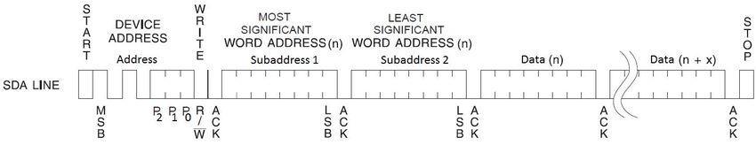
Copyright
© 2017 - 2021 HID Global Corporation/ASSA ABLOY AB. All rights reserved.
This document may not be reproduced, disseminated or republished in any form without the prior written
permission of HID Global Corporation.

Trademarks
HID GLOBAL, HID, the HID Brick logo, the Chain Design and OMNIKEY are trademarks or registered
trademarks of HID Global, ASSA ABLOY AB, or its affiliate(s) in the US and other countries and may not be
used without permission. All other trademarks, service marks, and product or service names are trademarks
or registered trademarks of their respective owners.

Revision history
Date                 Description                                                                    Revision
May 2021             Section 5.2: Modified the line stating the default value.                      A.5
January 2020         Added Automatic PPS (84h) and Card Class Support (85h).                        A.4
July 2018            Update to Section 6.2.                                                         A.3
November 2017        Update to Section 8.1.6.                                                       A.2
April 2017           Update to Section 8.1.9, addition of OMNIKEY 1021.                             A.1
February 2017        Initial Release.                                                               A.0

Contacts
For additional offices around the world, see www.hidglobal.com/contact/corporate-offices

 Americas and Corporate                                             Asia Pacific

 611 Center Ridge Drive                                             19/F 625 King’s Road
 Austin, TX 78753                                                   North Point, Island East
 USA                                                                Hong Kong
 Phone: +1 866 607 7339                                             Phone: +852 3160 9833

 Europe, Middle East and Africa (EMEA)                              Brazil

 3 Cae Gwyrdd                                                       Condomínio Business Center
 Green Meadow Springs                                               Av. Ermano Marchetti, 1435
 Cardiff CF15 7AB                                                   Galpão A2 - CEP 05038-001
 United Kingdom                                                     Lapa - São Paulo / SP, Brazil
 Phone: +44 (0) 1440 711 822                                        Phone: +55 11 5514-7100

 HID Global Technical Support: www.hidglobal.com/support

  2                                                                                                       May 2021
Contents

Section 1: Introduction . . . . . . . . . . . . . . . . . . . . . . . . . . . . . . . . . . . . . . . . . . . . . . . . . . . . . . . . . . . . . . 5
                 1.1      Purpose. . . . . . . . . . . . . . . . . . . . . . . . . . . . . . . . . . . . . . . . . . . . . . . . . . . . . . . . . . . . . . . . . . . . . . . . . 5
                 1.2      Product description . . . . . . . . . . . . . . . . . . . . . . . . . . . . . . . . . . . . . . . . . . . . . . . . . . . . . . . . . . . . . . 5
                 1.3      Key features. . . . . . . . . . . . . . . . . . . . . . . . . . . . . . . . . . . . . . . . . . . . . . . . . . . . . . . . . . . . . . . . . . . . . 5
                 1.4      Reference documents . . . . . . . . . . . . . . . . . . . . . . . . . . . . . . . . . . . . . . . . . . . . . . . . . . . . . . . . . . . . 6
                 1.5      Abbreviations and definitions . . . . . . . . . . . . . . . . . . . . . . . . . . . . . . . . . . . . . . . . . . . . . . . . . . . . . 7
Section 2: Getting started . . . . . . . . . . . . . . . . . . . . . . . . . . . . . . . . . . . . . . . . . . . . . . . . . . . . . . . . . . . 9
                 2.1      Driver installation . . . . . . . . . . . . . . . . . . . . . . . . . . . . . . . . . . . . . . . . . . . . . . . . . . . . . . . . . . . . . . . . 9
                 2.2      HID OMNIKEY® Workbench . . . . . . . . . . . . . . . . . . . . . . . . . . . . . . . . . . . . . . . . . . . . . . . . . . . . . . . 9
Section 3: Host interfaces. . . . . . . . . . . . . . . . . . . . . . . . . . . . . . . . . . . . . . . . . . . . . . . . . . . . . . . . . . . . 11
                 3.1      USB . . . . . . . . . . . . . . . . . . . . . . . . . . . . . . . . . . . . . . . . . . . . . . . . . . . . . . . . . . . . . . . . . . . . . . . . . . . . 11
                       3.1.1     Endpoints assignment . . . . . . . . . . . . . . . . . . . . . . . . . . . . . . . . . . . . . . . . . . . . . . . . . . . . . . . . 11
Section 4: Human interface . . . . . . . . . . . . . . . . . . . . . . . . . . . . . . . . . . . . . . . . . . . . . . . . . . . . . . . . . . 13
                 4.1      LEDs . . . . . . . . . . . . . . . . . . . . . . . . . . . . . . . . . . . . . . . . . . . . . . . . . . . . . . . . . . . . . . . . . . . . . . . . . . 13
Section 5: Contact Card Interface . . . . . . . . . . . . . . . . . . . . . . . . . . . . . . . . . . . . . . . . . . . . . . . . . . . . . 15
                 5.1      Card activation . . . . . . . . . . . . . . . . . . . . . . . . . . . . . . . . . . . . . . . . . . . . . . . . . . . . . . . . . . . . . . . . . 15
                 5.2      Voltage selection . . . . . . . . . . . . . . . . . . . . . . . . . . . . . . . . . . . . . . . . . . . . . . . . . . . . . . . . . . . . . . . 17
                 5.3      Data exchange level. . . . . . . . . . . . . . . . . . . . . . . . . . . . . . . . . . . . . . . . . . . . . . . . . . . . . . . . . . . . . 17
                       5.3.1     TPDU exchange level. . . . . . . . . . . . . . . . . . . . . . . . . . . . . . . . . . . . . . . . . . . . . . . . . . . . . . . . .18
                       5.3.2     APDU exchange level . . . . . . . . . . . . . . . . . . . . . . . . . . . . . . . . . . . . . . . . . . . . . . . . . . . . . . . .18
                       5.3.3     Extended APDU exchange level . . . . . . . . . . . . . . . . . . . . . . . . . . . . . . . . . . . . . . . . . . . . . . .18
                 5.4      Operating mode . . . . . . . . . . . . . . . . . . . . . . . . . . . . . . . . . . . . . . . . . . . . . . . . . . . . . . . . . . . . . . . . 18
                       5.4.1     ISO mode . . . . . . . . . . . . . . . . . . . . . . . . . . . . . . . . . . . . . . . . . . . . . . . . . . . . . . . . . . . . . . . . . . .18
                       5.4.2     EMVCo mode. . . . . . . . . . . . . . . . . . . . . . . . . . . . . . . . . . . . . . . . . . . . . . . . . . . . . . . . . . . . . . . .18
                 5.5      Automatic PPS . . . . . . . . . . . . . . . . . . . . . . . . . . . . . . . . . . . . . . . . . . . . . . . . . . . . . . . . . . . . . . . . . 19
                 5.6      Card class support . . . . . . . . . . . . . . . . . . . . . . . . . . . . . . . . . . . . . . . . . . . . . . . . . . . . . . . . . . . . . . 19
Section 6: Personal Computer / Smart Card . . . . . . . . . . . . . . . . . . . . . . . . . . . . . . . . . . . . . . . . . . . . 21
                 6.1      How to access a smart card or reader through PC/SC . . . . . . . . . . . . . . . . . . . . . . . . . . . . . . 21
                 6.2      Vendor specific commands . . . . . . . . . . . . . . . . . . . . . . . . . . . . . . . . . . . . . . . . . . . . . . . . . . . . . . 23
                       6.2.1     Response APDU . . . . . . . . . . . . . . . . . . . . . . . . . . . . . . . . . . . . . . . . . . . . . . . . . . . . . . . . . . . . 24
                       6.2.2     Error response. . . . . . . . . . . . . . . . . . . . . . . . . . . . . . . . . . . . . . . . . . . . . . . . . . . . . . . . . . . . . . 24

   May 2021                                                                                                                                                                          3
PLT-03099, Rev. A.5

Section 7: Asynchronous cards support. . . . . . . . . . . . . . . . . . . . . . . . . . . . . . . . . . . . . . . . . . . . . . . 27
                7.1    Standard APDU. . . . . . . . . . . . . . . . . . . . . . . . . . . . . . . . . . . . . . . . . . . . . . . . . . . . . . . . . . . . . . . . . 27
                   7.1.1      Command APDU definition . . . . . . . . . . . . . . . . . . . . . . . . . . . . . . . . . . . . . . . . . . . . . . . . . . 27
                   7.1.2      Response APDU definition . . . . . . . . . . . . . . . . . . . . . . . . . . . . . . . . . . . . . . . . . . . . . . . . . . . 27
                7.2    Extended APDU . . . . . . . . . . . . . . . . . . . . . . . . . . . . . . . . . . . . . . . . . . . . . . . . . . . . . . . . . . . . . . . . 28
Section 8: Synchronous cards support . . . . . . . . . . . . . . . . . . . . . . . . . . . . . . . . . . . . . . . . . . . . . . . . 29
                8.1    PC/SC command set . . . . . . . . . . . . . . . . . . . . . . . . . . . . . . . . . . . . . . . . . . . . . . . . . . . . . . . . . . . . 29
                   8.1.1      Read Binary . . . . . . . . . . . . . . . . . . . . . . . . . . . . . . . . . . . . . . . . . . . . . . . . . . . . . . . . . . . . . . . . 30
                   8.1.2      Update Binary . . . . . . . . . . . . . . . . . . . . . . . . . . . . . . . . . . . . . . . . . . . . . . . . . . . . . . . . . . . . . . . 31
                   8.1.3      Verify. . . . . . . . . . . . . . . . . . . . . . . . . . . . . . . . . . . . . . . . . . . . . . . . . . . . . . . . . . . . . . . . . . . . . . 32
                   8.1.4      Read Protection Memory . . . . . . . . . . . . . . . . . . . . . . . . . . . . . . . . . . . . . . . . . . . . . . . . . . . . 33
                   8.1.5      Compare and Protect . . . . . . . . . . . . . . . . . . . . . . . . . . . . . . . . . . . . . . . . . . . . . . . . . . . . . . . 34
                   8.1.6      Modify . . . . . . . . . . . . . . . . . . . . . . . . . . . . . . . . . . . . . . . . . . . . . . . . . . . . . . . . . . . . . . . . . . . . . 35
                   8.1.7      I2C Init. . . . . . . . . . . . . . . . . . . . . . . . . . . . . . . . . . . . . . . . . . . . . . . . . . . . . . . . . . . . . . . . . . . . . 36
                   8.1.8     I2C Write . . . . . . . . . . . . . . . . . . . . . . . . . . . . . . . . . . . . . . . . . . . . . . . . . . . . . . . . . . . . . . . . . . 38
                   8.1.9     I2C Read . . . . . . . . . . . . . . . . . . . . . . . . . . . . . . . . . . . . . . . . . . . . . . . . . . . . . . . . . . . . . . . . . . . 39
                8.2    Vendor-specific synchronous command set . . . . . . . . . . . . . . . . . . . . . . . . . . . . . . . . . . . . . . 40
                   8.2.1     2WBP Read/Write . . . . . . . . . . . . . . . . . . . . . . . . . . . . . . . . . . . . . . . . . . . . . . . . . . . . . . . . . . 40
                   8.2.2     3WBP Read/Write . . . . . . . . . . . . . . . . . . . . . . . . . . . . . . . . . . . . . . . . . . . . . . . . . . . . . . . . . . 42
                   8.2.3     I2C Read/Write . . . . . . . . . . . . . . . . . . . . . . . . . . . . . . . . . . . . . . . . . . . . . . . . . . . . . . . . . . . . . 44
Section 9: Reader configuration . . . . . . . . . . . . . . . . . . . . . . . . . . . . . . . . . . . . . . . . . . . . . . . . . . . . . 49
                9.1    Reader Capabilities . . . . . . . . . . . . . . . . . . . . . . . . . . . . . . . . . . . . . . . . . . . . . . . . . . . . . . . . . . . . 50
                9.2    Contact Slot Configuration. . . . . . . . . . . . . . . . . . . . . . . . . . . . . . . . . . . . . . . . . . . . . . . . . . . . . . . 52
                9.3    User EEPROM area. . . . . . . . . . . . . . . . . . . . . . . . . . . . . . . . . . . . . . . . . . . . . . . . . . . . . . . . . . . . . . 54
                   9.3.1      Write . . . . . . . . . . . . . . . . . . . . . . . . . . . . . . . . . . . . . . . . . . . . . . . . . . . . . . . . . . . . . . . . . . . . . . 54
                   9.3.2      Read . . . . . . . . . . . . . . . . . . . . . . . . . . . . . . . . . . . . . . . . . . . . . . . . . . . . . . . . . . . . . . . . . . . . . . 54
                9.4 Reader Configuration Control . . . . . . . . . . . . . . . . . . . . . . . . . . . . . . . . . . . . . . . . . . . . . . . . . . . . 55
Appendix A: Enabling Escape CCID commands . . . . . . . . . . . . . . . . . . . . . . . . . . . . . . . . . . . . . . . . . 57
Appendix B: Sample code . . . . . . . . . . . . . . . . . . . . . . . . . . . . . . . . . . . . . . . . . . . . . . . . . . . . . . . . . . . 59

  4                                                                                                                                                                May 2021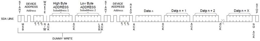
Section            1
1 Introduction

1.1 Purpose
This Software Developer Guide is intended for developers integrating ISO/IEC 7816 contact cards using
OMNIKEY® Contact Smart Card Readers.
The following OMNIKEY readers are covered in this document:
  ■   OMNIKEY 1021
  ■   OMNIKEY 3021
  ■   OMNIKEY 3121
  ■   OMNIKEY 3121 RB
  ■   OMNIKEY 6121
All readers listed are based on the OMNIKEY Contact Smart Card chipset.

1.2 Product description
OMNIKEY Smart Card Readers open new market opportunities for system integrators seeking simple reader
integration and development using standard interfaces, such as CCID (Circuit Card Interface Device). These
readers work without installing or maintaining device drivers, only an operating system driver, for example
Microsoft CCID driver, is necessary.
Features of the OMNIKEY Smart Card Reader include supporting the ISO/IEC 7816-3 card technology as well
as synchronous cards support.

1.3 Key features
  ■   CCID Support – Removes the requirement to install drivers on standard operating systems to fully
      support capabilities of the reader board.
  ■   ISO/IEC 7816-3 – Supports the common contact card technology including synchronous card support.
  ■   Rapid and Easy Integration – No special driver installation is required.
  ■   Advanced Power Management – Supports Low Power modes specified by USB:
      ■ Allows the host device to turn off the reader to save power (while the reader is still able to detect
        cards, with reduced power).
      ■ Allows the reader to wake up the host device.

  May 2021                                                                                                      5
Introduction PLT-03099, Rev. A.5
1.4 Reference documents
Document number Description
CCID Specification Specification for Integrated Circuit(s) Cards Interface Devices. Revision 1.1
ISO 7816-3 Identification cards - Integrated circuit cards - Part 3: Organization, security and
commands for interchange. Third Edition 2016.
ISO 7816-4 Identification cards - Integrated circuit cards - Part 4: Organization, security and
commands for interchange. Second Edition 2005.
ISO 8825 ISO/IEC8825 ASN.1 encoding rules
Specification of Basic Encoding Rules (BER), Canonical Encoding Rules (CER) and
Distinguished Encoding Rules (DER). Fourth Edition 2008
or
X.690
Information technology – ASN.1 encoding rules:
Specification of Basic Encoding Rules (BER), Canonical Encoding Rules (CER) and
Distinguished Encoding Rules (DER).
PCSC-3-Sup-CL Interoperability Specification for ICCs and Personal Computer Systems
Part 3. Supplemental Document for Contactless ICCs
Revision 2.02.00
PCSC-3 Interoperability Specification for ICCs and Personal Computer Systems
Part 3. Requirements for PC-Connected Interface Devices
Revision 2.01.09
PCSC-3-Sup Interoperability Specification for ICCs and Personal Computer Systems
Part 3. Supplemental Document
Revision 2.01.08
PCSC-3-AMD Interoperability Specification for ICCs and Personal Computer Systems
Part 3. Requirements for PC-Connected Interface Devices - AMENDMENT 1
Revision 2.01.09
6 May 2021PLT-03099, Rev. A.5 Introduction 1.5 Abbreviations and definitions Abbreviation Description AES Advanced Encryption Standard APDU Application Protocol Data Unit API Application Programming Interface ASN.1 Abstract Syntax Notation One BER Basic Encoding Rules CLA Class byte of an APDU CSN Card Serial Number DER Distinguished Encoding Rules IFD Interface Device (for accessing ICC card) MAC Message Authentication Code MSDN Microsoft Developer Network OID Object Identifier PAC Physical Access Control PACS PAC Physical Access Control Services PDU Protocol Data Unit PC/SC Personal Computer / Smart Card SIO Secure Identity Object May 2021 7
Introduction                                            PLT-03099, Rev. A.5

                   This page is intentionally left blank.

8                                                                     May 2021
Section 2 2 Getting started 2.1 Driver installation No extra driver installation is necessary and every CCID compliant driver should work with the reader. However, Microsoft’s CCID driver prevents the execution of CCID Escape commands. If an application uses CCID Escape commands these have to be enabled, see Appendix A - Enabling Escape CCID commands. 2.2 HID OMNIKEY® Workbench HID OMNIKEY® Contact Smart Card Readers can be configured using the OMNIKEY Workbench Tool, available from https://www.hidglobal.com/drivers. May 2021 9
Getting started                                       PLT-03099, Rev. A.5

                  This page is intentionally left blank.

10                                                                   May 2021
Section 3 3 Host interfaces 3.1 USB OMNIKEY® Smart Card Readers support USB 2.0 Full Speed (12 Mbit/s) interface. The device enumerates as a single device. USB protocol stack implements the following device class: ■ CCID (Integrated Circuit Cards Interface Device, v1.1) 3.1.1 Endpoints assignment The table below lists the USB protocol stack endpoints, their parameters and functional assignment. Endpoint Description Type Max. packet size EPX Control Endpoint Interrupt IN/OUT EPX Smart Card Bulk OUT EPX Smart Card Bulk IN EPX Smart Card Interrupt IN May 2021 11
Host interfaces                                       PLT-03099, Rev. A.5

                  This page is intentionally left blank.

12                                                                   May 2021
Section 4 4 Human interface 4.1 LEDs The reader is equipped with a single LED / two LEDs to indicate the current status of the smart card reader. The DATA LED is ON when the smart card is powered. The LED is OFF when the smart card is not powered. The LED blinks when the smart card reader transmits or receives any data to/from host computer. Typically, the operating system powers the smart card when it is inserted into the slot. In this case, the DATA LED is ON. After a few seconds, if no application makes use of the smart card, the LED is OFF indicating card power is off. If any application communicates with the smart card, the LED stays ON and blinks to indicate data transmission. The function of this LED cannot be modified. Only blinking parameters, such as frequency or period, may be altered. The LED does not blink during EEPROM read/write operations on FLASH versions of the reader, but does blink on ROM versions of the reader. May 2021 13
Human interface                                      PLT-03099, Rev. A.5

                 This page is intentionally left blank.

14                                                                  May 2021
Section 5
5 Contact Card Interface
OMNIKEY® Smart Card Readers are compliant with the CCID specification. Each product includes the
following functionality:
■ Configurable Voltage Selection
■ Configurable Data Exchange Level: TPDU, APDU, Extended APDU (for T = 1 cards only)
■ Configurable Operation Mode: ISO or EMVCo
5.1 Card activation
Before a card is ready for data exchange it must be properly activated. The following diagram shows the
activation sequence:
1. The card is inserted into a contact slot.
2. The reader chooses the supply voltage and powers up the card.
3. If there is no response from the card another class is selected and the power up sequence is repeated.
The sequence of voltage selection is configurable with the voltageSelection parameter. If the card
responds the response is evaluated.
4. If the card returns valid ATR, the PPS procedure follows (if applicable). If there is no ATR (i.e. some I2C
cards), the state of lines is checked and the fake ATR composed.
5. Finally the reader notifies CCID about the card presence.
May 2021 15Contact Card Interface PLT-03099, Rev. A.5
Card activation
Card Insertion
Apply a class
Select another class
Power Up Card
Card
No answer to
reset
Yes
ATR
No
available?
Yes
Perform PPS
Generate fake ATR
(if applicable)
Notify CCID
Card ready
16 May 2021PLT-03099, Rev. A.5 Contact Card Interface
5.2 Voltage selection
OMNIKEY Smart Card Readers support all classes listed in ISO/IEC 7816-3.
It is possible to set the following voltage sequence during the voltage selection process. This can be used for
a card that supports more than one class or to accelerate activation time.
Voltage selection sequence is encoded in one byte:
Voltage Sequence
82h
Sequence 3 2 1
Bit 7 6 5 4 3 2 1 0
Voltage 0 0 01 - 1.8 V 01 - 1.8 V 01 - 1.8 V
10 - 3 V 10 - 3 V 10 - 3 V
11 - 5 V 11 - 5 V 11 - 5 V
If all bits are 0, automatic voltage selection is set. This means the device driver is responsible for voltage
selection. The Microsoft CCID driver voltage selection sequence is: 5 V, 3 V, 1.8 V. Bits 7 and 6 are ignored and
should be set to 0.
Examples:
1Bh (27dec) = 00011011: 5 V -> 3 V -> 1.8 V
39h (57dec) = 00111001: 1.8 V -> 3 V -> 5 V
The default value is 1Bh (5 V -> 3 V -> 1.8 V) as shown in the example above.
5.3 Data exchange level
OMNIKEY Smart Card Readers support the following protocols as defined in ISO/IEC 7816 -3:
■ T = 0, T = 1
■ S = 8, S = 9, S = 10
The data exchange level can be configured in one of the following ways:
■ TPDU exchange level
■ APDU exchange level
■ Extended APDU exchange level
Exchange level
80h
Value Comments
01h TPDU exchange level
02h APDU exchange level
03h Extended APDU exchange level
May 2021 17Contact Card Interface PLT-03099, Rev. A.5 5.3.1 TPDU exchange level Transmission Protocol Data Unit (TPDU) level of communication is a type of exchange with the host. For TPDU level exchanges, the CCID provides the transportation of the host’s APDU to the ICC’s (Integrated Circuit Card) TPDU. This protocol is described in ISO 7816-3. Note: For synchronous cards the T = 0 protocol is emulated. 5.3.2 APDU exchange level Application Protocol Data Unit (APDU) level of communication is a type of exchange with the host. For APDU level exchanges, the CCID provides the transportation of host’s APDU to the ICC’s (Integrated Circuit Card) TPDU. Two APDU levels are defined, short APDU and extended APDU. APDU commands and responses are defined in ISO 7816-4. 5.3.3 Extended APDU exchange level The extended APDU data exchange is supported for T = 1 cards only. For T = 0 cards the application should use the ENVELOPE command instead. 5.4 Operating mode 5.4.1 ISO mode This is the default mode of operation for smart card readers. It is designated to operate with ISO 7816-4 compatible cards and synchronous cards. 5.4.2 EMVCo mode This mode is suitable to operate with cards that fulfill the EMVCo specification. Compared to ISO Mode: ■ Only 5 V power supply ■ Synchronous cards not supported Operating mode 83h Value Comments 00h ISO/IEC 7816 mode 01h EMVCo mode 18 May 2021
PLT-03099, Rev. A.5                                                Contact Card Interface

5.5 Automatic PPS
OMNIKEY Smart Card Readers support automatic protocol and parameters selection (PPS). Automatic PPS
can be configured in one of the following ways:
  ■   Automatic PPS disabled (default)
  ■   Automatic PPS enabled with protocol T1
  ■   Automatic PPS enabled with protocol T0
Automatic PPS

84h
Value         Comments
00h           Automatic PPS disabled (default). Protocol and parameters selection is done by the driver.
01h           Automatic PPS enabled with protocol T1
02h           Automatic PPS enabled with protocol T0

5.6 Card class support
OMNIKEY Smart Card Readers support automatic handling of the card class. Card class change support can
be configured in one of following ways:
  ■   Card class change support disabled
  ■   Card class change support enabled (default)
Card class support

85h
Value         Comments
00h           Card class change support disabled
01h           Card class change support enabled (default)

  May 2021                                                                                                 19
Contact Card Interface                                PLT-03099, Rev. A.5

                  This page is intentionally left blank.

20                                                                   May 2021
Section 6
6 Personal Computer / Smart Card
OMNIKEY® Smart Card Readers access contact cards through the framework defined in PC/SC. This makes card
integration a straight forward process for any developer who is already familiar with this framework.
The Microsoft Developer Network (MSDN) Library contains valuable information and complete
documentation of the SCard API within the MSDN Platform SDK.
See: http://msdn.microsoft.com/en-us/library/windows/desktop/aa380149(v=vs.85).aspx
6.1 How to access a smart card or reader through PC/SC
The following steps provide a guideline to create your first smart card application using the industry standard,
PC/SC compliant API function calls. The function definitions provided are taken verbatim from the MSDN
Library [MSDNLIB]. For additional descriptions of these and other PC/SC functions provided by the Microsoft
Windows PC/SC smart card components, refer to the MSDN Library.
See: http://msdn.microsoft.com/en-us/library/ms953432.aspx
1. Establish Context
This step initializes the PC/SC API and allocates all resources necessary for a smart card session. The
SCardEstablishContext function establishes the resource manager context (scope) within which
database operations are performed.
LONG SCardEstablishContext( IN DWORD dwScope,
IN LPCVOID pvReserved1,
IN LPCVOID pvReserved2,
OUT LPSCARDCONTEXT phContext);
2. Get Status Change
Checks the status of the reader for card insertion, removal or availability.
The SCardGetStatusChange function blocks execution until the current availability of the cards in a
specific set of readers change. The caller supplies a list of monitored readers and the maximum wait
time (in milliseconds) for an action to occur on one of the listed readers.
LONG SCardGetStatusChange(IN SCARDCONTEXT hContext,
IN DWORD dwTimeout,
IN OUT LPSCARD_READERSTATE rgReaderStates,
IN DWORD cReaders);
May 2021 21Personal Computer / Smart Card PLT-03099, Rev. A.5
3. List Readers
To acquire a list of all PC/SC readers use the SCardListReaders function. Look for HID Global
OMNIKEY Smart Card Reader in the returned list. If multiple Contact Smart Card readers are connected
to your system, they will be enumerated.
Example: HID Global OMNIKEY Smart Card Reader 0, and HID Global OMNIKEY Smart Card Reader 1.
LONG SCardListReaders( IN SCARDCONTEXT hContext,
IN LPCTSTR mszGroups,
OUT LPTSTR mszReaders,
IN OUT LPDWORD pcchReaders);
4. Connect
Connect to the card. The SCardConnect function establishes a connection (using a specific resource
manager context) between the calling application and a smart card contained by a specific reader. If no
card exists in the specified reader, an error is returned.
LONG SCardConnect( IN SCARDCONTEXT hContext,
IN LPCTSTR szReader,
IN DWORD dwShareMode,
IN DWORD dwPreferredProtocols,
OUT LPSCARDHANDLE phCard,
OUT LPDWORD pdwActiveProtocol);
5. Exchange Data and Commands with the Card or the reader
Exchange command and data through APDUs. The SCardTransmit function sends a service request to
the smart card, expecting to receive data back from the card.
LONG SCardTransmit( IN SCARDHANDLE hCard,
IN LPCSCARD_I0_REQUEST pioSendPci,
IN LPCBYTE pbSendBuffer,
IN DWORD cbSendLength,
IN OUT LPSCARD_IO_REQUEST pioRecvPci,
OUT LPBYTE pbRecvBuffer,
IN OUT LPDWORD pcbRecvLength);
Note: The application communicates through SCardControl()in environments where:
■ SCardTransmit() is not allowed without an ICC
■ SCardTransmit() is not allowed for any other reasons
■ Developers prefer the application communicate through SCardControl()
The application retrieves the control code corresponding to FEATURE_CCID_ESC_COMMAND (see part 10,
rev.2.02.07). In case this feature is not returned, the application may try SCARD_CTL_CODE (3500) as a
control code to use.
LONG SCardControl( IN SCARDHANDLE hCard,
IN DWORD dwControlCode,
IN LPCVOID lpInBuffer,
IN DWORD nInBufferSize,
OUT LPVOID lpOutBuffer,
IN DWORD nOutBufferSize,
OUT LPDWORD lpBytesReturned);
22 May 2021PLT-03099, Rev. A.5 Personal Computer / Smart Card
6. Disconnect
It is not necessary to disconnect the card after the completion of all transactions, but it is
recommended. The SCardDisconnect function terminates a connection previously opened between
the calling application and a smart card in the target reader.
LONG SCardDisconnect( IN SCARDHANDLE hCard,
IN DWORD dwDisposition);
7. Release
This step ensures all system resources are released. The SCardReleaseContext function closes an
established resource manager context, freeing any resources allocated under that context.
LONG SCardReleaseContext( IN SCARDCONTEXT hContext);
6.2 Vendor specific commands
Card readers support features outside the specified commands of PC/SC. To allow applications to control
these features a generic command needs to be used. Use of a generic command prevents conflicts of
reserved INS values used by certain card readers. This command allows applications to control device specific
features provided by the reader.
Note: According to ISO-7816-3 standards, INS bytes 6x and 9x are invalid. The reader will pass the commands
without checking the custom instruction. These INS bytes are reserved for SW1.
Command APDU
CLA INS P1 P2 Lc Data field Le
FFh 70h 07h 6Bh xx DER TLV coded PDU xx
(Vendor Payload)
The IFD supports the INS Byte 70h for vendor specific proprietary commands.
P1 and P2 constitute the vendor ID. For OMNIKEY Smart Card Reader products the VID = 076Bh.
The Data Field is constructed as ASN.1 objects/items, whereby every OMNIKEY Smart Card Reader object is
identified by a unique Object Identifier (OID).
OIDs are organized as a leaf tree under an invisible root node. The following table shows the first root nodes.
Vendor command Tag value Vendor payload branch
A2h (constructed) readerInformationApi
BCh (constructed) deviceSpecificCommand
9Dh (primitive) response
BDh (constructed)
9Eh (primitive) errorResponse
The following sub-sections present all OIDs.
May 2021 23Personal Computer / Smart Card PLT-03099, Rev. A.5
6.2.1 Response APDU
For all commands encapsulated in generic 70h APDU, the IFD returns the response frame constructed as
follows.
Data field SW1 SW2
DER TLV coded Response PDU See ISO 7816-4
The two last bytes of the response frame are always return code, SW1SW2.
In cases of an ISO 7816 violation, the return code is according to ISO 7816-4 and the data field may be empty.
In cases of positive processing or internal errors, the IFD returns SW1SW2 = 9000 and the data field is
encapsulated in the response TAG (9Dh or BDh) or error response TAG (9Eh).
The response includes more than one leaf, depending on the request. Each leaf is encapsulated in the leaf tag.
6.2.2 Error response
The error response tag caused by the firmware core is 9Eh (Class Context Specific) + (Primitive) + (1Eh). The
length is two bytes. The first byte is the cycle in which the error occurred and the second byte is the
exception type.
9E 02 xx yy 90 00
Value Description
9Eh Tag = Error Response (0Eh) + (Class Context Specific) + (Primitive)
02h Len = 2
cycle Value byte 1: Cycle in which the error occurred, see Error Cycle
error Value byte 2: Error code, see Error Code
SW1 90
SW2 00
Error cycle
First value byte
Cycle Description
0 HID Proprietary Command APDU
1 HID Proprietary Response APDU
2 HID Read or Write EEPROM Structure
3 RFU
4 RFU
5 RFU
24 May 2021PLT-03099, Rev. A.5 Personal Computer / Smart Card
Error code
Second value byte
Exception Description
3 03h NOT_SUPPORTED
4 04h TLV_NOT_FOUND
5 05h TLV_MALFORMED
6 06h ISO_EXCEPTION
11 0Bh PERSISTENT_TRANSACTION_ERROR
12 0Ch PERSISTENT_WRITE_ERROR
13 0Dh OUT_OF_PERSISTENT_MEMORY
15 0Fh PERSISTENT_MEMORY_OBJECT_NOT_FOUND
17 11h INVALID_STORE_OPERATION
19 13h TLV_INVALID_STRENGTH
20 14h TLV_INSUFFICIENT_BUFFER
21 15h DATA_OBJECT_READONLY
31 1F APPLICATION_EXCEPTION (Destination Node ID mismatch)
42 2Ah MEDIA_TRANSMIT_EXCEPTION (Destination Node ID mismatch)
43 2Bh SAM_INSUFFICIENT_MSGHEADER (Secure Channel ID not allowed)
47 2Fh TLV_INVALID_INDEX
48 30h SECURITY_STATUS_NOT_SATISFIED
49 31h TLV_INVALID_VALUE
50 32h TLV_INVALID_TREE
64 40h RANDOM_INVALID
65 41h OBJECT_NOT_FOUND
May 2021 25Personal Computer / Smart Card PLT-03099, Rev. A.5
This page is intentionally left blank.
26 May 2021Section 7 7 Asynchronous cards support Asynchronous cards contain a CPU or are memory cards that are accessed through ISO7816-4 compliant framed APDU commands. This type of card supports at least one of the asynchronous protocols T=0 or T=1. No additional libraries or third-party software components are necessary to integrate contactless CPU cards. There is no standard list of APDUs (except those specified in PCSC-3). Typically a card has its own list of unique commands. Consult the specific card specification for full list of supported commands. 7.1 Standard APDU Standard APDU is the application data unit that allows a maximum of 255 bytes of data to be sent to the card. It is supported by all ISO7816-4 compatible cards. 7.1.1 Command APDU definition Command APDU is sent by the reader to the card. It contains a mandatory four byte header and from 0 to 255 bytes of data. CLA INS P1 P2 Lc Command Data Le CLA - Instruction class INS - Instruction code P1, P2 - Command parameters Lc - Number of command data bytes of data Command Data - Lc number bytes of data Le - Maximum number of expected response bytes If Le is omitted, any number of bytes in response is accepted. If Le=0, the reader does not expect any response data (except 2 status bytes SW1, SW2). If the length of command data is 0, Lc must be omitted. 7.1.2 Response APDU definition Response APDU is sent by the card to the reader. It contains from 0 to 255 bytes of data and two mandatory status bytes SW1 and SW2. Command Data SW1 SW2 May 2021 27
Asynchronous cards support                                         PLT-03099, Rev. A.5

7.2 Extended APDU
Extended APDU is an extension to the standard APDU. It allows for more than 255 bytes of data to be
transmitted in command and response. Extended APDU is backward compatible with Standard APDU.
Command and response APDU look exactly the same for both types if the data length is equal or less than
255 bytes.
To use extended APDU the card must support it and the reader must operate in Extended APDU mode. For
additional information on how to enable this mode, see Section 5.3.3 Extended APDU exchange level.
The only difference between Standard APDU and Extended APDU is the length of the Lc and Le fields. In
Extended APDU these may be omitted, 1 or 3 bytes depending of the length of data.
If the length of command data is less or equal to 255 the same rules apply to Lc as for Standard APDU. If the
length of data is greater than 255, Lc must be 3 bytes in length with the first byte equal to 0 and the two
following bytes encoding actual command data length.
Similar rules apply to Le. It may be omitted or 1 byte in the same way as for Standard APDU. If more than 255
bytes of data is expected, it may be 2 bytes long if Lc indicates extended length or 3 bytes long with first byte
equal to 0 if there is no Lc field or Lc indicates length less than 256 bytes (Standard APDU).
For more detailed description of data length encoding rules, please see ISO7816-4.

  28                                                                                                   May 2021
Section         8
8 Synchronous cards support
The device provides two ways to access synchronous cards. One option is PC/SC, a command set that uses
standard APDU syntax and standard SCardTransmit() API, but uses the reserved value of the CLA byte of
‘FF’. The other is through Vendor Specific proprietary synchronous API.

8.1 PC/SC command set
The following are supported through PC/SC.

Command                                             Comments
READ_BINARY                                         Implemented according to PC/SC spec
UPDATE_BINARY                                       Implemented according to PC/SC spec
VERIFY                                              Implemented according to PC/SC spec
READ_PROTECTION_MEMORY                              Proprietary extension to PC/SC
                                                    Applicable for SLE 4418/28/32/42
COMPARE_AND_PROTECT                                 Proprietary extension to PC/SC
                                                    Applicable for SLE 4418/28/32/42
MODIFY                                              Proprietary extension to PC/SC
                                                    Applicable for SLE 4418/28/32/42
I2C_INIT                                            Proprietary extension to PC/SC
                                                    Applicable for I2C cards
I2C_WRITE                                           Proprietary extension to PC/SC
                                                    Applicable for I2C cards
I2C_READ                                            Proprietary extension to PC/SC
                                                    Applicable for I2C cards

  May 2021                                                                                          29
Synchronous cards support PLT-03099, Rev. A.5
8.1.1 Read Binary
This function reads data from the synchronous smart card. If the Le field is set to ‘00’, then all bytes, until the
end of the file, is read within the limit of 256 for a short Le field.
Read Binary Command
CLA INS P1 P2 Lc Data In Le
FFh B0h Address MSB Address LSB — — xx
Note: Read Binary Extended Command with the first byte of the Le field equal to 0x00 is not supported.
Read Binary Output
Data Out
Data + SW1 SW2
Read Binary Error Codes
SW1 SW2 Meaning
Warning 62h 81h Part of returned data may be corrupted
82h End of file reached before reading expected number of bytes
Error 69h 81h Command incompatible
82h Security status not satisfied (no PIN presented)
86h Command not allowed
6Ah 81h Function not supported
82h File not found / Addressed block or byte does not exist
6Ch xxh Wrong length (wrong number Le; ‘xx’ is the exact number)
30 May 2021PLT-03099, Rev. A.5 Synchronous cards support
8.1.2 Update Binary
This function writes data on the synchronous smart card. If the Lc field is set to ‘00’, then 256 bytes, until the
end of the file, is written for a short Lc field.
Update Binary Command
CLA INS P1 P2 Lc Data In Le
FFh D6h Address MSB Address LSB xx Data —
Note: Update Binary Extended Command with first byte of the Le field equal to 0x00 is not supported.
Update Binary Output
Data Out
SW1 SW2
Update Binary Error Codes
SW1 SW2 Meaning
Warning 62h 81h Part of returned data may be corrupted
82h End of file reached before reading expected number of bytes
Error 65h 81h Memory failure (unsuccessful writing)
69h 81h Command incompatible
82h Security status not satisfied (no PIN presented)
86h Command not allowed
6Ah 81h Function not supported
82h File not found / Addressed block or byte does not exist
May 2021 31Synchronous cards support PLT-03099, Rev. A.5
8.1.3 Verify
For some synchronous cards (SLE 4428/42) a security code logic exists which controls the write/erase
access to the memory.
SLE 4442 contains a 4-byte security memory with an Error Counter EC (bit 0 to bit 2) and 3 bytes reference
data (PIN).
SLE 4428 contains a 3 byte security memory with Error Counter EC and 2 bytes reference data (PIN).
After power on, the whole memory, except for the reference data (PIN), is read only. Once a successful
comparison of verification data with the internal reference data has taken place the memory will have full
access functionality (read/write/erase) until power is switched off.
The value of the Error Counter determines the number of possible attempts to verify PIN code. For SLE 4428
there are a maximum of 8 tries, for SLE 4442 there are a maximum of 3 tries.
Verify Command
CLA INS P1 P2 Lc Data In Le
FFh 20h 00h 00h PIN Length PIN —
Note: Verify Extended Command with first byte of the Le field equal to 0x00 is not supported.
Verify Output
Data Out
SW1 SW2
Verify Error Codes
SW1 SW2 Meaning
Warning 63h 00h No information is given
CXh Counter (verification failed; 'X' encodes the number of further
allowed retries)
Error 65h 81h Memory failure (unsuccessful writing)
69h 82h Security status not satisfied
83h Verify method blocked
84h Reference data not usable
6Ah 88h Unknown / not supported Card-Protocol
32 May 2021PLT-03099, Rev. A.5 Synchronous cards support
8.1.4 Read Protection Memory
For each byte of some synchronous cards (SLE 4418/28/32/42) a protection bit exists. This bit should be
retrievable for applications.
Read Protection Memory Command
CLA INS P1 P2 Lc Data In Le
FFh 3Ah Address MSB Address LSB — — xx
Each bit of the protection memory is returned in one complete byte and occupies bit 0. Bit 1–7 are RFU and
set 0x00.
For the sequence of the protection bits LSB coding is used.
Note: Read Protection Memory Extended Command with first byte of the Le field equal to 0x00 is not
supported.
Read Protection Memory Output
Data Out
Data + SW1 SW2
0x00: Protection bit is not set
0x01: Protection bit is set
Read Protection Memory Error Codes
SW1 SW2 Meaning
Warning 62h 81h End of file reached before reading expected number of bytes
Error 69h 81h Command incompatible
82h Security status not satisfied (no PIN presented)
86h Command not allowed
6Ah 81h Function not supported
82h File not found / Addressed block or byte does not exist
6Fh 00h Unknown / not supported Card-Protocol
May 2021 33Synchronous cards support PLT-03099, Rev. A.5
8.1.5 Compare and Protect
For each byte of some synchronous cards (SLE 4418/28/32/42) a protection bit exists. This command
compares the data with the memory and sets the protection bit if the data matches with the memory and the
protection bit is not set for this data byte.
SLE 4432/42 has a special protection memory. In this case the function only compares data in the protection
memory.
Compare and Protect Command
CLA INS P1 P2 Lc Data In Le
FFh 30h 00h 03h 5+N See Data In - field buildup table —
Note: Compare and Protect Extended Command with first byte of the Lc field equal to 0x00 is not
supported.
Data In - field buildup
Version Flag 1 Flag 2 Address Address Data to Compare
01h 00h 00h MSB LSB N Data-Bytes
Compare and Protect Output
Data Out
(Address MSB LSB) + SW1 SW2
The address is only returned if an error occurred while comparing the data bytes.
Compare and Protect Error Codes
SW1 SW2 Meaning
Warning 62h 82h End of file reached before reading expected number of bytes
Error 69h 81h Command incompatible
82h Security status not satisfied (no PIN presented)
86h Command not allowed
6Ah 81h Function not supported
82h File not found / Addressed block or byte does not exist
6Fh 00h Unknown / not supported Card-Protocol
34 May 2021PLT-03099, Rev. A.5 Synchronous cards support
8.1.6 Modify
Synchronous cards such as SLE 4418/28/32/42 provide functionality to change the current PIN.
Modify Command
CLA INS P1 P2 Lc Data In Le
FFh 21h 00h 00h Old PIN + New PIN Length Old PIN + New PIN —
Note: Old PIN + New PIN always needed for correct Modify execution.
Modify Output
Data Out
SW1 SW2
Modify Error Codes
SW1 SW2 Meaning
Warning 63h 00h No information given
CXh Counter (verification failed; ‘X’ encodes the number of further allowed
retries)
Error 65h 81h Memory failure (unsuccessful writing)
69h 82h Security status not satisfied
83h Verify method blocked
6Fh 00h Unknown / not supported Card-Protocol.
Old PIN and New PIN are the same.
May 2021 35Synchronous cards support PLT-03099, Rev. A.5
8.1.7 I2C Init
This command initializes an I2C card with parameters such as Page size, Number of Address Bytes and
Memory size. Predefined card types can be called with the Type - byte. If the Type - byte is zero, their own
parameters will be taken if they are valid.
I2C Command
CLA INS P1 P2 Lc Data In Le
FFh 30h 00h 04h 08h See Data In - field buildup table —
Data In - field buildup
Version Type Page size Number of address bytes Memory size
(1 byte) (1 byte) (1 byte) (1 byte) (4 bytes, MSB first)
01h See Type - definitions table
Type - definitions
Type Page Size Number of Memory size Card
address bytes
00h XX XX MSB XX XX LSB undefined
01h 8 1 256 ST14C02C
02h 8 1 512 ST14C04C
03h 32 2 4096 ST14E32
04h 16 1 512 M14C04
05h 16 1 2048 M14C16
06h 32 2 4096 M14C32
07h 32 2 8192 M14C64
08h 64 2 16384 M14128
09h 64 2 32768 M14256
0Ah 8 1 256 GFM2K
0Bh 16 1 512 GFM4K
0Ch 32 2 4096 GFM32K
0Dh 8 1 128 AT24C01A
0Eh 8 1 256 AT24C02
0Fh 16 1 512 AT24C04
10h 16 1 1024 AT24C08
11h 16 1 2048 AT24C16
12h 16 1 2048 AT24C164
13h 32 2 4096 AT24C32
14h 32 2 8192 AT24C64
15h 64 2 16384 AT24C128
16h 64 2 32768 AT24C256
36 May 2021PLT-03099, Rev. A.5 Synchronous cards support
Type Page Size Number of Memory size Card
address bytes
17h 64 2 16384 AT24CS128
18h 64 2 32768 AT24CS256
19h 128 2 65536 AT24C512
1Ah 0 (=256) 2 131072 AT24C1024
1Bh 4 1 256 X24026
2IC Init Output
Data Out
SW1 SW2
I2C Init Error Codes
SW1 SW2 Meaning
Warning 63h 00h No information given
Error 69h 86h Command not allowed (wrong parameters)
6Ah 81h Function not supported
6Fh 00h Unknown / not supported Card-Protocol
May 2021 37Synchronous cards support PLT-03099, Rev. A.5
8.1.8 I2C Write
This command writes data on the I2C card. The command can only write to a maximum of 250 bytes at once.
I2C Write Command
CLA INS P1 P2 Lc Data In Le
FFh 30h 00h 06h 5+N See Data In - field buildup table —
The Lc field contains the number of Data-Bytes to write. 5 Bytes need to be added because of the 5
Byte-Header.
Note: I2C Write Extended Command with first byte of the Lc field equal to 0x00 is not supported.
Data In - field buildup
Version Address bytes Data
(1 byte) (4 bytes, MSB first) (0 - 250 bytes)
01h MSB XX XX LSB Data to write
I2C Write Output
Data Out
SW1 SW2
I2C Write Error Codes
SW1 SW2 Meaning
Warning 62h 82h End of file reached before reading expected number of bytes
Error 69h 81h Command incompatible
86h Command not allowed
6Ah 81h Function not supported
82h File not found / Addressed block or byte does not exist
6Fh 00h Unknown / not supported Card-Protocol
38 May 2021PLT-03099, Rev. A.5 Synchronous cards support
8.1.9 I2C Read
This command reads the content from the I2C card.
I2C Read Command
CLA INS P1 P2 Lc Data In Le
FFh 30h 00h 05h 09h See Data In - field buildup table —
Data In-Field Buildup
Version Address bytes Length
(1 byte) (4 bytes, MSB first) (4 bytes, MSB first)
01h MSB XX XX LSB MSB XX XX LSB1
1 Maximum length value is 0x000000FD (253).
I2C Read Output
Data Out
Data + SW1 SW2
I2C Read Error Codes
SW1 SW2 Meaning
Warning 62h 82h End of file reached before reading expected number of bytes
Error 69h 81h Command incompatible
86h Command not allowed
6Ah 81h Function not supported
82h File not found / Addressed block or byte does not exist
6Fh 00h Unknown Protocol / Memory Allocation failure
May 2021 39Synchronous cards support PLT-03099, Rev. A.5
8.2 Vendor-specific synchronous command set
These commands allow applications to communicate with synchronous contact cards using raw native card
commands directly sent to the card by the Bus Protocol.
All synchronous contact card commands are identified by a unique ASN.1 leaf. The root is defined as a
Synchronous Card Command and is encapsulated in vendor specific generic command. Under this root are
specific commands for 2WBP (2 Wire Bus Protocol), 3WBP (3 Wire Bus Protocol) and I2C cards, organized as
follows.
Synchronous Card Command Structure
Vendor command Tag value Native card command
A6h (constructed) 2WBPReaderWrite [A0h]
3WBPReaderWrite [A1h]
I2CReaderWrite [A0h]
8.2.1 2WBP Read/Write
This command allows communication with a synchronous contact smart card that supports a 2 Wire Bus
Protocol (2WBP) such as SLE 4432/42.
Each command consists of three bytes:
■ Control
■ Address
■ Data
For SLE 4432 there are four commands available. These are listed in the table below.
2WBP Common Commands
Byte 1 Byte 2 Byte 3 Command
Control Address Data
B7 B6 B5 B4 B3 B2 B1 B0 A7 - A0 D7 - D0
0 0 1 1 0 0 0 0 address no effect Read Main Memory
0 0 1 1 1 0 0 0 address input data Update Main Memory
0 0 1 1 0 1 0 0 no effect no effect Read Protection Memory
0 0 1 1 1 1 0 0 address input data Write Protection Memory
In addition to the above commands there are three commands available for the SLE 4442. These are listed in
the table below.
2WBP SLE 4442 only Commands
Byte 1 Byte 2 Byte 3 Command
Control Address Data
B7 B6 B5 B4 B3 B2 B1 B0 A7 - A0 D7 - D0
0 0 1 1 0 0 0 1 no effect no effect Read Security Memory
0 0 1 1 1 0 0 1 address input data Update Security Memory
0 0 1 1 0 0 1 1 address input data Compare Verification Data
40 May 2021PLT-03099, Rev. A.5 Synchronous cards support
More information can be found in ICs for Chip Cards Intelligent 256-Byte EEPROM SLE 4432/SLE 4442
datasheet prepared by SIEMENS.
Example Update Main Memory
Command:
FF 70 07 6B 07 //Vendor Specific APDU with 7 bytes object
A6 05 //Synchronous Card Command
A0 03 //2WBPReadWrite
38 AA 55 //Control = 0x38, Address = 0xAA, Data = 0x55
00 //Le
Reply:
BD 02 //Response
A0 00 //Received data (0 bytes)
99 00 //SW1SW2
Example Read Main Memory
Command:
FF 70 07 6B 07 //Vendor Specific APDU with 7 bytes object
A6 05 //Synchronous Card Command
A0 03 //2WBPReadWrite
30 AA 00 //Control = 0x30, Address = 0xAA, Data = 0x00
00 //Le
Reply:
BD 03 //Response
A0 01 //Received data (1 byte)
55 //Data
99 00 //SW1SW2
May 2021 41Synchronous cards support PLT-03099, Rev. A.5
8.2.2 3WBP Read/Write
This command allows communication with a synchronous contact smart card that supports a 3 Wire Bus
Protocol (3WBP) such as SLE 4418/28.
Each command consists of three bytes.
3WBP Control Words for Commands Entry
Byte 1 Byte 2 Byte 3 Command
A9 A8 S5 S4 S3 S2 S1 S0 A7 - A0 D7 - D0
1 1 0 0 0 1 input data Write and erase with protect
bit
1 1 0 0 1 1 input data Write and erase without
protect bit
1 1 0 0 0 0 comparison Write protect bit with data
address address data comparison (verification)
bit bit
0 0 1 1 0 0 no effect Read 9 bits, data with protect
9 and 0 7-0
bit
0 0 1 1 1 0 no effect Read 8 bits, data without
protect bit
1 1 0 0 0 1 input data Write and erase with protect
bit
3WBP SLE 4442 only Commands
Byte 1 Byte 2 Byte 3 Command
A9 A8 S5 S4 S3 S2 S1 S0 A7 - A0 D7 - D0
1 1 1 1 0 0 1 0 0xFD bit mask Write error counter
1 1 0 0 1 1 0 1 0xFE PIN byte 1 Verify first PIN byte
1 1 0 0 1 1 0 1 0xFF PIN byte 2 Verify second PIN byte
More information can be found in ICs for Chip Cards SLE 4418/SLE 4428 Intelligent 8-Kbit EEPROM datasheet
prepared by SIEMENS.
42 May 2021PLT-03099, Rev. A.5 Synchronous cards support
Example Read Memory with Protect Bit
Command:
FF 70 07 6B 07 //Vendor Specific APDU with 7 bytes object
A6 05 //Synchronous Card Command
A1 03 //3WBPReadWrite
0C AA 00 //Address = 0xAA
00 //Le
Reply:
BD 04 //Response
A1 02 //Received data (2 bytes)
AA 80 //Data = 0xAA, Protect bit = 0x80 (set)
90 00 //SW1SW2
Example Write Memory without Protect Bit
Command:
FF 70 07 6B 07 //Vendor Specific APDU with 7 bytes object
A6 05 //Synchronous Card Command
A1 03 //3WBPReadWrite
33 AA BB //Address = 0xAA, Data = 0xBB
00 //Le
Reply:
BD 02 //Response
A1 00 //Received data (0 bytes)
90 00 //SW1SW2
May 2021 43Synchronous cards support PLT-03099, Rev. A.5
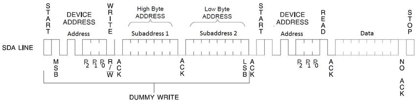
8.2.3 I2C Read/Write
This command allows communication with a synchronous contact smart card that supports a I2C Bus
Protocol such as AT24C01/02/04/…/1024 etc.
Each command consists of 5+N bytes.
I2C Read/Write Command
Offset Field Size Value Description
0 Address length 1 1, 2, 3 length of address:
1…salve address only
2…slave address + byte-subaddress
3…slave address + word-subaddress
1 Bytes to read/write 1 N # of bytes to read/write
2 Address 1 device address
3 Subaddress 1 1 First byte of subaddress
4 Subaddress 2 1 Second byte of subaddress
5 Data N array of data bytes
Note: 32 bytes is the maximum value of “Bytes to read/write” field.
The device address word consists of a mandatory one, zero sequence for the first four most significant bits as
shown. This is common to all I2C EEPROM devices.
I2C Device Address
1 0 1 0 P2 P1 P0 R/W
MSB LSB
The next 3 bits are used for memory page addressing. These page addressing bits should be considered the
most significant bits of the data word address.
More information about I2C EEPROM memory addressing, can be found in datasheets of “Two-wire serial
EEPROM” prepared by Atmel, for example, AT24C01 or AT24C1024.
I2C Byte Read Command
44 May 2021PLT-03099, Rev. A.5 Synchronous cards support I2C N-Byte Read Command The correct synchronous contact smart card documentation should be checked to determine how big the address length is. For some Smart Cards, such as AT24C01, 2 bytes sub-address is not necessary. I2C Byte Write Command I2C N-Byte Write Command The N-Byte Write command can write a maximum of 32 bytes at once, however when the internally generated word address (inside the Smart Card EEPROM memory), reaches the page boundary, the following byte is placed at the beginning of the same page. The address “rollover” during write is from the last byte of the current page to the first byte of the same page. The correct synchronous contact smart card documentation should be checked to determine how big the memory page is. May 2021 45
Synchronous cards support                              PLT-03099, Rev. A.5

Example Read 16 bytes, address 0x0100 (AT24C1024, 3 bytes of address length)
Command:
FF 70 07 6B 09                          //Vendor Specific APDU with 9 bytes object
   A6 07                                //Synchronous Card Command
         A2 05                          //I2CReadWrite
              03 10 A1 01 00            //5 bytes of command
                 00                     //Le
Reply:
BD 12                                   //Response
   A2 10                                //Received data (16 bytes)
         16 Bytes of received data      //Data
              90 00                     //SW1SW2

Example Read 8 bytes, address 0x05 (AT24C01, 2 bytes of address length)
Command:
FF 70 07 6B 09                         //Vendor Specific APDU with 9 bytes object
   A6 07                               //Synchronous Card Command
         A2 05                         //I2CReadWrite
              02 08 A1 50 00           //5 bytes of command
                 00                    //Le
Reply:
BD 0A                                  //Response
   A2 08                               //Received data (8 bytes)
         8 Bytes of received data      //Data
              90 00                    //SW1SW2

Example Read 1 byte, current address (1 byte of address length)
Command:
FF 70 07 6B 09                         //Vendor Specific APDU with 9 bytes object
   A6 07                               //Synchronous Card Command
         A2 05                         //I2CReadWrite
              01 01 A1 00 00           //5 bytes of command
                 00                    //Le
Reply:
BD 03                                  //Response
   A2 01                               //Received data (0 bytes)
         XX                            //Data
              90 00                    //SW1SW2

  46                                                                                      May 2021
PLT-03099, Rev. A.5 Synchronous cards support
Example Write 8 bytes, address 0x0100 (AT24C1024, 3 bytes of address length)
Command:
FF 70 07 6B 11 //Vendor Specific APDU with 9 bytes object
A6 0F //Synchronous Card Command
A2 0D //I2CReadWrite
03 08 A0 01 00 //5 bytes of command
XX XX XX XX XX XX XX XX //Data to write
00 //Le
Reply:
BD 02 //Response
A2 00 //Received data (0 bytes)
90 00 //SW1SW2
May 2021 47Synchronous cards support PLT-03099, Rev. A.5
This page is intentionally left blank.
48 May 2021Section 9
9 Reader configuration
All OMNIKEY® Smart Card Reader configuration items are identified by a unique ASN.1 leaf. The root is defined
as Reader Information API and is encapsulated in a proprietary command, see Section 6.2 Vendor specific
commands.
The root tag readerInformationApi A2h is reserved for GET and SET of reader specific information and
provides access to reader configuration.
For a Reader Information GET requests the Le byte must be present, and the Response Tag (1D) is always
CONSTRUCTED.
Under the root and the GET/SET request are a number of branches, organized as follows:
Reader Information Structure
Vendor command Reader information API Request ASN1 name of branches
FF 70 07 6B Lc Tag = A2h Get [A0h] readerCapabilities [A0h] (read only)
Set [A1H] tlvVersion [80h]
deviceID [81h]
product Name [82h]
product Platform [83h]
firmwareVersion [85h]
hardwareVersion [89h]
hostInterfaces [8Ah]
numberOfContactSlots [8Bh]
vendorName [8Fh]
exchangeLevel [91h]
serialNumber [92h]
sizeOfUserEERrom [94h]
firmwareLabel [96]
contactSlotConfiguration [A3h]
exchangeLevel [91h]
voltageSequence [82h]
operatingMode [83h]
automaticPPS [84h]
cardClassSupport [85h]
readerEEPROM [A7h]
eepromOffset [81h]
eepromRdLength [82h]
eepromWrData [83h]
readerConfigurationControl [A9h] (write only)
rebootDevice [80h]
restoreFactoryDefaults [81h]
Note: After SET requests, restart the reader to apply the changes.
May 2021 49Reader configuration PLT-03099, Rev. A.5 9.1 Reader Capabilities The tag readerCapabilities A0h is constructed. One or more primitive sub tags must follow. Tag ASN.1 name Value Type Len Access TLV Version 80h tlvVersion 01h Uint8_t 1 RO Get APDU: FF 70 07 6B 08 A2 06 A0 04 A0 02 80 00 00 Response: BD 03 80 01 01 90 00 Device ID 81h deviceID 00h 04h Octet String 2 RO Get APDU: FF 70 07 6B 08 A2 06 A0 04 A0 02 81 00 00 Response: BD 04 81 02 00 04 90 00 Name of product 82h productName 3121SC Null String 11 RO Get APDU: FF 70 07 6B 08 A2 06 A0 04 A0 02 82 00 00 Response: BD 0A 82 08 33 31 32 31 20 53 43 00 90 00 Name of processor platform 83h productPlatform AViatoR Null String 8 RO Get APDU: FF 70 07 6B 08 A2 06 A0 04 A0 02 83 00 00 Response: BD 0A 83 08 41 56 69 61 74 6F 52 00 90 00 FwVersionMajor + FwVersionMinor + RevisionNr 85h firmwareVersion 01h 00h 01h Octet String 3 RO Get APDU: FF 70 07 6B 08 A2 06 A0 04 A0 02 85 00 00 Response: BD 05 85 03 01 00 01 90 00 Hardware Version 89h hardwareVersion PCB-00100 REV2 Null String 16 RO Get APDU: FF 70 07 6B 08 A2 06 A0 04 A0 02 89 00 00 Response: BD 11 89 0F 50 43 42 2D 30 30 31 30 30 20 52 45 56 32 00 90 00 Available host communication interfaces, bit 1 = USB 8A hostInterfaces 02h Null String 1 RO Get APDU: FF 70 07 6B 08 A2 06 A0 04 A0 02 8A 00 00 Response: BD 03 8A 01 02 90 00 Number of available contact slots 8Bh numberOfContactSlots 01h Uint8_t 1 RO Get APDU: FF 70 07 6B 08 A2 06 A0 04 A0 02 8B 00 00 Response: BD 03 8B 01 01 90 00 Vendor name 8Fh vendorName HID Global Null String 7 RO Get APDU: FF 70 07 6B 08 A2 06 A0 04 A0 02 8F 00 00 Response: BD 0D 8F 0B 48 49 44 20 47 6C 6F 62 61 6C 00 90 00 50 May 2021
PLT-03099, Rev. A.5                                                  Reader configuration

Tag             ASN.1 name                      Value                  Type              Len          Access
Exchange Level
91h             exchangeLevel                   02h                    Uint8_t           1            RO
Get APDU: FF 70 07 6B 08 A2 06 A0 04 A0 02 91 00 00
Response: BD 0D 91 01 02 90 00
Serial number
92h             serialNumber                    (empty number)         Octet String      0            RO
Get APDU: FF 70 07 6B 08 A2 06 A0 04 A0 02 92 00 00
Response: BD 12 92 00 90 00
Size of user EEProm
94h             sizeOfUserEEProm                04h 00h                Octet String      2            RO
Get APDU: FF 70 07 6B 08 A2 06 A0 04 A0 02 94 00 00
Response: BD 12 94 02 04 00 90 00
Firmware build information
96h             firmwareLabel                   AVRCC-1.2.0148-2015    Octet String      52           RO
                                                0123T100644-EE969
                                                F368D85-FLASH
Get APDU: FF 70 07 6B 08 A2 06 A0 04 A0 02 96 00 00
Response: BD 34 96 32 41 56 52 43 43 2D 31 2E 32 2E 30 2E 31 34 38 2D 32 30 31 35 30 31 32 33 54 31 30 30 36 34 34
2D 45 45 39 36 39 46 33 36 38 44 38 35 2D 46 4C 41 53 48 90 00

 May 2021                                                                                                      51
Reader configuration PLT-03099, Rev. A.5
9.2 Contact Slot Configuration
The following tags can be used to configure contact slot in the contactSlotConfiguration A3h branch.
Tag ASN.1 name Function Len Access
80h exchangeLevel Exchange level: 1 RW
01h - TPDU
02h - APDU
04h - Extended APDU
Set APDU: FF 70 07 6B 0B A2 09 A1 07 A3 05 A0 03 80 01 xx 00
Response: 9D 00 90 00
Get APDU: FF 70 07 6B 0A A2 08 A0 06 A3 04 A0 02 80 00 00
Response: BD 03 80 01 xx 90 00
Tag ASN.1 name Function Len Access
82h voltageSequence Set voltage sequence 1 RW
Set APDU: FF 70 07 6B 0B A2 09 A1 07 A3 05 A0 03 82 01 xx 00
Response: 9D 00 90 00
Get APDU: FF 70 07 6B 0A A2 08 A0 06 A3 04 A0 02 82 00 00
Response: BD 03 82 01 xx 90 00
The sequence encoding byte is described in Section 5.2 Voltage selection.
Tag ASN.1 name Function Len Access
83h operatingMode Operating mode: 1 RW
00h - ISO/IEC 7816 mode
01h - EMVCo modes
Set APDU: FF 70 07 6B 0B A2 09 A1 07 A3 05 A0 03 83 01 xx 00
Response: 9D 00 90 00
Get APDU: FF 70 07 6B 0A A2 08 A0 06 A3 04 A0 02 83 00 00
Response: BD 03 83 01 xx 90 00
The sequence encoding byte is described in Section 5.2 Voltage selection.
Tag ASN.1 name Function Len Access
84h automaticPPS Automatic PPS: 1 RW
00h - Driver control
01h - Protocol T1
02h - Protocol T0
Set APDU: FF 70 07 6B 0B A2 09 A1 07 A3 05 A0 03 84 01 xx 00
Response: 9D 00 90 00
Get APDU: FF 70 07 6B 0A A2 08 A0 06 A3 04 A0 02 84 00 00
Response: BD 03 84 01 xx 90 00
52 May 2021PLT-03099, Rev. A.5 Reader configuration
Tag ASN.1 name Function Len Access
85h cardClassSupport Card class support: 1 RW
00h - Support disabled
01h - Support enabled
Set APDU: FF 70 07 6B 0B A2 09 A1 07 A3 05 A0 03 85 01 xx 00
Response: BD 00 90 00
Get APDU: FF 70 07 6B 0A A2 08 A0 06 A3 04 A0 02 85 00 00
Response: BD 03 85 01 xx 90 00
May 2021 53Reader configuration PLT-03099, Rev. A.5 9.3 User EEPROM area The OMNIKEY Smart Card Reader offers 1024 bytes of EEPROM available for the user. This space may be used to store customer configuration data. There are three tags to use when accessing user EEPROM in the readerEEPROM A7h branch. Tag ASN.1 name Function Len Access 81h eepromOffset Offset on read or write operation 2 RW 82h eepromRdLength Number of bytes to read from offset 1 R 83h eepromWrData Data to write on offset in EEPROM n W When specifying a command to read or write data the eepromOffset tag must be specified. Command to store data in user EEPROM area. 9.3.1 Write Sample command to write 5 bytes at offset 0. Tags Function FF 70 07 6B 11 vendor command A2 0F reader information API A1 0D SET A7 0B readerEEPROM 81 02 00 00 offset 0000 83 05 01 02 03 04 05 00 5 bytes of data Write: FF 70 07 6B 11 A2 0F A1 0D A7 0B 81 02 00 00 83 05 01 02 03 04 05 00 Response: 9D 00 90 00 9.3.2 Read Sample command to read 5 bytes of data from offset 0. Tags Function FF 70 07 6B 0D vendor command A2 0B reader information API A0 09 GET A7 07 readerEEPROM 81 02 00 00 offset 0000 82 01 02 05 00 number of bytes to read Write: FF 70 07 6B 0D A2 0B A0 09 A7 07 81 02 00 00 82 01 05 00 Response: 9D 05 01 02 03 04 05 90 00 54 May 2021
PLT-03099, Rev. A.5                                              Reader configuration

9.4 Reader Configuration Control
The tag readerConfigurationControl A9h is constructed, and the SET branches control the behavior of
the reader.

Tag          ASN.1 name                     Function                                   Len   Access
80h          rebootDevice                   Reboot device                              1     command
Set APDU: FF 70 07 6B 09 A2 07 A1 05 A9 03 80 01 00 00
Response: 9D 00 90 00

Tag          ASN.1 name                     Function                                   Len   Access
81h          restoreFactoryDefaults         Restore factory defaults                   1     command
                                            This means that any custom settings will
                                            be lost
Set APDU: FF 70 07 6B 09 A2 07 A1 05 A9 03 81 01 00 00
Response: 9D 00 90 00

  May 2021                                                                                             55
Reader configuration PLT-03099, Rev. A.5
This page is intentionally left blank.
56 May 2021Appendix A
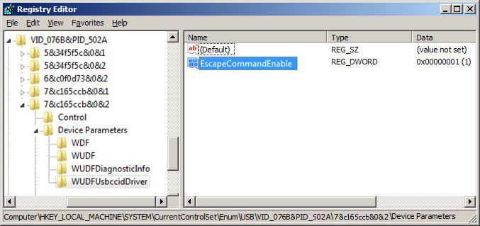
A Enabling Escape CCID commands
In order to send or receive an Escape command to a reader using Microsoft’s CCID driver, add the DWORD
registry value EscapeCommandEnable and set to a non-zero value under one of the following keys:
■ Windows 7 and 8:
HKEY_LOCAL_MACHINE\SYSTEM\CurrentControlSet\Enum\USB\VID_076B&PID_502A
\\Device Parameters\WUDFUsbccidDriver
■ Prior Windows:
HKEY_LOCAL_MACHINE\SYSTEM\CurrentControlSet\Enum\USB\VID_076B&PID_502A \\
Device Parameters
The vendor IOCTL for the Escape command is defined as follows:
#define IOCTL_CCID_ESCAPE SCARD_CTL_CODE(3500)
For details see: http://msdn.microsoft.com/en-us/windows/hardware/gg487509.aspx
If reader with different serial number is connected to computer the operation must be repeated.
May 2021 57You can also read