Room-temperature control and electrical readout of individual nitrogen-vacancy nuclear spins
←
→
Page content transcription
If your browser does not render page correctly, please read the page content below
ARTICLE
                  https://doi.org/10.1038/s41467-021-24494-x                 OPEN

                  Room-temperature control and electrical readout of
                  individual nitrogen-vacancy nuclear spins
                  Michal Gulka 1,2,3,9 ✉, Daniel Wirtitsch4,9, Viktor Ivády5,6, Jelle Vodnik 1,7, Jaroslav Hruby1,7,
                  Goele Magchiels1, Emilie Bourgeois1, Adam Gali5,8, Michael Trupke 4 & Milos Nesladek1,2,7 ✉
1234567890():,;

                  Nuclear spins in semiconductors are leading candidates for future quantum technologies,
                  including quantum computation, communication, and sensing. Nuclear spins in diamond are
                  particularly attractive due to their long coherence time. With the nitrogen-vacancy (NV)
                  centre, such nuclear qubits benefit from an auxiliary electronic qubit, which, at cryogenic
                  temperatures, enables probabilistic entanglement mediated optically by photonic links. Here,
                  we demonstrate a concept of a microelectronic quantum device at ambient conditions using
                  diamond as wide bandgap semiconductor. The basic quantum processor unit – a single 14N
                  nuclear spin coupled to the NV electron – is read photoelectrically and thus operates in a
                  manner compatible with nanoscale electronics. The underlying theory provides the key
                  ingredients for photoelectric quantum gate operations and readout of nuclear qubit registers.
                  This demonstration is, therefore, a step towards diamond quantum devices with a readout
                  area limited by inter-electrode distance rather than by the diffraction limit. Such scalability
                  could enable the development of electronic quantum processors based on the dipolar
                  interaction of spin-qubits placed at nanoscopic proximity.

                  1 Institute for Materials Research (IMO), Hasselt University, Diepenbeek, Belgium. 2 Faculty of Biomedical Engineering, Czech Technical University in Prague,

                  Kladno, Czechia. 3 Institute of Organic Chemistry and Biochemistry of the Czech Academy of Sciences, Prague, Czechia. 4 Faculty of Physics, University of
                  Vienna, Vienna, Austria. 5 Wigner Research Centre for Physics, Budapest, Hungary. 6 Department of Physics, Chemistry and Biology, Linkoping University,
                  Linköping, Sweden. 7 IMOMEC Division, IMEC, Diepenbeek, Belgium. 8 Department of Atomic Physics, Budapest University of Technology and Economics,
                  Budapest, Hungary. 9These authors contributed equally: Michal Gulka, Daniel Wirtitsch. ✉email: gulka.michal@gmail.com; milos.nesladek@uhasselt.be

                  NATURE COMMUNICATIONS | (2021)12:4421 | https://doi.org/10.1038/s41467-021-24494-x | www.nature.com/naturecommunications                                   1
ARTICLE                                                                 NATURE COMMUNICATIONS | https://doi.org/10.1038/s41467-021-24494-x

T
       he development of a physical platform for practical                   readout may therefore enable shot noise reduction due to sig-
       quantum computation is among the most compelling sci-                 nificantly higher electron detection rates compared to photon
       entific and technological goals of quantum technologies1.              counting32.
Although many recent achievements based on superconducting                      To advance towards nanoscale NV qubit systems, we demon-
circuits or trapped ions have been made, semiconductor spin                  strate the electrical readout of its basic element, a two-qubit
qubit systems may offer significantly wider electronic scalability            electron-nuclear spin system. Although the readout of large
and nanoscale device integration. Nuclear spins pose a viable                ensembles of nuclear spins has recently been achieved by using
alternative for quantum computation and, due to their excep-                 electrically-detected    electron-nuclear      double    resonance
tional isolation from the environment and resulting long coher-              (EDENDOR)36, the electrical readout of a single NV nuclear spin
ence times, they were employed in some of the early                          has remained elusive. In this work, we overcome this challenge
demonstrations of functional quantum algorithms2,3. Nuclear                  and achieve room-temperature photoelectric readout of the single
spins in solids can additionally act as quantum memories4–17,                intrinsic 14N nuclear spin of the NV centre, mediated by the
enhancing the sensitivity of quantum sensors and quantum                     electron spin, making use of the spin polarisation (and spin state
repeaters. The negatively charged nitrogen-vacancy (NV) centre               detection) near the excited-state level anti-crossing (ESLAC). We
in diamond is one of the most attractive solid-state qubit                   are able to detect nuclear magnetic resonance spectra and
platforms18–20, for which high fidelity single- and two-qubit NV              coherent spin rotations with high contrast, even for the long
electron and nuclear qubit gates21, as well as quantum error                 intervals between laser excitation pulses required for nuclear spin
correction protocols22, have been demonstrated. Consequently,                manipulation. We also provide evidence that the ESLAC condi-
surrounding 13C (nuclear spin-1/2) and 14N or 15N (nuclear spin              tions enable highly efficient MW-free protocols for the electrical
1 or 1/2) atoms can be engineered in the diamond lattice for this            detection of the nuclear spin, which are of interest for low-jitter
purpose, and control of up to 27 nuclear spins via single NV                 quantum gates. To describe the experimentally measured pho-
electron spin has been achieved23. In addition, it was demon-                toelectric detection rates, we develop a theoretical model using
strated that entanglement can be distributed probabilistically               the Lindblad master equation. The model provides an underlying
between two NV electron spin qubit nodes using a spin–photon                 theory for photoelectric readout techniques and includes charge
interface24,25, combining optical detection of magnetic resonance            state transitions, time-dependent spin polarisation and charge
(ODMR) with photon manipulation techniques. In this scenario,                carrier readout at the ESLAC. Future implementations of more
nuclear spins can serve as data qubits connected and read out by             complex schemes, such as the inclusion of nearby 13C nuclei, can
an electron spin of the nearby NV centre operating at low tem-               now be envisaged aiming towards scalable quantum hardware for
perature (~4 K)26. However, for the development of scalable                  quantum computation and sensing.
quantum computation in diamond the probabilistic nature of this
concept, as well as limited entanglement rates on the order of 40
Hz reached so-far27, represent a complex problem yet to be                   Results
solved.                                                                      Single NV photoelectrical detection and imaging. Throughout
   Here we demonstrate an approach for a quantum technology                  the experiments, a commercial IIa high-pressure high-tempera-
platform operating at room-temperature via electrically-read                 ture (HPHT) diamond (New Diamond Technology, 65%). However, in some practical applica-
additional benefits for spin readout since, in contrast to con-               tions, an increase in bias voltage might prove beneficial to
ventional optical detection schemes, it does not suffer from the             increase signal acquisition at the cost of SBC.
excited state saturation at high incoming photon fluxes31. In                    In order to reduce the photocurrent contribution induced by
the case of photocurrent, the saturation is instead given by the             photoionization of substitutional nitrogen (P1 centres, photo-
charge carrier recombination lifetime in diamond, which is sev-              ionization onset ~550 nm)37,38 frequently present in diamond
eral orders of magnitude longer than the excited state lifetime31.           crystals, we used a yellow-green 561 nm (2.21 eV) laser instead of
In combination with high electron collection efficiency, PDMR                 the commonly applied green excitation (532 nm). Optimal laser

2                NATURE COMMUNICATIONS | (2021)12:4421 | https://doi.org/10.1038/s41467-021-24494-x | www.nature.com/naturecommunications
NATURE COMMUNICATIONS | https://doi.org/10.1038/s41467-021-24494-x ARTICLE
a b 100 c 0.6 62
OPTICAL
(kcounts)
Total current
Objective - Laser focused on NV 0.3 50
Background current
Y (μm)
37
- Laser focused outside NV 0.0
36
Current (pA)
10 Dark current
(fA)
- Laser off 0.3 21
+ Electrodes - 0.6
-0.6
ELECTRICAL
-0.3 0.0
X (μm)
0.3 0.6
6
1
d Optical
5 Electrical
Z position (μm)
0.2
NV
SBC (%)
(total - background) 0 NV
Non-NV 60 SBC =
current total
current 40
FWHM
-5 2.7 μm bulk
selected voltage
Dark current 0.9 μm diamond
Single NV 20
Diamond 0 2 4 6 8 10 12 14 0 1
Voltage (V) Normalized signal (arb. units)
Fig. 1 Electrical detection of single NV centre. a Schematic of the PDMR chip with the single NV centre used for the measurements. A yellow-green 561
nm laser is focused between the contacts (with an inter-electrode distance of 3.5 µm) using a microscope objective in air (N.A. = 0.95). The resulting
currents are measured versus the bias voltage applied to the electrodes. We identify three types of currents: dark current—not related to the laser
illumination, non-NV photocurrent—laser-induced photocurrent not originating from the NV centre, NV photocurrent—current from the two-photon
ionization of the single NV centre. b Current–voltage characteristic curves for laser off (grey, dark current), for laser (4 mW) focused away from the single
NV centre (cyan, background current from dark current and non-NV photocurrent) and for laser (4 mW) focused on the single NV centre (red, total
current from dark current, non-NV photocurrent, and NV photocurrent). The bias voltage for the photocurrent measurements was set to 8.6 V as
determined from the maximum signal-to-background contrast (SBC) calculated from the background and total current (dark yellow). c, d Simultaneous
optical and electrical imaging of the single NV centre (laser power 6 mW). c XY map showing the size comparison of the same NV centre for the two
detection methods. d Z scan of the NV. Darker curves are the Lorentzian fits of the experimental data points, FWHM stands for full width at half maximum
calculated from the fitted data.
powers for photoelectric imaging of the single NV centre have spin into |ms⟩ = |0⟩39–41. This allows us to directly perform the
been previously identified to be between 2 and 4 mW31. To enable coherent nuclear spin control and sensitively obtain the spin state
detection of low average photocurrents imposed by the prolonged via photocurrent measurements, as the electron photoionization
pulse sequences needed for nuclear spin manipulation (discussed probability does depend on the electron-nuclear spin states. In
below), higher laser powers (4–6 mW) are applied here in order order to electrically detect nuclear hyperfine interactions, a pulsed
to increase the NV-generated photocurrent. Interestingly, even at lock-in envelope readout technique30 was employed (see ‘Meth-
these comparatively high laser powers, unlike photoluminescence, ods’ for more detail). In this detection method, readout laser
photocurrent does not saturate (see Supplementary Fig. 2 for pulses are solely applied during the high-state of the low-
saturation scans) and a higher S/N ratio is reached. However, frequency envelope duty cycle, while the pulsed microwave (MW)
further increase of laser power would lead to a reduction of the driving is performed continuously. The rising edge of the fre-
NV magnetic resonance contrast unless the laser readout pulses quency envelope is then used to trigger the lock-in amplifier. As
are made correspondingly shorter32. The selected NV centre was can be seen in Fig. 2b, PDMR clearly resolves the hyperfine
imaged by scanning the focused laser beam with simultaneous spectrum of a single nuclear spin close to the ESLAC.
electrical and optical detection to allow for a direct comparison
between the two readout methods (see Fig. 1c). Due to the two- Modelling. To provide a theoretical framework describing spin
photon nature of NV ionization, as well as the Gaussian beam and photoelectric transitions, we model the NV centre using the
shape after the focussing objective, electrical imaging has been Lindblad master equation. The model allows us to calculate the
shown to significantly improve both the spatial resolution and the resulting spin contrast and compare PMDR and ODMR readouts
imaging contrast31. Here, we observe an even more substantial at various experimental conditions. We utilize the following
improvement in resolution in all three dimensions, with a formalism to calculate the time dependence of the density matrix
threefold reduction of the axial size for electrical imaging (see
Fig. 1d). i y 1n y o
ρ_ ¼ H; ρ þ ∑ Γ k Lk ρLk L L ;ρ ; ð1Þ
_ k 2 k k
Photoelectric readout principle at ESLAC. A schematic of the
model describing the photoelectric readout principle at the where H and ρ are the Hamiltonian and the density matrix of the
excited-state level anti-crossing (ESLAC) is depicted in Fig. 2a, system and Lk are Lindblad jump operators carrying out non-
including charge transitions of the NV centre. The full photo- unitary transitions with rates Γ k . The model includes five elec-
ionization model is discussed in more detail in the section tronic states, namely the ground state, optical excited state, and
‘Modelling’. To achieve photoelectric readout of a single nuclear the singlet shelving state in the negative charge state as well as
spin using the NV centre electron spin as an ancilla, we first ground and excited states in the neutral charge state of the NV
polarise the 14N nuclear spin to the |mI⟩ = |+1⟩ state39–42. When centre. In the simulations, we use 13 Lindblad operators that
an external magnetic field of ~510 G (approaching the ESLAC) is describe the transitions between different electronic states (rates
aligned with the NV axis, optical pumping polarises the nuclear can be found in Supplementary Table 1). The spin Hamiltonian
spin into the |mI⟩ = |+1⟩ state (spin polarisation of >98%39) due includes electron, nuclear and hyperfine spin interactions in the
to the spin state mixing and simultaneously initializes the electron triplet ground and excited state of the NV−. The model is further
NATURE COMMUNICATIONS | (2021)12:4421 | https://doi.org/10.1038/s41467-021-24494-x | www.nature.com/naturecommunications 3
ARTICLE NATURE COMMUNICATIONS | https://doi.org/10.1038/s41467-021-24494-x
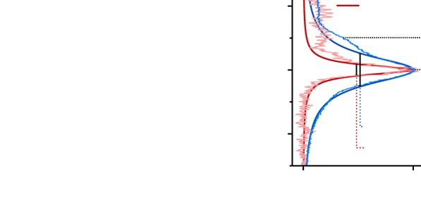
a b 2525 2530
CB e- current
0
contrast (%)
NV- NV0 1
spin mixing 2
ES 123 G
0
MS ES 1
2
contrast (%)
3
|-1>N |0>N |1>N
4
GS |-1>e
5
ESLAC ~ 510 G |-1>N |0>N |1>N
GS 6
|0>e
7
439 G
8
+
VB h current 1640 1645
MW frequency (MHz)
Fig. 2 PDMR detection at ESLAC. a Schematic describing the photoelectric readout principle at ESLAC. Only transitions responsible for the PDMR contrast
between the different electron and nuclear spin states are visualized. The |ms⟩ = |+1⟩ state, which was not probed in these experiments, is omitted for
clarity. Under the application of the magnetic field (~510 G for ESLAC), the NV− centre ground state (GS) energy levels |ms⟩ = |−1⟩ and |ms⟩ = |0⟩ are well
separated (~1.5 GHz), whereas the excited state (ES) becomes nearly degenerate resulting in spin mixing between the states with the equivalent total spin
projection quantum number. The spin mixing combined with the electron spin polarisation to |ms⟩ = |0⟩ through the metastable state (MS) [grey arrows],
results in the spin polarisation to the |ms⟩ = |0⟩ electron and |mI⟩ = |+1⟩ nuclear spin state. The yellow arrows depict optical transitions induced by the
application of the yellow-green laser. As can be seen, the |ms⟩ = |0⟩ spin sublevels in the ES are more likely to be excited by the second photon and
contribute to the photocurrent by promoting the NV electron to the diamond conduction band (CB). When this happens, the negatively charged NV−
centre is converted to NV0 centre (red arrows). The back-conversion is possible by another two-photon process while preserving the nuclear spin
orientation. First, the NV0 centre is excited to the ES and subsequently, an electron is promoted from the valence band (VB) to the vacated orbital of NV0,
leading to the formation of NV− centre. In this process the NV− |ms⟩ = |0⟩ ground states efficiently repolarise. b Pulsed PDMR measurements of the NV
nuclear (14N) and electron (ms = −1) spin hyperfine interaction for different magnetic fields showing nuclear spin polarisation close to the ESLAC
(experimental conditions for measurement at 123 G—1500 ns laser pulse of 4 mW power, 1100 ns long MW π-pulse; for measurement at 439 G—1000 ns
laser pulse of 6 mW power, 400 ns long MW π-pulse).
described in the ‘Methods’ section and is detailed in Supple- photons, charge carrier traps and recombination centres may
mentary Note 6. significantly affect electron and hole currents and their ratio. Indeed,
To determine the power-dependent ionization rates, we record nonlinear recombination processes, which may occur more sub-
time traces of the optical signal starting from different initial spin stantially at high laser powers, can enhance the PDMR contrast (see
states of the NV−. These time traces reveal important details of the Supplementary Note 7). The fundamental differences in the detection
charge state dynamics of the NV centre (see Supplementary Note 6) of ODMR and PDMR signals may provide a path to a highly efficient
and allow for validation of the model, which reproduces the PMDR quantum detection with improved contrast by optimizing
experimental PL curves (see Fig. 3a, b). In addition, it allows us to material design and device fabrication aspects.
predict the time-dependent electron and hole currents, which are not
accessible in the current experimental setup. The time dependence of
the normalized electron current closely follows the PL time traces (see Coherent electronic and nuclear qubit rotations. To coherently
Fig. 3d, e). We attribute this similarity in the dynamics of the photon drive and read out the nuclear spin at the ESLAC, we used a set of
emission and photoionization to the predominant contribution from RF pulses, applied to the nuclear spin, combined with MW-
the occupation of the NV− excited states for both processes. On the assisted electron spin readout. First, using the relatively high
other hand, we note that the amplitudes of the spin-dependent PL nuclear spin polarisation at 439 G, we probed the transition
and photocurrent signals show a different power dependence. Besides between |0,+1⟩ and |−1,0⟩ sublevels (see Fig. 4a). To include the
electrons, photo-emitted holes additionally contribute to the final radiofrequency (RF) driving necessary to manipulate the nuclear
spin contrast, prolonging it on longer timescales. Regarding the spin, the envelope lock-in readout technique30 was modified (see
power dependence of the contrast, we obtained a larger ODMR than Fig. 4b). The pulse sequence consisted of a laser pulse for spin
PDMR contrast at 1 mW and comparable ODMR and PDMR polarisation and photocurrent readout, followed by an RF pulse
contrasts at 3 mW (see Fig. 3c, f). While this trend is similar to what to drive the nuclear spin from |mI⟩ = |+1⟩ state to |mI⟩ = |0⟩
has been observed in our experiments, our microscopic model on the state and a 400 ns long MW π-pulse (MW0), set to selectively
isolated NV centre cannot quantitatively account for all the power- swap the |mI⟩ = |0⟩ electron spin from the |ms⟩ = |0⟩ state to
dependent observations. Therefore, we conclude that the residual the |ms⟩ = |−1⟩ state (see Fig. 4a). In this measurement, similarly
deviation between the experimental and theoretical ODMR and to optical detection, the nuclear spin contrast is measured
PDMR contrasts are not related to the intrinsic properties of the NV through the signal amplitudes of the particular spin states. To
centre, but rather to its lattice environment and further investigations measure the resonance frequency of the nuclear spin, an RF pulse
into the charge state dynamics are of high interest. Unlike emitted with a length corresponding to a π-rotation on the Bloch sphere
4 NATURE COMMUNICATIONS | (2021)12:4421 | https://doi.org/10.1038/s41467-021-24494-x | www.nature.com/naturecommunications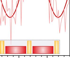
NATURE COMMUNICATIONS | https://doi.org/10.1038/s41467-021-24494-x ARTICLE
a 1 mW b 3 mW c 1 mW
Normalized PL intensity 1.1
Normalized PL intensity
1.1 ODMR
0.3
1.0 1.0 e- current
h+ current
Contrast
0.9 0.9 0.2
e- + h+ current
0.8 |0,1> 0.8 |0,1>
|0,0> |0,0> 0.1
0.7 0.7 |-1,1>
|-1,1>
|-1,0> |-1,0>
0.6 0.6 0.0
0 1 2 3 0 1 2 3 0 1 2 3
Time (μs) Time (μs) Integration time (μs)
d 1 mW e 3 mW f 3 mW
1.2 -
e current, |0,1> 1.4 -
e current, |0,1> ODMR
Normalized current
Normalized current
0.3
e- current, |-1,1> e- current, |-1,1> e- current
1.0 1.2 h+ current, |0,1>
Contrast
h+ current
0.2
h+ current, |-1,1> e- + h+ current
1.0
0.8
0.1
h+ current, |0,1>
0.8
h+ current, |-1,1>
0.6 0.0
0 1 2 3 0 1 2 3 0 1 2 3
Time (μs) Time (μs) Integration time (μs)
Fig. 3 Photon and charge carrier emission dynamics and intrinsic spin contrast. a, b The experimental (thin) and theoretical (bold) time traces of the
normalized PL intensity upon turning on the laser excitation pulse of 1 and 3 mW power, respectively, for various initial electron and nuclear spin states. For
a better visibility, the curves corresponding to |0,0⟩, |−1,1⟩ and |−1,0⟩ initial states are shifted down by 0.05, 0.1 and 0.15, respectively. To prepare different
initial spin states in the experiment, RF, MW0 and MW1 π-pulses were used (see Fig. 4a). The theoretical results closely follow the experimental curves.
d, e The time traces of the simulated electron currents (solid lines) and hole currents (dashed lines) for 1 and 3 mW laser power, respectively, for |0,1⟩ and
|−1,1⟩ initial spin states. The curves are normalized to the steady-state electron current obtained for the |0,1⟩ initial spin state. The areas below the electron
and hole currents (grey areas under the solid and dashed lines) are integrated to the same value to ensure the charge neutrality constraint of the
photoionization cycle. The difference between the solid (dashed) curves provides the spin contrast of the electron (hole) current. c, f The theoretical
ODMR contrast and the contrast of the electron-only current, the hole-only current, and the total current (PDMR) as a function of integration time for 1 and
3 mW excitation power, respectively. In the case of ODMR and PDMR, the contribution of the experimental background signal is taken into consideration
as well.
a b Envelope
|-1>e Laser
RF MW
|0>N
|1>N c d e f
0 0
|-1>N 0 0
1 1
1 1
MW0
Contrast (%)
Contrast (%)
Contrast (%)
Contrast (%)
2 2 2 2
MW1
3 3 3 3
|0>N 4 4 4 4
RF |-1,0> |-1,0> |0,0> |0,0>
5 5 τ τ 5 5 τ τ
|-1>N
|1>N π π π π π π π π
|0>e
5.00 5.05 5.10 5.15 0 50 100 5.00 5.05 5.10 5.15 0 50 100
RF frequency (MHz) RF pulse duration (μs) RF frequency (MHz) RF pulse duration (μs)
Fig. 4 Electrical readout of individual nuclear spin. a Schematic of the NV ground state hyperfine energy-level structure of the |ms⟩ = |0⟩ and |ms⟩ = |−1⟩
states depicting the resonant frequencies of the probed transitions (RF: radiofrequency, MW0: resonant microwave frequency to selectively excite the
electron spin in |mI⟩ = |0⟩, MW1: resonant microwave frequency to selectively excite the electron spin in |mI⟩ = |+1⟩). b Scheme of the envelope pulse train
designed for electrical readout of a single nuclear spin using the lock-in detection technique. Here, the lock-in amplifier is triggered by the on/off envelope
modulation of the laser pulses. c Electrically-detected RF resonant frequency of the |0,+1⟩ and |0,0⟩ transitions of the single 14N nuclear spin measured at
439 G. Inset shows the pulse sequence used, consisting of RF and MW0 π-pulses. d Corresponding electrically-detected Rabi oscillations of the single
nuclear spin with the pulse sequence shown in the inset. e Electrically-detected RF resonant frequency of the |0,+1⟩ and |0,0⟩ transitions of the single 14N
nuclear spin without electron spin manipulation measured at 439 G. Inset shows the pulse sequence used consisting of RF π-pulses. f Corresponding
electrically-detected Rabi oscillations of the single nuclear spin with the pulse sequence shown in the inset (experimental conditions: 4000 ns laser pulse
of 6 mW power, 400 ns long MW π-pulse, 1 W RF power).
NATURE COMMUNICATIONS | (2021)12:4421 | https://doi.org/10.1038/s41467-021-24494-x | www.nature.com/naturecommunications 5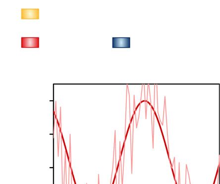
ARTICLE                                                                 NATURE COMMUNICATIONS | https://doi.org/10.1038/s41467-021-24494-x

was applied while sweeping its frequency (see Fig. 4c). The laser            spin of the NV centre. The developed theoretical model allows for
power was kept at 6 mW with a pulse duration of 4 µs where                   a precise description of spin-dependent photocurrent and its time
single nuclear spin PDMR showed a contrast close to 5%. To                   dependency at the excited-state level anti-crossing (ESLAC) and
demonstrate nuclear Rabi oscillations, the resonant RF pulse                 can be used for a highly efficient spin control and readout. PDMR
length was increased stepwise, while the distance between laser              keeps a high spin contrast, even for prolonged sequences used for
pulses was kept constant to conserve the same number of pulses               nuclear spin manipulation. The demonstration of a basic unit of a
per envelope duty cycle. The resulting electrically-detected Rabi            nuclear spin coupled to the NV electron is a first step towards the
nutation (see Fig. 4d) maintained a high contrast even for long RF           development of more complex, electrically-read gates, employing
pulse durations (up to 140 µs). We note that, depending on the               the benefits of long nuclear spin coherence in technological, solid-
duration of the nuclear spin rotation, these operations already              state electronic realizations. By providing a method for site-
correspond to an entangling CNOT gate, for which the electron                selective readout of electron spins, that further interact with
and nucleus reach their highest level of entanglement at the π/2-            adjacent nuclear spins, this work attempts to clear an important
point (~18 µs, in Fig. 4). While we do not characterize their                hurdle towards dipolarly interacted spin-qubits nodes placed in
performance here, such gates can reach high fidelity in NV                    nanoscopic proximity, and construction of diamond quantum
centres, even at room temperature43.                                         devices with semiconductor scalability. Future work is needed to
   Unlike optical detection, where a short window (typically 300             develop a site-selective individual electron spin polarisation at
ns) at the start of the readout pulse is recorded, the photocurrent          such short node distances. In this direction, the wavelength-
is integrated during the entire pulse sequence, as to date current           selective resonant spin polarisation might be used in combination
pre-amplifiers do not allow for sufficiently fast (>10 MHz) gating             with the Stark shift at low temperature45. For such control, the
with high (1012) current amplification at room temperature.                   nanoscopic electrodes used as a field gate can provide controllable
Photocurrent integration, therefore, reduces the maximum                     wavelength shift, or even manipulation with the NV charge
detected spin contrast, as both the electron and nuclear spins               state46. In addition, magnetic gradients can provide high-fidelity
are initialized within the first ~0.5 µs of the laser pulse44. Even           spin control at the nanoscale47. The rich toolbox of control
though the detected contrast decreases using longer laser pulses             methods for the NV centre therefore provides a ground for the
and higher laser powers (see Fig. 3c, f), due to intrinsic                   development of electronic diamond quantum processors and
characteristics of the readout, the PDMR contrast is maintained              scalable diamond quantum devices.
over prolonged time periods due to the hole current as devised
from the theoretical modelling above (note that the optical curves           Methods
in Fig. 3a, b are shifted for clarity). A further improvement of the         Experimental setup. The measurements were carried out using a custom-built
detected PDMR contrast is given by the slower nuclear spin                   setup allowing simultaneous optical and electrical detection (see Supplementary
polarisation of the |mI⟩ = |−1⟩ and the |mI⟩ = |0⟩ states (due to            Fig. 1a). For laser excitation, a yellow-green 561 nm gem laser from Laser Quantum
                                                                             was used with the continuous-wave power measured before the objective ranging
the spin mixing at ESLAC), which spans 3× and 2× longer                      between 4 and 6 mW. The pulses were created using acousto-optic modulator and
(respectively) than the |mI⟩ = |+1⟩ state40. Furthermore, the                the beam was focused on the sample using air objective (×40, N.A. 0.95). As-
lower technical noise, achieved using the small electrode                    purchased IIa electronic grade [111] high-pressure high-temperature diamond
architecture, and lock-in readout technique permits the high                 sample from New Diamond Technology was equipped with interdigitated contacts
nuclear PDMR spin contrast reached in our measurement.                       (3.5 µm gap) and a MW line (see Supplementary Fig. 1b, c) by means of optical
                                                                             lithography using sputtering deposition (20 nm layer of titanium covered with 100
Development of fast current preamplifiers will enable further                 nm layer of aluminium). The electrodes and the MW line were wire-bonded to the
significant improvement of the measured spin contrast.                        printed circuit board tracks. The bias electric field (~2.5 × 10⁴ V cm−1) was applied
   The scheme presented above is realised by both MW (electron)              between the electrodes and the photocurrent was collected, after preamplification
and RF (nuclear) spin driving. However, in many applications, it             (×1012, Standford Research SR570 pre-amplifier), by a lock-in amplifier (Standford
                                                                             Research SR850) referenced to the 7 Hz envelope frequency.
might be advantageous to use MW-free readout (e.g. to reduce                     Due to the fact that currently available photocurrent detection electronics do
additional heating in MW absorbing environments and/or to avoid              not offer sufficiently fast gating options for the desired electrical current
the MW resonant frequency jitter in prolonged measurements).                 amplification range, pulsed photocurrent detection is commonly averaged over the
Interestingly, the spin mixing between the nuclear and electron spins        entire pulse sequence. The comparatively long sequences required for nuclear spin
                                                                             manipulation (a factor of about 1000 compared to electron spin manipulation) can,
near the ESLAC permits to achieve such MW-free readout via the               however, result in a decreased averaged photocurrent and an excessive amount of
reverse polarisation of the electron spin by the nuclear spin40,42. To       DC noise accumulation during this period. Therefore, to circumvent this problem,
demonstrate this possibility, we modified the detection sequence              we use a low-frequency modulation that envelopes the fast laser pulses and allows
excluding the MW driving pulses. For the MW-free detection                   for frequency-filtered readout of an averaged photocurrent in a slower pulse30. This
                                                                             method, however, currently does not allow to provide time-dependent
scenario, Fig. 4e, f shows the nuclear resonances and Rabi nutations,        photocurrent detection within one laser excitation pulse. Such improvement relies
respectively. Surprisingly, we achieved a contrast similar to the MW-        on the development of fast, low-noise current preamplifiers and switches, which
assisted readout using the MW-free detection, indicating that the            would further enhance the pulsed PDMR spin contrast.
electron spin can be repolarised by the nuclear spin very efficiently,
leading to a low loss in the spin contrast. The measurements depicted        Nuclear PDMR. For nuclear spin polarisation near the ESLAC, a neodymium
in Fig. 4c–f were additionally repeated at a higher B-field of 500 G,         magnet was mounted on a holder (five degrees of freedom) and aligned to the NV
yielding similar results (see Supplementary Fig. 6), demonstrating           axis. Due to the high lateral and axial resolution of the photoelectric detection, the
that the spin mixing at ~439 G is sufficiently strong for the PDMR of         sample drift during the measurements is more prominent in the electrical signal.
                                                                             Refocusing was therefore performed between PDMR scans by maximizing the
a single nuclear spin. The differences in the spin contrast have also        pulsed photocurrent signal in all three spatial directions. For the Rabi measure-
been theoretically modelled and are further discussed in Supplemen-          ments, additional non-resonant RF (4 MHz) was applied in the sequence segment
tary Note 7.                                                                 where resonant RF and MW pulses were off, in order to provide a constant heat
                                                                             load on the sample for different resonant RF pulse durations.

Discussion                                                                   Hyperfine model and photocurrent simulations. In order to simulate the PDMR
The experimental results presented in this paper represent the               and ODMR contrast, we utilize a five-electronic-state model, see Supplementary
                                                                             Note 6. Each electronic state includes nuclear spin and electron spin degrees of
first demonstration of the photoelectrical detection of a single              freedoms. Time-dependent rates of transitions between certain electronic states are
nuclear spin at room-temperature, achieved using two-qubit spin              calculated from the population of the states, obtained from the diagonal elements
gates applied to the electron spin and the intrinsic 14N nuclear             of the time-dependent density matrix, and corresponding transition rates. Photon

6                NATURE COMMUNICATIONS | (2021)12:4421 | https://doi.org/10.1038/s41467-021-24494-x | www.nature.com/naturecommunications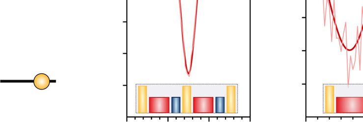
NATURE COMMUNICATIONS | https://doi.org/10.1038/s41467-021-24494-x                                                                                            ARTICLE

emission rate is determined from the calculated excited state to ground state                 18. Hanson, R., Dobrovitski, V. V., Feiguin, A. E., Gywat, O. & Awschalom, D. D.
transition rates, while charge carrier injection rate is obtained from the rate of the            Coherent dynamics of a single spin interacting with an adjustable spin bath.
photo-induced charge state transitions of the NV centre.                                          Science 320, 352–355 (2008).
   To incorporate the hyperfine interactions at the ESLAC we considered the spin               19. Nemoto, K. et al. Photonic architecture for scalable quantum information
Hamiltonians of the excited state (ES) and ground state (GS) of the negatively                    processing in diamond. Phys. Rev. X 4, 031022 (2014).
charged NV centre, which can be written as                                                    20. Doherty, M. W. et al. Towards a room-temperature spin quantum bus in
                                                                                              diamond via electron photoionization, transport, and capture. Phys. Rev. X 6,
                            2                                    2
  H ðESðGSÞ
      1Þ
            ¼ DESðGSÞ S2z     þ g e μB BSþSAESðGSÞ I þ P I 2z       g 14N μN BI; ð2Þ           041035 (2016).
                            3                                    3
                                                                                              21. Robledo, L. et al. High-fidelity projective read-out of a solid-state spin
where S and I are the electron and the 14N nuclear spin operator vectors,                         quantum register. Nature 477, 574–578 (2011).
DES ¼ 1:42 GHz is the zero-field-splitting and AES is the hyperfine tensor with                 22. Waldherr, G. et al. Quantum error correction in a solid-state hybrid spin
eigenvalues A? ¼ 27:45 MHz and Ak ¼ 41:42 MHz in the excited state, DGS and                       register. Nature 506, 204–207 (2014).
AGS are the zero-field splitting and the hyperfine tensor in the ground state48,                23. Abobeih, M. H. et al. Atomic-scale imaging of a 27-nuclear-spin cluster using
respectively, and P ¼ 5:01 MHz is the quadrupole splitting49. For the singlet                    a quantum sensor. Nature 576, 411–415 (2019).
shelving state, we used the following expression                                              24. Pfaff, W. et al. Unconditional quantum teleportation between distant solid-
                                                                                                state quantum bits. Science 345, 532–535 (2014).
                                                  2
                            H ðSS1Þ ¼ P I 2z           g 14N μN BI                   ð3Þ   25. Bernien, H. et al. Heralded entanglement between solid-state qubits separated
                                                  3
                                                                                                  by three metres. Nature 497, 86–90 (2013).
    In all electronic states, we neglected the orbital momentum degrees of freedom,           26. Bradley, C. E. et al. A ten-qubit solid-state spin register with quantum
which are indispensable for understanding the spin selective non-radiative decay                  memory up to one minute. Phys. Rev. X 9, 031045 (2019).
process but affect the spin dynamics of the electronic states negligibly16. As the            27. Humphreys, P. C. et al. Deterministic delivery of remote entanglement on a
Zeeman splitting of the doublet state NV0 suppresses hyperfine mixing between the                  quantum network. Nature 558, 268–273 (2018).
electron and nuclear spins, the electron spin degrees of freedom of the spin-1/2
                                                                                              28. Bourgeois, E. et al. Photoelectric detection of electron spin resonance of
neutral charge state can be neglected at the magnetic field values considered in our
                                                                                                  nitrogen-vacancy centres in diamond. Nat. Commun. 6, 8577 (2015).
experiments. Therefore, H ðGS  0Þ
                                   ¼ H ðES0Þ  H ðSS1Þ was used in the simulations. Due to   29. Bourgeois, E. et al. Enhanced photoelectric detection of NV magnetic
the opening of a large energy gap between the ms = +1 and other electron spin                     resonances in diamond under dual-beam excitation. Phys. Rev. B 95, 041402
sublevels in the ground and excited states of the negative charge state, only the                 (2017).
most relevant ms = {0,−1} spin states were included in our model.                             30. Gulka, M. et al. Pulsed photoelectric coherent manipulation and detection of
                                                                                                  N-V center spins in diamond. Phys. Rev. Appl. 7, 044032 (2017).
Data availability                                                                             31. Siyushev, P. et al. Photoelectrical imaging and coherent spin-state readout of
The data supporting the conclusions of this article are included within the article and in        single nitrogen-vacancy centers in diamond. Science 363, 728–731 (2019).
the Supplementary Information. In addition, the source data are available in figshare          32. Bourgeois, E., Gulka, M. & Nesladek, M. Photoelectric detection and quantum
repository with the identifier [https://doi.org/10.6084/m9.figshare.14748138.v1].                   readout of nitrogen-vacancy center spin states in diamond. Adv. Opt. Mater. 8,
                                                                                                  1902132 (2020).
                                                                                              33. Bourgeois, E. et al. in Diamond for Quantum Applications Part 2 (Elsevier,
Received: 24 February 2021; Accepted: 17 June 2021;                                               2020).
                                                                                              34. Lühmann, T., John, R., Wunderlich, R., Meijer, J. & Pezzagna, S. Coulomb-
                                                                                                  driven single defect engineering for scalable qubits and spin sensors in
                                                                                                  diamond. Nat. Commun. 10, 1–9 (2019).
                                                                                              35. Groot-Berning, K., Jacob, G., Osterkamp, C., Jelezko, F. & Schmidt-Kaler, F.
                                                                                                  Fabrication of 15NV− centers in diamond using a deterministic single ion
References                                                                                        implanter. arXiv 2101, 01979 (2021).
1.    Ladd, T. D. et al. Quantum computers. Nature 464, 45–53 (2010).                         36. Morishita, H. et al. Room temperature electrically detected nuclear spin
2.    Chuang, I. L., Vandersypen, L. M. K., Zhou, X., Leung, D. W. & Lloyd, S.                    coherence of NV centres in diamond. Sci. Rep. 10, 1–8 (2020).
      Experimental realization of a quantum algorithm. Nature 393, 143–146                    37. Rosa, J. et al. Simultaneous characterization of defect states in CVD diamond
      (1998).                                                                                     by PDS, EPR, Raman and photocurrent spectroscopies. Diam. Relat. Mater. 7,
3.    Li, Z. et al. Experimental realization of a compressed quantum simulation of a              1048–1053 (1998).
      32-spin Ising chain. Phys. Rev. Lett. 112, 220501 (2014).                               38. Heremans, F. J., Fuchs, G. D., Wang, C. F., Hanson, R. & Awschalom, D. D.
4.    Childress, L. et al. Coherent dynamics of coupled electron and nuclear spin                 Generation and transport of photoexcited electrons in single-crystal diamond.
      qubits in diamond. Science 314, 281–285 (2006).                                             Appl. Phys. Lett. 94, 152102 (2009).
5.    Neumann, P. et al. Multipartite entanglement among single spins in diamond.             39. Jacques, V. et al. Dynamic polarization of single nuclear spins by optical
      Science 320, 1326–1329 (2008).                                                              pumping of nitrogen-vacancy color centers in diamond at room temperature.
6.    Hegde, S. S., Zhang, J. & Suter, D. Efficient quantum gates for individual                   Phys. Rev. Lett. 102, 057403 (2009).
      nuclear spin qubits by indirect control. Phys. Rev. Lett. 124, 220501 (2020).           40. Steiner, M., Neumann, P., Beck, J., Jelezko, F. & Wrachtrup, J. Universal
7.    Pla, J. J. et al. High-fidelity readout and control of a nuclear spin qubit in               enhancement of the optical readout fidelity of single electron spins at
      silicon. Nature 496, 334–338 (2013).                                                        nitrogen-vacancy centers in diamond. Phys. Rev. B - Condens. Matter Mater.
8.    Asaad, S. et al. Coherent electrical control of a single high-spin nucleus in               Phys. 81, 035205 (2010).
      silicon. Nature 579, 205–209 (2020).                                                    41. Fischer, R., Jarmola, A., Kehayias, P. & Budker, D. Optical polarization of
9.    Chen, Y. H., Stearn, S., Vella, S., Horsley, A. & Doherty, M. W. Optimisation               nuclear ensembles in diamond. Phys. Rev. B - Condens. Matter Mater. Phys.
      of diamond quantum processors. N. J. Phys. 22, 093068 (2020).                               87, 125207 (2013).
10.   Gurudev Dutt, M. V. et al. Quantum register based on individual electronic              42. Smeltzer, B., McIntyre, J. & Childress, L. Robust control of individual nuclear
      and nuclear spin qubits in diamond. Science 316, 1312–1316 (2007).                          spins in diamond. Phys. Rev. A - Mol. Opt. Phys. 80, 050302 (2009).
11.   Jiang, L. et al. Repetitive readout of a single electronic spin via quantum logic       43. Rong, X. et al. Experimental fault-tolerant universal quantum gates with solid-
      with nuclear spin ancillae. Science 326, 267–272 (2009).                                    state spins under ambient conditions. Nat. Commun. 6, 1–7 (2015).
12.   Maurer, P. C. et al. Room-temperature quantum bit memory exceeding one                  44. Barry, J. F. et al. Sensitivity optimization for NV-diamond magnetometry. Rev.
      second. Science 336, 1283–1286 (2012).                                                      Mod. Phys. 92, 015004 (2019).
13.   Waldherr, G. et al. High-dynamic-range magnetometry with a single nuclear               45. Tamarat, P. H. et al. Spin-flip and spin-conserving optical transitions of the
      spin in diamond. Nat. Nanotechnol. 7, 105–108 (2012).                                       nitrogen-vacancy centre in diamond. N. J. Phys. 10, 045004 (2008).
14.   Dolde, F. et al. Room-temperature entanglement between single defect spins in           46. Krecmarova, M. et al. A label-free diamond microfluidic DNA sensor based
      diamond. Nat. Phys. 9, 139–143 (2013).                                                      on active nitrogen-vacancy center charge state control. ACS Appl. Mater.
15.   Pfender, M. et al. Nonvolatile nuclear spin memory enables sensor-                          Interfaces 13, 18500–18510 (2021).
      unlimited nanoscale spectroscopy of small spin clusters. Nat. Commun. 8,                47. Zhang, H., Arai, K., Belthangady, C., Jaskula, J.-C. & Walsworth, R. L.
      1–12 (2017).                                                                                Selective addressing of solid-state spins at the nanoscale via magnetic
16.   Reiserer, A. et al. Robust quantum-network memory using decoherence-                        resonance frequency encoding. npj Quantum Inf. 3, 31 (2017).
      protected subspaces of nuclear spins. Phys. Rev. X 6, 021040 (2016).                    48. Broadway, D. A. et al. Anticrossing spin dynamics of diamond nitrogen-
17.   Abobeih, M. H. et al. One-second coherence for a single electron spin coupled               vacancy centers and all-optical low-frequency magnetometry. Phys. Rev. Appl.
      to a multi-qubit nuclear-spin environment. Nat. Commun. 9, 2552 (2018).                     6, 064001 (2016).

NATURE COMMUNICATIONS | (2021)12:4421 | https://doi.org/10.1038/s41467-021-24494-x | www.nature.com/naturecommunications                                                       7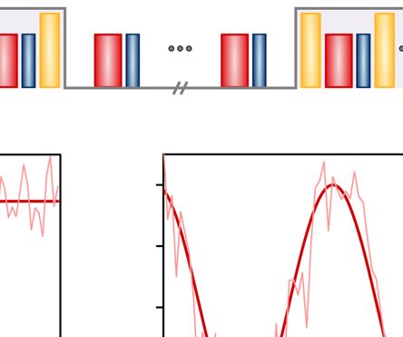
ARTICLE                                                                                  NATURE COMMUNICATIONS | https://doi.org/10.1038/s41467-021-24494-x

49. Felton, S. et al. Hyperfine interaction in the ground state of the negatively              Competing interests
    charged nitrogen vacancy center in diamond. Phys. Rev. B - Condens. Matter                The authors declare no competing interests.
    Mater. Phys. 79, 075203 (2009).
                                                                                              Additional information
                                                                                              Supplementary information The online version contains supplementary material
Acknowledgements                                                                              available at https://doi.org/10.1038/s41467-021-24494-x.
M.N. acknowledges the QuantERA projects Q-Magine and NanoSense funded through the
Flemish Scientific Foundation (FWO) as well as FWO projects G0E7417N and G0A0520N              Correspondence and requests for materials should be addressed to M.G. or M.N.
and Quantum Flagship project ASTERIQS, No. 820394. M.N. and M.G. also acknowledge the
                                                                                              Peer review information Nature Communications thanks the anonymous reviewers for
project No. GA20-28980S funded by the Grant Agency of the Czech Republic. D.W. and M.T.
                                                                                              their contribution to the peer review of this work.
acknowledge the support of the FFG through projects 864036 (QuantERA Q-Magine) and
870002 (QSense4Life). V.I. acknowledges the support from the MTA Premium Postdoctoral
                                                                                              Reprints and permission information is available at http://www.nature.com/reprints
Research Programme and the Knut and Alice Wallenberg Foundation through WBSQD2
project (Grant No. 2018.0071). A.G. acknowledges the Hungarian NKFIH grants No.
KKP129866 of the National Excellence Program of Quantum-coherent materials project and        Publisher’s note Springer Nature remains neutral with regard to jurisdictional claims in
No. NN127889 of the EU QuantERA program Q-Magine. A.G. acknowledges the support of            published maps and institutional affiliations.
the NKFIH through the National Quantum Technology Program (Grant No. 2017-1.2.1-
NKP-2017-00001) and the Quantum Information National Laboratory sponsored by Ministry
of Innovation and Technology of Hungary. The calculations were performed on resources                           Open Access This article is licensed under a Creative Commons
provided by the Swedish National Infrastructure for Computing (SNIC 2018/3-625 and SNIC                         Attribution 4.0 International License, which permits use, sharing,
2019/1-11) at the National Supercomputer Centre (NSC). J.H. is a PhD fellow of the Research   adaptation, distribution and reproduction in any medium or format, as long as you give
Foundation - Flanders (FWO).                                                                  appropriate credit to the original author(s) and the source, provide a link to the Creative
                                                                                              Commons license, and indicate if changes were made. The images or other third party
                                                                                              material in this article are included in the article’s Creative Commons license, unless
Author contributions                                                                          indicated otherwise in a credit line to the material. If material is not included in the
M.G. and D.W. conducted the measurements. V.I. and A.G. designed the theoretical              article’s Creative Commons license and your intended use is not permitted by statutory
model and V.I. carried out the simulations. M.G., E.B. and G.M. carried out experimental      regulation or exceeds the permitted use, you will need to obtain permission directly from
optimisation of detection setup. J.H., J.V. and D.W. developed acquisition software and       the copyright holder. To view a copy of this license, visit http://creativecommons.org/
tailored the setup for photocurrent readout gates. M.N., M.T. and A.G. supervised partial     licenses/by/4.0/.
sub-projects and took part in detailed discussions of results. M.G., D.W., V.I., A.G., M.T.
and M.N. contributed to the manuscript writing. All authors discussed the results and
                                                                                              © The Author(s) 2021
commented on the manuscript. M.N. supervised the joint efforts.

8                      NATURE COMMUNICATIONS | (2021)12:4421 | https://doi.org/10.1038/s41467-021-24494-x | www.nature.com/naturecommunications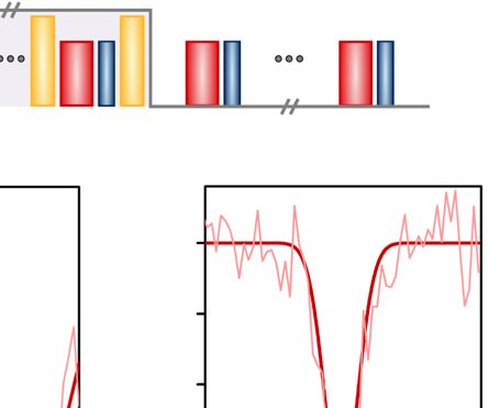
You can also read


