Siltronic - Well positioned for the future - Dr. Christoph von Plotho, CEO May 28, 2019 - Siltronic AG
←
→
Page content transcription
If your browser does not render page correctly, please read the page content below
Siltronic – Well positioned for the future

Dr. Christoph von Plotho, CEO
May 28, 2019

                                             © Siltronic AG
Overview
Semi applications Semiconductor end markets growth fuelled by innovation such as Big
Data, 5G connectivity, electrification, energy reduction and Artificial
Intelligence
Moore’s Law continues but slowing down
Industry innovation Continued process technology innovation attracts new applications
and increases wafer volume
Customer roadmaps require wafers to accommodate latest Design
Rules and new specifications
Stakeholder value We continue to execute our strategy to stay “one generation ahead”
Grow with the market and deliver value to our stakeholders
Siltronic AG – Capital Markets Day Siltronic – Well positioned for the future
May 28, 2019
2 of 28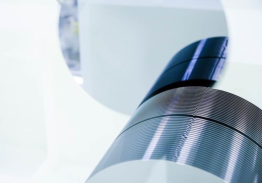
SEMI END MARKETS

                   © Siltronic AG
Data creation and increasing storage demand will grow further
Smartphones PCs/Laptops Servers
Forecasted to remain rather Increasing SSD ratio and SSD
Increasing content in flattish in silicon demand size
smartphones
more cameras per phone upside potential with Substitution of HDD by SDD due
including 3D sensing increasing SSD ratio to performance
memory (DRAM + NAND) Main server applications:
software as a service (SaaS)
machine learning
Pictures: zapp2photo/stock.adope.com, Denis Rozhnovsky/stock.adobe.com, phonlamaiphoto/stock.adobe.com
Siltronic AG – Capital Markets Day Siltronic – Well positioned for the future
May 28, 2019
4 of 28
Automotive and industrial applications offer multiple growth
opportunities
Automotive Industrial
Powerertrain, Chassis, Infotainment and ADAS drive Industrial semiconductor devices highly fragmented
Si consumption Main device groups are sensors, analog, logic and
Si consumption for powertrain influenced by hybrid power
solutions and electrical cars Industrial devices follow the main function chain of
Chassis Si consumption driven by a multitude of sense - convert signal - transfer signal – process –
small devices for mechanical, electrical and sensing save – and control power of the device.
actions in and around the car
ADAS, Infotainment and connectivity require Si content growth driven by cost reduction initiatives:
sensors, advanced Logic and larger areas of inverters, predictive maintenance and cobots and less
memory by end market volumes.
Pictures: ekkasit919/stock.adobe.com, denisismagilov/stock.adobe.com
Siltronic AG – Capital Markets Day Siltronic – Well positioned for the future
May 28, 2019
5 of 28
Main end applications drive different wafer sizes

Si consumption share per main end market, in % of total wafer area in 2018

                     20
                                                                              32
                                                                                                                         45

                     34
                                                                              19
                                                                                                                          4
                                                                               5                                          4
                                                                               1
                     21                                                                                                  27
                                                                              25

                     14
                      5                                                       18                                         20
                      6
                 300 mm                                                  200 mm                                          SD
                          Automotive            Industrial         SSD             PC/Servers             Smartphone   Other

           Siltronic AG – Capital Markets Day                Siltronic – Well positioned for the future
           May 28, 2019
                                                                                                                               6 of 28
INDUSTRY INNOVATION

                      © Siltronic AG
Diversified markets driving differentiation for silicon wafers must
be fitted to varied device approaches

Complexity increases over time
                                                                                       Nanotubes,                 New Materials
Complexity                                                                             Nanosheets,
                                                                                       Cobalt
                                                Alternative materials                                             Complex Device Structures
                                                in Power:
                                                GaN, SiGe, SiC
                                                                                                                  Continued DR Shrink
                                                            3D Structures
                                                            and stacking                     7nm

        Lower Resistivity                                                       10nm                              Packaging Advances
                                         FinFet
                                                               14nm

                                                    20nm                               3D Packaging

                                    28nm                          2.5 Packaging
 Planar CMOS
                       32nm

             45nm                       System on Chip

 65nm
                                                                                                           Time
                                                                                                                                  Sources: Siltronic Marketing

               Siltronic AG – Capital Markets Day             Siltronic – Well positioned for the future
               May 28, 2019
                                                                                                                                                    8 of 28
Siltronic is continuously improving its wafer properties to match
customer needs
Higher integration Lower power Flatter wafers Tailored resistivity
consumption specifications
Faster circuits Lower defect density
Higher temperature Enhanced carrier
Smaller transistors Fewer particles at lifetime
Higher power smaller size
Line width reduction Advanced materials
Higher die yield Less edge exclusion
Picture: Szasz-Fabian Jozsef/stock.adobe.com
Siltronic AG – Capital Markets Day Siltronic – Well positioned for the future 9
May 28, 2019
9 of 28
Wafer technology requires perfection in all aspects
Example: 300 mm wafer
Clean air production
For clean room class 1, 3 m
length, >400 kg weight)
Purity of silicon wafers
Case study: yield enhancement in customer device line
Objective Siltronic contribution Customer contribution
Improve device performance Providing a sample wafer Device process runs
related to an electrical test set with ingot
parameter (leakage current) characteristics. Physical Feedback of
wafer characterization and electrical
Define range / limits of specific heat treatments to test parameters
dopants impurities to better condition dopants /
understand the failure impurities of test wafers
mechanism
Result Optimized specification for certain ingot and wafer characteristics,
resulting in stable and reliable yields and device performances
Picture: Damir Fajic /stock.adobe.com
Siltronic AG – Capital Markets Day Siltronic – Well positioned for the future 11 11 of 28
May 28, 2019Case study: future design rule generation material and processes
Objective Siltronic contribution Customer contribution
Integrate silicon wafers with Hetero-epitaxial sample Device process tests
non silicon channel material wafers with various SiGe and feedback on
to achieve sub 10nm DR layer compositions, with or sample wafer
generation transistors without strained silicon or performance, device
Explore silicon wafer germanium layers. Material characterization data
options based on Siltronic characterization data and assessment of
available products and applicability of different
processes options
Early identification of potential options
Result
Positioning of Siltronic as development partner of choice
Picture: Vasily Smirnov /stock.adobe.com
Siltronic AG – Capital Markets Day Siltronic – Well positioned for the future 12 12 of 28
May 28, 2019Case study: wafer and defect characterization equipment
development
Objective Siltronic contribution Customer contribution
Define and standardize Measurements with various Same as Siltronic
measurement recipes to settings, measurement
balance the need for capability analysis and
sensitivity and cost proposals for best known
optimization to enable method
device process
development
Aligned / correlated measurement recipes for newest
Result generation of measurement equipment
Ability to verify product performance against customer
expectation at acceptable cost per wafer
Picture: Alphonse Mc Clouds /stock.adobe.com
Siltronic AG – Capital Markets Day Siltronic – Well positioned for the future 13 13 of 28
May 28, 2019Czochralski (CZ) vs Floatzone (FZ) crystal growing process
Czochralski (CZ)-growth
Whole silicon charge molten at a time
Dopant enriches during ingot pulling in the crucible with
decreasing amount of molten silicon left in the crucible
Resistivity drops towards ingot tail end
FZ-growth
Only a relatively small amount of silicon molten at a time
Dopant is added as a gas blown towards the molten zone
Hardly any axial effect
Siltronic AG – Capital Markets Day Siltronic – Well positioned for the future
May 28, 2019
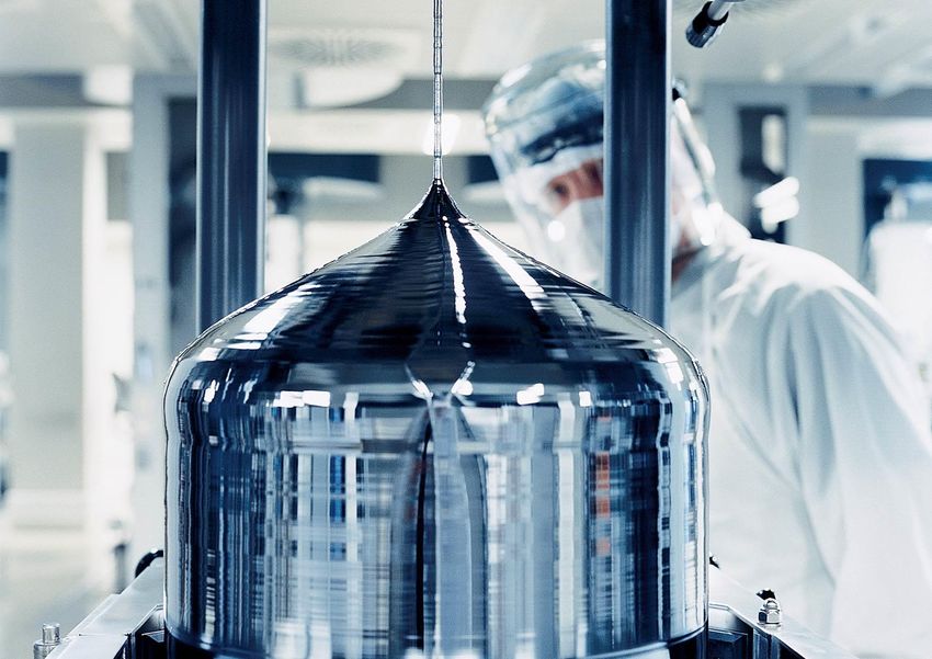
14 of 28Epitaxial wafers provide perfect solution for leading edge device
technologies
Homoepitaxy: „substrate layer = epi layer Epi process step
Si Epi
Si Substrate
Epitaxial layer provides Target applications
Defect free surface and subsurface layer Logic
Excellent gate oxide quality CMOS image sensors
Tighter resistivity distribution than polished wafers
No slip issues
Siltronic AG – Capital Markets Day Siltronic – Well positioned for the future
May 28, 2019
15 of 28Floatzone (FZ) technology
FZ development history FZ crystal growing
200 mm
150 mm
1"
1955 1990 2005
Properties of FZ Target applications
Excellent resistivity uniformity IGBT & Diode
Optimized purity of bulk material Replacement for thick epi
Significantly lower oxygen content High ohmic applications (passive integration, RF)
High resistivity
Siltronic AG – Capital Markets Day Siltronic – Well positioned for the future
May 28, 2019
16 of 28R&D activities on GaN-on-Si for emerging niche markets
Structure of GaN-on-Si
GaN active
device layer
Buffer layer
Nucleation layer
Silicon substrate 8“ GaN-on-Si wafer Microscopic inspection
General benefits Target applications
Fast switching Power electronics
Reduction of conduction and switching losses Low/high voltage and high frequency applications, e.g.
High temperature operation Power supplies for consumer electronics
Power converters for solar
Compatible with Si CMOS manufacturing Devices for automotive
RF electronics
5G telecom infrastructure, mm wave front-end
Siltronic AG – Capital Markets Day Siltronic – Well positioned for the future
May 28, 2019
17 of 28STAKEHOLDER VALUE
© Siltronic AGSiltronic has a relevant global market share…
Top 5 wafer producers serve more than 90% of market across all diameters
17% 11%
15%
27%
30%
SK Siltron Siltronic Shin Etsu Sumco GlobalWafers
Sources: reported company revenues FY 2018, converted to USD million
Siltronic AG – Capital Markets Day Siltronic – Well positioned for the future
May 28, 2019
19 of 28... and an international manufacturing network
Freiberg CP* 300 mm
Germany
Portland 200 mm
United States
Burghausen CP* 300 mm SD*
► Central R&D hub in Burghausen
► High volume facilities for 300 mm
in Germany and Singapore
► Among world’s newest & largest SSW CP* 300 mm SSP 200 mm
fabs in Singapore
Singapore
*CP = Crystal Pulling | *SD = 150 mm and smaller
Siltronic AG – Capital Markets Day Siltronic – Well positioned for the future
May 28, 2019
20 of 28Clear commitment to sustainability
Sustainability at Siltronic AG
Claim: We understand sustainability as responsible action for society and
want to generate competitive advantages through sustainable action.
Strategy: We plan resource-saving right from the start, based on product and
production safety as well as health and environmental protection.
Voluntary commitments: We follow the principles of the Sustainable
Development Goals, the United Nations Global Compact, and the Responsible
Care and Responsible Business Alliance initiative.
Goal: We want to reconcile the effects of our business activities with the
expectations and needs of society.
Investor-Rating: Since 2018, we have been analyzed by ISS-oekom, one of the
world's leading rating agencies for sustainable investments, and assessed with
regard to the ESG criteria (Environment, Social, Governance). Right from the start,
we were awarded ‘Prime’ status for our sustainability activities.
Siltronic AG – Capital Markets Day Siltronic – Well positioned for the future
May 28, 2019
21 of 28Environment - Efficiency as a success factor
Selection of non-financial performance indicators in 2018
Raw Material Energy
Energy consumption
Silicon yield per wafer area
improved by decreased by
1% 3%
vs. 2017 vs. 2017
Recycling Occupational Safety
The share of returnable The number of accidents
packaging per wafer at work per 1 million
area was hours worked was
32 % 1.9
Siltronic AG – Capital Markets Day Siltronic – Well positioned for the future
May 28, 2019
22 of 28History of technology innovation and cost optimization ideally
positions Siltronic for future success
Strong position
for the future
Technology milestones
First 200 mm wafer produced
First 300 mm R&D project
First 300 mm pilot plant
First 300 mm production in Freiberg
First 300 mm wafer out of SSW
Development node 7/8 initiated
DR 11 commercialized
Development node 5 initiated
node 7/8 commercialized
Development node 3
initiated
2015 2016 2017 2018 2019
1968 1978 1984 1990 1995 1997 1998 2000 2004 2006 2008 2012 2014
Groundbreaking new
crystal pulling hall in
Inauguration
Singapore
Corporate milestones
new crystal
IPO pulling hall in Freiberg
Increase stake in SSW to 78%
Closure of Hikari facility
50:50 JV with Samsung for 300mm facility (“SSW”)
100% stake in NSC Electron Corporation in Hikari (Japan)
Foundation of Wacker Siltronic Singapore Pte. Ltd (“SSP”)
Acquisition of Freiberg facility
Foundation of Wacker Siltronic Corporation in Portland (US)
Foundation of Wacker-Chemitronic GmbH
Source: Company information
Siltronic AG – Capital Markets Day Siltronic – Well positioned for the future
May 28, 2019
23 of 28Siltronic strategy - capitalize on market opportunities while focusing
on 300 mm & technological leadership
Optimize returns,
stay ahead in technology and
grow with the market
Strategic Focus
Grow Ensure Improve Execute
with the market technology & financial performance cost reduction
quality leadership & cash flow roadmaps &
debottlenecking
concepts
We continuously increase the value for our stakeholders by providing best-in-class wafers
at competitive costs.
Siltronic AG – Capital Markets Day Siltronic – Well positioned for the future
May 28, 2019
24 of 28Investment Highlights – Siltronic Strengths
Market position Strong market position in the semiconductor and wafer industry
Strategy Technology and quality leadership
Customers Supplier to all top 20 silicon wafer consumers
Financials Profitability increase and on-going efficiency improvement
Products High-quality wafers made of hyperpure silicon
Management Experienced management team and highly skilled workforce
Siltronic AG – Capital Markets Day Siltronic – Well positioned for the future
May 28, 2019
25 of 28Contact and Additional Information
Issuer and Contact Additional Information
Siltronic AG ISIN: DE000WAF3001
Hanns-Seidel-Platz 4 WKN: WAF300
D-81737 München Deutsche Börse: WAF
Listing: Frankfurt Stock Exchange
Investor Relations:
Prime Standard
Petra Mueller
email: petra.mueller@siltronic.com
Tel. +49 89 8564-3133
Financial Calendar
Half Year Report July 25, 2019
Q3 Quarterly Statement October 24, 2019
Siltronic AG – Capital Markets Day Siltronic – Well positioned for the future
May 28, 2019
26 of 28Disclaimer
The information contained in this presentation is for background purposes only and is subject to
amendment, revision and updating. Certain statements contained in this presentation may be
statements of future expectations, future financial performance and other forward-looking statements
that are based on management's current views and assumptions and involve known and unknown risks
and uncertainties. In addition to statements which are forward-looking by reason of context, including
without limitation, statements referring to risk limitations, operational profitability, financial strength,
performance targets, profitable growth opportunities and risk adequate pricing, words such as "may”,
“will”, “should”, “expects”, “plans”, “intends”, “anticipates”, “believes”, “estimates”, “predicts”, “continue”,
“projects” or “seeks”, “potential”, “future”, or “further” and similar expressions may identify forward-
looking statements. By their nature, forward-looking statements involve a number of risks, uncertainties
and assumptions which could cause actual results or events to differ materially from those expressed or
implied by the forward-looking statements. These include, among other factors, changing business or
other market conditions, currency and interest fluctuations, introduction of competitive products, poor
acceptance of new products and services, change of the corporate strategy and the prospects for
growth anticipated by the management. These and other factors could adversely affect the outcome and
financial effects of the plans and events described herein. Statements contained in this presentation
regarding past trends or activities should not be taken as a representation that such trends or activities
will continue in the future. Siltronic AG does not undertake and does not intent to undertake any
obligation to update or revise any statements contained in this presentation, whether as a result of new
information, future events or otherwise. In particular, you should not place any reliance on forward-
looking statements which speak only as of the date of this presentation.
Siltronic AG – Capital Markets Day Siltronic – Well positioned for the future
May 28, 2019
27 of 28SILTRONIC AG | Hanns-Seidel-Platz 4
81737 Munich
Germany
© Siltronic AGYou can also read