Simulations of radiation hard detectors for timing applications - CERN Indico
←
→
Page content transcription
If your browser does not render page correctly, please read the page content below
Simulations of radiation hard
detectors for timing applications
F. Moscatelli(1,2), D. Passeri(3,2), A. Morozzi(2), T. Croci(3,2),
 P. Asenov(1,2), M. Menichelli (2), G.M. Bilei(2)
 (1) IOM-CNR Perugia, Perugia, Italy
 (2) INFN Perugia, Perugia, Italy
 (3) DI, University of Perugia, Perugia, Italy
AIDAinnova - Motivations
✓ INFN and University of Perugia are involved in WP6 Task 6.2
• Simulations of surface and bulk radiation damage for 4D (tracking+timing) detectors
 toward more radiation tolerant solutions
Calibration/extension of the previously developed simulation models
 Calibration/extension of the previously developed models (“Perugia model” and its recent upgrade) by
 comparing the simulation findings with measurements carried out on dedicated test structures as
 well as on different classes of 3D and LGAD detectors.
Study the effect of surface and bulk radiation damage with reference to 4D (tracking+timing)
detectors toward more radiation resistance solutions.
 The proposed activity will focus specifically on disentangling the effects of the two main radiation
 damage mechanisms, e.g. the surface damage due to ionizing effect and the bulk damage due to
 atomic displacement, with reference to 4D detectors toward more radiation resistance solutions.

 2/16
 AIDAinnova , kick-off meeting, April 2021
LGAD simulations

 In collaboration with
 INFN Torino
 Calibration/extension
 of the previously
 developed models by
 comparing the
 simulation findings
 with measurements
 carried out on
 different classes of
 LGAD detectors

 In the framework of the PRIN 4DInSiDe project

 AIDAinnova , kick-off meeting, April 2021 3/16
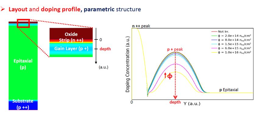
TCAD simulation of LGAD devices
✓ Physical models ✓ Radiation damage models
✓ Generation/Recombination rate ✓ “New University of Perugia model”
 • Shockley-Read-Hall (SRH), Band-To-Band • Combined surface and bulk
 Tunneling (BTBT), Auger TCAD damage modelling scheme[3]
 • Avalanche Generation • Traps generation mechanism
 => impact ionization models, such as ✓ Acceptor removal mechanism
 van Overstraeten-de Man, Okuto-Crowell,
 Massey[2], UniBo
✓ Carriers mobility variation doping and field
 dependent where
✓ Physical parameters • Gain Layer (GL)
 • e-/h+ recombination lifetime • c, removal rate, evaluated using the
 • surface recombination velocity Torino parameterization[4]

[2] M. Mandurrino et al., Numerical Simulation of Charge Multiplication in
Ultra-Fast Silicon Detectors (UFSD) and Comparison with Experimental
 [3] AIDA2020 report, TCAD radiation damage model - CERN Document
Data, IEEE, 2017
 Server
 [4] see M. Ferrero talk, Tredi workshop 2021

 AIDAinnova , kick-off meeting, April 2021 4/16
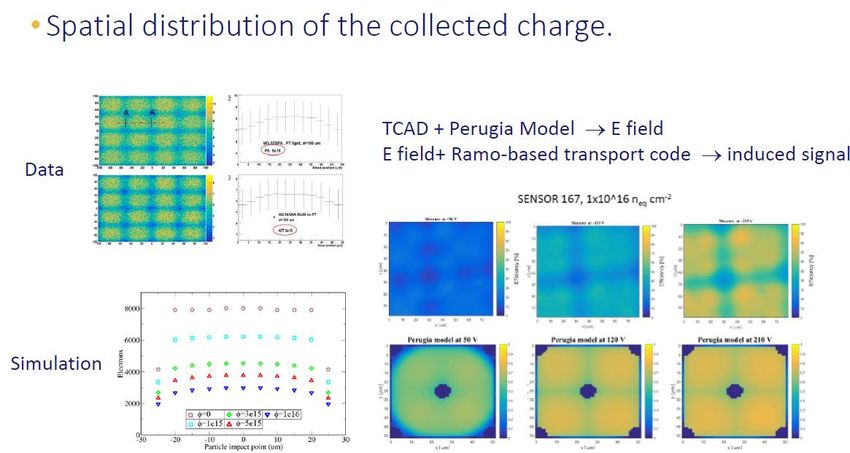
Methodology
 DC / AC analysis Transient analysis Gain calculation
 •DC biasing (static) •For each DC bias step, one •Leakage current calculation
 o n cathode: 0 V Time-Variant (TV) simulation of o instant = 0,9 ns
 o p anode: sweep impinging particle (MIP),
 ✓ start = 0 V •Leakage current offset subtracted
 ✓ step = - 25 V (from 100 V)
 following the “HeavyIon” model from the simulated I(t) curve
 ✓ stop = - 1000 V o instant of penetration, 1ns
 o impinging point, 10 µm •Calculation of Collected Charge
 •AC biasing (small-signal) o through the whole device (CC) as the integral of the current
 o For each DC bias step, o Linear Energy Transfer (LET)
 superimposition of a
 = = [6]
 1 Vpp, 1 kHz sinusoid µ
 o Impedance matrix for each where
 node of the discretized grid = 3,68
 [5]
 ELOSS = 0,027 + 0,126 µ

 [5] S. Meroli et al., Energy loss measurement for charged particles in very thin silicon layers, JINST 6 P06013, 2011
 [6] V. Sola et al., First FBK production of 50 µm ultra-fast silicon detectors, Nucl. Instrum. Methods Phys. Res. A, 2019

 AIDAinnova , kick-off meeting, April 2021 5/16
Analysis of different avalanche models
✓ Simulation results, before irradiation
 Good agreement
 I-V with experimental
 Temperature 300 K
 Electrical contact area
 data
 1mm2 for Massey model
 Cut of the electric field for different Vbias

 ZOOM
 [6]

[6] V. Sola et al., First FBK production of 50 µm ultra-fast silicon detectors, Nucl. Instrum. Methods Phys. Res. A, 2019

 AIDAinnova , kick-off meeting, April 2021 6/16
Static (DC) and small-signal (AC) behavior (1/5) ✓ Simulation results, before and after irradiation I-V C-V 1e-2 φ 1e-4 φ φ φ 0 Massey model. Temperature 300 K. Electrical contact area 1mm2 AIDAinnova , kick-off meeting, April 2021 7/16
Static (DC) and small-signal (AC) behavior (2/5)
✓ Comparison with experimental data, before irradiation Good
 agreement!
 I-V C-V

 Massey model. Temperature 300 K. Electrical contact area 1mm2

 AIDAinnova , kick-off meeting, April 2021 8/16
Static (DC) and small-signal (AC) behavior (3/5)
✓ Comparison with experimental data, fluence 2.0e14 neq/cm2 Good
 agreement!
 I-V C-V

 1e-2

 1e-4

 Massey model. Temperature 300 K. Electrical contact area 1mm2

 AIDAinnova , kick-off meeting, April 2021 9/16
Static (DC) and small-signal (AC) behavior (4/5)
✓ Comparison with experimental data, fluence 8.0e14 neq/cm2 Good
 agreement!
 I-V C-V

 1e-2

 1e-4

 Massey model. Temperature 300 K. Electrical contact area 1mm2

 AIDAinnova , kick-off meeting, April 2021 10/16
Static (DC) and small-signal (AC) behavior (5/5)
✓ Comparison with experimental data, fluence 1.5e15 neq/cm2 Good
 agreement!
 I-V C-V

 1e-2

 1e-4

 Massey model. Temperature 300 K. Electrical contact area 1mm2

 AIDAinnova , kick-off meeting, April 2021 11/16
Transient response in progress ✓ Comparison between LGAD and PIN response to the MIP for different Vbias I-t, before irradiation I-t, fluence 1.5e15 neq/cm2 ZOOM ZOOM φ __ LGAD (y-axes left side) …. PIN (y-axes right side) Massey model. Temperature 300 K. Electrical contact area 1mm2 AIDAinnova , kick-off meeting, April 2021 12/16
Work plan: simulations
 ✓ Bulk radiation damage modelling for 3D and LGAD :
 • Extension of the three-level UniPG modelling for 3D
 • Understanding of dopant deactivation effects for LGAD within the
 radiation damage model – electrical analysis of the intentional
 introduction of impurities [e.g. Carbon] with specific test structures, e.g.
 Van der Pauw structures.
 • Model validations via comparison with available test measurements.
 • Identification of the most radiation-hard structures for both devices.

 Refinement of the Surface radiation damage modelling:
 - Comparison with literature data/dedicated measurements in terms
 of static parameters (R, C) and charge collection properties.
 ✓ Comprehensive modelling (bulk + interface, 2D/3D).

 AIDAinnova , kick-off meeting, April 2021 13/16
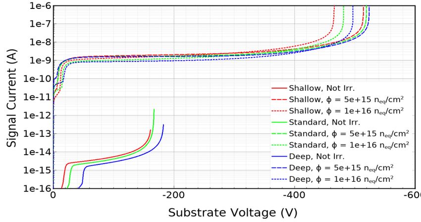
Application of the developed model Doping profiles Shallo ✓ Thin wafers recently produced by FBK w • thickness 25 and 35 µm [7] Standar d ✓ TCAD simulations very useful to Deep • compare the results with the experimental data, before and after I-V φ irradiation (irradiation campaign just completed at the Ljubljana JSI facility up to 1.0e17 neq/cm2) • designing the future productions of φ thin LGADs for extreme fluences 0 [7] V. Sola et al., First results from thin silicon sensors for extreme fluences, 37th RD50 Workshop, Zagreb, Croatia, 2020 Massey model, Temperature 300 K. AIDAinnova , kick-off meeting, April 2021 14/16
Collaboration with Trento for 3D
 Collaboration
 with Trento to
 extend the
 bulk+surface
 model to
 reproduce the
 macroscopic
 behaviour of
 3D detectors

 AIDAinnova , kick-off meeting, April 2021 15/16
Conclusions
✓ Strategy for the numerical simulation of LGAD devices.
✓ First Results obtained under different operative conditions (device biasing, fluence).
✓ Good agreement between simulation predictions and experimental data for both non-irradiated
 and irradiated LGAD device.
✓ Extension of “new University of Perugia TCAD model” in order to simulate the radiation
 damage effects on 3D and LGAD detectors

✓ Application of the validated simulation framework for the prediction of different design
 options/detector geometries (e.g. thin sensors) behavior

 AIDAinnova , kick-off meeting, April 2021 16/16
You can also read