Testing Results for a Video Poker System on a Chip
←
→
Page content transcription
If your browser does not render page correctly, please read the page content below
Testing Results for a Video Poker System
                on a Chip
                          Preston Thomson and Travis Johnson

Introduction-
This report examines the results of a system on a chip SoC video poker system. The
report will begin with a short description of the project. It will then exam the testing
methods employed. The results of the project will be shown pictorially and discussed.
Finally, the paper will conclude with the authors’ opinions of the project including
changes to the design that could be made in future design iterations and what the authors
learned over the course of study.
This SoC video poker system is a basic implementation of a slot machine. Essentially the
project can be broken into two main modules: the VGA display controller and the poker
engine. The VGA controller is responsible for displaying the game board, the five cards
that make up the current hand (the cards toggle color based on their held status) and the
bank displayed in hexadecimal (because binary is boring, just like synchronous design).
The VGA controller accepts data from the poker engine. It is based on a 25 MHz clock
for compatibility with standard VGA monitors. The display is a fairly standard 640x480
pixel resolution. The system outputs are meant to be wired to a standard 15 pin VGA
connector. The output is RGB standard with vsync and hsync values set to the VGA
standard.
The poker engine is the guts of the system. It takes inputs from several switches. There
are two resets, a deal/draw button and 5 inputs to hold or release each respective card.
The system generates 5 random cards that are checked for validity through a hardware
redundancy checking module. Each individual card is generated through a series of
LFSRs. Once 5 random cards are generated into a valid hand, the player has the option to
mark cards to hold and then finish the hand by pushing draw. The hand is then sorted
internally with a bubble sort and checked for wins versus known combinations. In the
case of a win, the bank is then incremented. At this point, the game is ready for the next
hand. The system was designed in Verilog HDL, synthesized with synopsys tools using
the UofUdigital library and simulated with the Cadence Design Suite. More information
on this project including specific Verilog details is available in the authors’ final report
on this project from ECE6710.
The project was attached to a University of Utah pad ring. The chip area including the
pads was 4 TCUs. The design was submitted for fabrication in the .5 micron 3 metal, 2
poly process using AMI design rules. The fabrication was performed by MOSIS, and the
finished design is housed in an 84-pin ceramic PGA. The remainder of this report will
cover the test setups and results.

Testing Methodology-
Initial functional testing was performed on the original verilog code using a Xilinx
Spartan II FPGA. This design was synthesized using Xilinx ISE to produce a bitfile that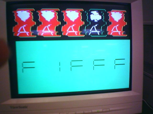
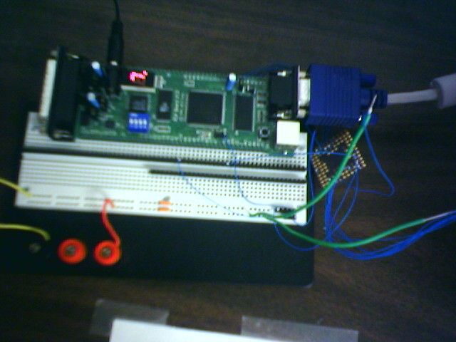
was subsequently tested by loading the file onto a Spartan II based XESS XSA board.
This board had plenty of inputs, a VGA output and an adjustable oscillator.
The board was then connected to a VGA monitor and the game was put to a priori tests.
There were a few errors discovered through these first tests. There were some interesting
errors with duplicate cards and a few graphical glitches. The design was then retested
against verilog test benches (all these files are available with in the 6710 report and will
soon be posted on Travis Johnson’s website) and the state machine design was slightly
altered to correct the errors.
Once these errors were corrected the design was resynthesized and loaded back to the
board. After extensive physical testing the board was deemed error free. The verilog code
was then resynthesized with the synopsys design compiler and other tools such as silicon
ensemble and Layout XL to generate the layout. The layout was DRCed and LVSed in
Virtuoso then fitted to the University of Utah Pad ring. A small scale testing was
performed, but due to time and resource constraints (lab quotas) only about 12 ms of code
could be tested against the circuit. More testing information can be found in the previous
paper detailing the design of this work.
Once the fabricated chips were returned the chips were put to physical testing. Since the
project was based on video, the bulk of testing was completed by wiring the chip up and
verifying its functionality by trying to play the game. Initially, the chips were to be
soldiered onto PCBs designed by one of the authors, but the boards were not ready in
time for the testing. Instead, the chip was wired up to the XESS board and tested using its
switches and clock as pictured below in figure 1.
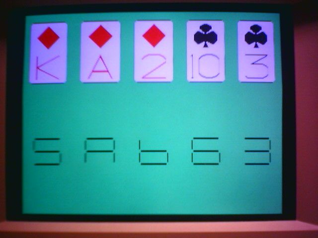
Figure 1: Chip connected to the XESS XSA board.

Unfortunately, the internal clock had a very low voltage (about 1.5v peak to peak). To
compensate, a simple verilog code (out
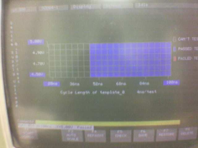
Figure 3: Chip and 25 MHz oscillator

All though the display worked correctly, there were other problems. The system was
supposed to go into a default state of a hand showing all 2’s of diamonds, but instead it
displays all aces. The bank also didn’t start at the proper value of 64h, instead it is always
a random value. The resets on the board seem to work, but the game does not function
when pushing the deal/draw button. The authors believe that the different synthesis tools
may have changed the design during optimization. The chip was examined under a
microscope to ensure that the general layout had been retained. No errors were found.
The fact that the VGA controller also functions leads to the conclusion that the error is of
a logic synthesis level and not a fabrication issue.

                   Figure 4: Valid Hand Shown With Proper Oscillator
Schmoo-
The chips were also put through a brief schmoo test against voltage and cycle time. The
results are shown below along with the msa file. It passed in all cases.
Figure 5: Schmoo Plot
Conclusions-
Overall, the project was very interesting to test. The authors learned the importance of
adding more test structures like a ring oscillator at the least. The schmoo plot passed
every test. This may be an indication that there may have been a problem with the choice
of schmoo parameters for vsync and hsync. If the project were to be redone, the authors
would definitely add more testing structures and integrate an oscillator that could be used
to clock the circuit. It would also be nice to have the computing resources to carry out a
longer test run and simulate more hands post synthesis. It also would have been nice to
get the chips on a PCB for more direct reliable access than what was possible through
wire wrapping to an XSA board.You can also read