The scientific payload on-board the HERMES-TP and HERMES-SP CubeSat missions - arXiv
←
→
Page content transcription
If your browser does not render page correctly, please read the page content below
The scientific payload on-board the HERMES-TP and HERMES-SP
                               CubeSat missions

Y. Evangelista*a,b, F. Fiorec, F. Fuschinod,e, R. Campanad,e, F. Ceraudoa, E. Demenevf, A. Guzmang,
     C. Labantid, G. La Rosah, M. Fiorinii, M. Gandolaj, M. Grassik, F. Melej, D. Milánkovichl,
 G. Morganted, P. Nogarah, A. Pálm, R. Piazzollaa, S. Pliego Caballerog, I. Rashevskayan, F. Russoh,
 G. Sciarronea, G. Sottileh, F. Ambrosinoa, N. Auricchiod, M. Barberao,p, P. Belluttif, G. Bertuccioj,
 G. Borghif, J. Caoq, T. Chenq, G. Dilillor, M. Ferocia,b, F. Ficorellaf, U. Lo Ciceroo,p, P. Malcovatik,
  A. Morbidinia, G. Paulettar, A. Picciottof, A. Rachevskis, A. Santangelog, C. Tenzerg, A. Vacchir,
   L. Wangq, Y. Xuq, G. Zampas, N. Zampar,t, N. Zorzif, L. Burderiu, M. Lavagnav, R. Bertacinw,
        P. Lunghiv, A. Mongex, B. Negriw, S. Pirrottaw, S. Puccettiw, A. Sannau, F. Amarilliy,
     G. Amelino-Cameliaz, M. Bechiniv, M. Citossir, A. Colagrossiv, S. Curzelv, G. Della Casar,
    M. Cinelliii, M. Del Santoh, T. Di Salvoo, A. Anitrao, C. Feruglioc, F. Ferrandiaa, M. Fioritov,
      D. Gacnikbb, G. Galgóczicc, A.F. Gambinoo, G. Ghirlandadd, A. Gombocee, M. Karlicaee,
  P. Efremovee, U. Kosticff, A. Clericiff, B. Lopez Fernandezx, A. Mancau, A. Maselliw, L. Navac,
M. Ohnocc, D. Ottolinav, A. Pasqualev, M. Perrigg,w, M. Piccininv, J. Prinettov, A. Riggiou, J. Ripacc,hh,
   A. Papittogg, S. Piranomontegg, F. Scalav, D. Selcanbb, S. Silvestriniv, T. Rotovnikbb, I. Troisiv,
                               E. Virgillid, N. Wernerhh,cc and G. Zanottiv
a
 INAF-IAPS Rome, Italy; bINFN sez. Roma Tor Vergata, Italy; cINAF-OATS, Trieste, Italy; dINAF-
  OAS Bologna, Italy; eINFN sez. Bologna, Italy; fFondazione Bruno Kessler, Trento, Italy; gIAAT
       University of Tuebingen, Germany; hINAF-IASF Palermo, Italy; iINAF-IASF Milano, Italy;
   j
     Politecnico di Milano, Department of Electronics, Information and Bioengineering, Como, Italy;
k
  University of Pavia, Department of Electrical, Computer, and Biomedical Engineering, Pavia, Italy;
        l
         C3S Electronics Development LLC, Budapest, Hungary; mKonkoly Observatory, Budapest,
 Hungary; nTIFPA-INFN, Trento, Italy; oUniversità degli Studi di Palermo, Dipartimento di Fisica e
       Chimica Emilio Segrè, Palermo, Italy; pINAF-OAP Palermo, Italy; qInstitute of High Energy
   Physics, Chinese Academy of Sciences, Beijing, China; rUniversità di Udine; sINFN sez. Trieste,
      Italy; tINFN sez. Udine, Italy; uDipartimento di Fisica Università degli Studi di Cagliari, Italy;
v
 Dipartimento di Scienza e Tecnologia Aerospaziali, Politecnico di Milano, Italy; wAgenzia Spaziale
     Italiana, Italy; xDEIMOS, Spain; yFondazione Politecnico Milano, Italy; zUniversità Federico II
      Napoli, Italy; aaDipartimento di Informatica, Politecnico di Milano, Italy; bbSkylabs, Slovenia;
      cc
         ELTE, Hunghary; ddINAF-OAB Brera, Milano, Italy; eeUniversity of Nova Gorica, Slovenia;
          ff
            Aalta Lab, Slovenia; ggINAF-OAR Roma, Italy; hhDepartment of Theoretical Physics and
 Astrophysics, Masaryk University, Brno, Czech Republic; iiDipartimento di Matematica, Università
                                        di Roma Tor Vergata, Italy;

                                                    ABSTRACT

HERMES (High Energy Rapid Modular Ensemble of Satellites) Technological and Scientific pathfinder is a space borne
mission based on a LEO constellation of nano-satellites. The 3U CubeSat buses host new miniaturized detectors to probe
the temporal emission of bright high-energy transients such as Gamma-Ray Bursts (GRBs). Fast transient localization, in

*
    yuri.evangelista@inaf.it; hermes-sp.eu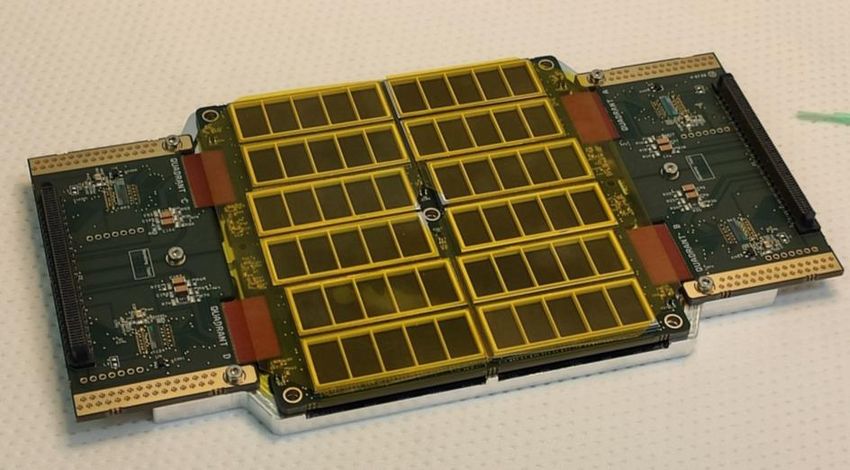
a field of view of several steradians and with arcmin-level accuracy, is gained by comparing time delays among the same
event detection epochs occurred on at least 3 nano-satellites. With a launch date in 2022, HERMES transient monitoring
represents a keystone capability to complement the next generation of gravitational wave experiments. In this paper we
will illustrate the HERMES payload design, highlighting the technical solutions adopted to allow a wide-energy-band
and sensitive X-ray and gamma-ray detector to be accommodated in a CubeSat 1U volume together with its complete
control electronics and data handling system.
Keywords: High Energy Astrophysics, HERMES, CubeSat, Payload, Space 4.0, Silicon Drift Detectors, GAGG, ASIC

                                                 1.   INTRODUCTION
HERMES (High Energy Rapid Modular Ensemble of Satellites) is a mission concept based on a constellation of nano-
satellites (3U CubeSats) in low Earth orbit, hosting innovative X and γ-ray detectors to probe the high-energy emission
of bright transients [1][2][3]. HERMES is built upon a twin project: the HERMES Technological Pathfinder (HERMES-
TP), funded by the Italian Ministry for education, university and research and the Italian Space Agency, and the
HERMES Scientific Pathfinder (HERMES-SP), funded by the European Union’s Horizon 2020 Research and Innovation
Programme under Grant Agreement No. 821896.
Both projects (HERMES-TP and HERMES-SP) provide three complete satellites (payload and service module) to the
constellation, aiming at demonstrating that fast GRB detection and localization is feasible with disruptive technologies
on-board miniaturized spacecrafts, mostly exploiting commercial off-the shelf (COTS) components at a cost 1–2 order of
magnitude lower than that of standard space projects (e.g. ESA M-class missions and NASA Explorer missions) and
with a development time of a just a few years. Moreover, the Italian Space Agency approved and funded the
participation to the SpIRIT (Space Industry – Responsive – Intelligent – Thermal Nanosatellite) CubeSat. The SpIRIT
project, which is supported by the Australian Space Agency and led by University of Melbourne, will host an HERMES-
like detector thus providing a seventh unit to the HERMES constellation.
The HERMES scientific goal is to demonstrates the accurate and prompt localization of bright hard X-ray/soft gamma-
ray transients such as Gamma-Ray Bursts (GRBs). Fast high-energy transients are among the likely electromagnetic
counterparts of the gravitational wave events (GWE) recently discovered by Advanced LIGO/Virgo [4], and of the Fast
Radio Bursts. Moreover, HERMES will open the window of X-ray timing down to a fraction of microseconds, and thus
investigate for the first time the temporal structure of GRBs at this scale to constrain models for the GRB engine and to
test quantum space-time scenarios by measuring the delay time between GRB photons of different energy.
Being based on cost-effective nanosatellites, HERMES is intrinsically a modular project. This allows to avoid single or
even multiple point failures (if one or several units are lost the constellation and the experiment is not lost) and to in-
flight test the hardware and on-board software with the first launches. If needed, both hardware and software can be
improved with the following launches.

                                    2.   HERMES PAYLOAD REQUIREMENTS
The flow-down of HERMES-TP and HERMES-SP Scientific Requirements [1] results in ambitious payload (P/L)
requirements: broad energy band, good efficiency, good energy resolution, high temporal resolution, extremely compact
design, reliable operation in a quite broad range of space environments (e.g., temperature, radiation damage, etc.).
Although these goals are certainly reachable on standard scientific experiments, an innovative and customized payload
design has been implemented in HERMES-TP/SP in order to fulfil the requirements in the limited mass, volume and
power resources of a CubeSat.
Given the required broad energy range, an integrated detector [5] has been designed to exploit a “double detection”
mechanism, with a partial overlap of the two detection systems around ~20 keV. Detection of soft X-rays (hereafter X-
mode) is obtained by a segmented solid state detector employing custom designed Silicon Drift Detector (SDD) [6], with
a cell size of about 0.45 cm2, which allows to attain a low noise level (of the order of a few tens of e - rms at room
temperature) and correspondingly a low energy threshold for the detection of X-ray radiation (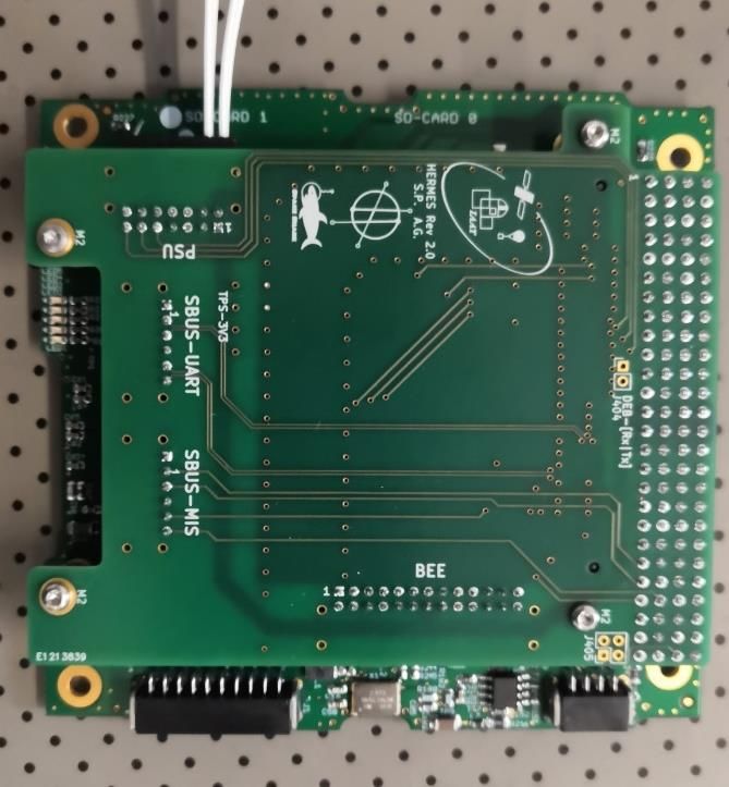
The discrimination between the two signals in the SDD (soft X-rays or optical photons) is achieved using the segmented
design: each scintillator crystal is read-out by two SDD cells, so that events detected in only one SDD are associated to
soft x-rays converted in a single SDD cell, while events detected simultaneously in more than one SDD are due to optical
light produced in the scintillator by an incoming hard X-ray/γ-ray. Table 1 summarizes the main HERMES-TP/SP
Payload Requirements.
Table 1 HERMES-TP/SP Payload requirements
Requirement Condition Value
E ≤ 20 keV (GRB short/long) ≤ 2 photons/s/cm2
Sensitivity
50 ≤ E ≤ 300 keV (GRB short/long) ≤ 1 photons/s/cm2
Energy band Elow ≤ 5 keV, Ehigh ≥ 500 keV
X-mode ≥ 50 cm2
Peak effective area
S-mode ≥ 50 cm2
Lower energy threshold ≤ 5 keV
5.0 – 6.0 keV ≤ 1 keV FWHM
Energy resolution EOL
50.0 – 60.0 keV ≤ 5 keV FWHM
X-mode ≤ 400 ns
Time resolution (1σ)
S-mode ≤ 250 ns
GPS locked ≤ 100 ns
Time accuracy (1σ)
GPS unlocked (up to 1500 s) ≤ 200 ns
Field of view ≥ 3 sr FWHM
Background rate 50–300 keV ≤ 1.5 counts/s/cm2
Background rate 20–300 keV ≤ 12 counts/s/cm2
Background knowledge ≤ 5%
Maximum sustainable GRB flux 40000 counts/s
On-board memory ≥ 16 Gbit
Mass allocation < 1.8 kg
Volume allocation ≤ 10 × 10 × 12.5 cm3 (1.25 U)
Power allocation ≤ 5W
Detector operative temperature range –30 °C ÷ +10 °C
P/L non operative temperature range –40 °C ÷ +80 °C
3. HERMES PAYLOAD DESIGN
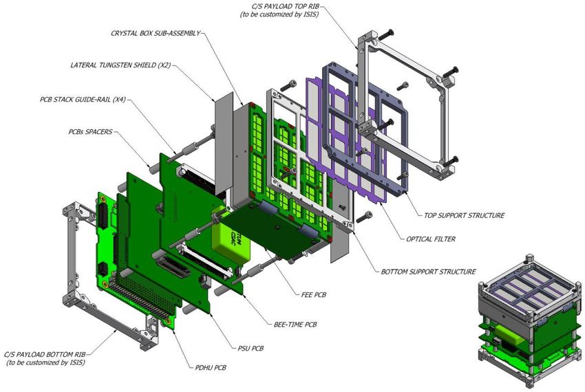
Figure 1 shows an exploded view of the HERMES-TP/SP payload. The payload is composed by 4 main subsystems: the
detector assembly (DA), the back-end electronic board (BEE), the power-supply electronic board (PSU) and the payload
data handling unit (PDHU). In the following we provide detailed description of each payload subsystem.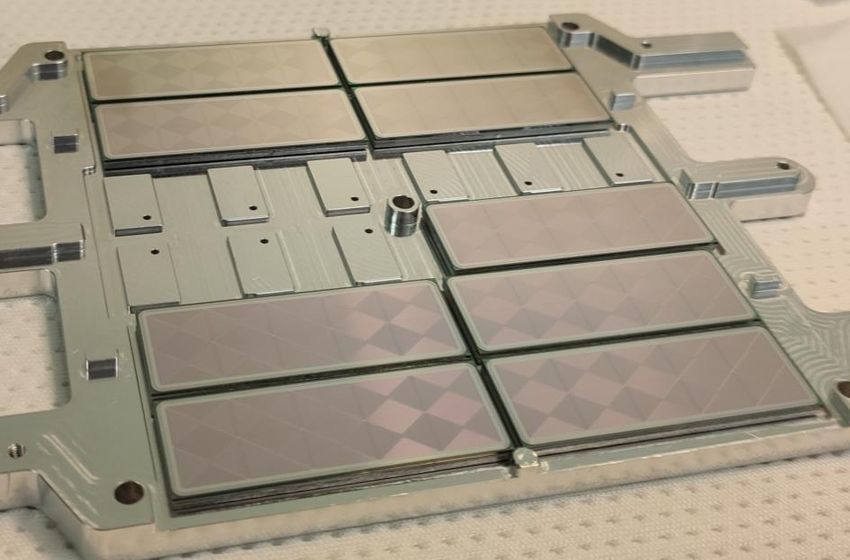
Figure 1 Exploded view of the HERMES-TP/SP P/L
3.1 Detector Assembly (DA)
The HERMES-TP/SP detector assembly [5] is composed of:
a detector support structure, mounted on the top of the sensitive plane. This structure is split in an upper and a
lower part, with an optical filter in-between;
a front-end electronics (FEE) board, a rigid-flex printed circuit board with a slotted main plate and two side
wings, connected to the main part with a flexible flat cable integrated in the board.
The FEE PCB hosts:
12 Silicon Drift Detector (SDD) arrays, each one with 10 independent cells, for a total of 120 detector
channels;
120 LYRA-FE ASIC dies, one for each SDD channel;
4 LYRA-BE ASICs, each one interfaced with 30 LYRA-FE channels;
discrete passive and active electronic components;
two electrical connectors (one per side) providing the electrical interfaces with the BEE board;
60 scintillator crystals, each one optically connected to two SDD cells. To maximize the optical contact
between SDD and crystal, ensuring optimal scintillation light readout, each crystal is:
o optically isolated on each side except the one in direct contact with the SDD, with a reflecting material;
o optically connected to the SDD through a transparent silicone layer;
o mechanically fixed inside satellite frame between the backside of the SDD box and the detector
support structure;
a crystal box, hosting the 60 scintillator crystal and providing the overall DA mechanical structure together
with the FEE board and the detector support structure. Three 200 m thick tungsten sheets are glued on the
bottom side and on two lateral sides of the crystal box to provide background shielding.
Figure 2 shows an exploded view of the HERMES-TP/SP DA.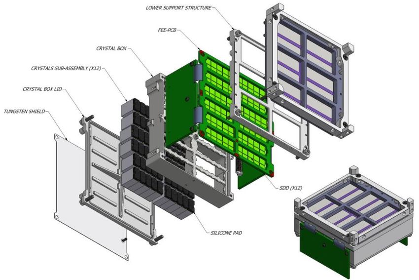
Figure 2 Exploded view of the HERMES-TP/SP Detector Assembly (DA)
As reported before, in order to reach a very wide energy band in an extremely compact instrument, the detector is based
on the so-called “siswich” concept [7][8]. In this architecture, the SDDs play the double role of read-out device for the
optical signal from the scintillator and of an independent X-ray solid state detector. The intrinsic low-noise
characteristics of the silicon drift technology allows reaching a low (< 20–30 keV) energy scintillator threshold. Above
these energies, the increasing sensitivity of the scintillator is able to compensate for the lack of efficiency of thin silicon
sensors, so a reasonably flat efficiency in a wide energy band for the whole integrated system is reached.
The HERMES SDDs are based on the state-of-the-art results achieved within the framework of the Italian ReDSoX
collaboration1, with the combined design and manufacturing expertise of INFN-Trieste and Fondazione Bruno Kessler
(FBK, Trento). Each SDD array (Figure 3) is composed by 25 cells on a 450 μm thick silicon substrate, with a cell of
7.44×6.05 mm2 for a total of 4.5 cm2 sensitive area. The whole matrix is surrounded by a 1.2 mm wide guard region
which allows for a correct electric field termination. The overall geometric area of the SDD array is 39.614.5 mm2. By
exploiting the single-side biasing technique [9], all the SDD bonding pads are placed on the detector n-side (i.e., the
anode side), thus providing a homogenous light entrance window for scintillation light readout. Four 500 μm wide
metallization strips are present on the p-side (optical window side) to ensure negligible optical crosstalk of the
scintillation light emitted by adjacent crystals.
1
http://redsox.iasfbo.inaf.it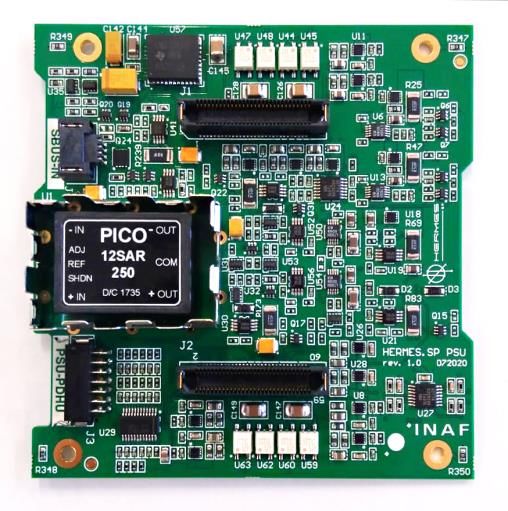
Figure 3 HERMES Silicon Drift Detectors (SDDs) on the detector integration jig
The scintillator are cerium-doped gadolinium-aluminum-gallium garnet crystals (Gd3Al2Ga3O12 or Ce:GAGG),
developed firstly in Japan around 2010, and commercially available since 2014 [10][11]. Ce:GAGG scintillators have
high intrinsic light output (~50000 photons/MeV), no intrinsic background, no hygroscopicity, fast radiation decay time
of ~90 ns, high density (6.63 g/cm3), peak light emission at 520 nm and high effective mean atomic number (54.4). All
these characteristics make the Ce:GAGG scintillators the optimal choice for the HERMES detector. The crystals have a
6.94 12.10 mm2 cross section and a 15 mm thickness, with chemically polished faces. Each crystal is optically coupled
to two adjacent SDD cells by means of a 3.3 mm thick Polydimethylsiloxane encapsulant (DOWSIL 93-500), allowing
for a reliable discrimination of X-ray and γ-ray photons via multiplicity analysis. The crystals are individually wrapped
with a 3M DF2000MA specular reflector film and grouped in sub-assemblies of five crystals, with one sub-assembly
coupled to an individual SDD array (Figure 4).
With the reported optical configuration, the crystal measured light output at room temperature is ~28 e-/keV, which
translates in ~14 e-/keV collected by each SDD channel reading-out the scintillator.
Figure 4 Ce:GAGG crystal optical assembly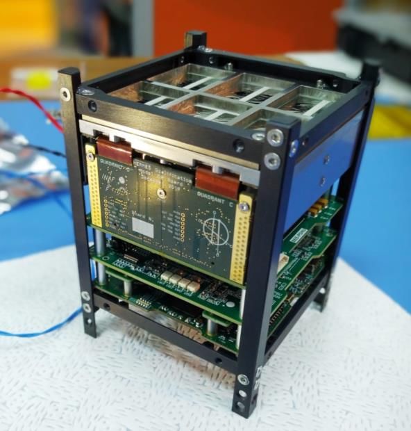
The Front-end electronics board (FEE, Figure 5) accommodates the 12 SDD matrices, 120 LYRA-FE ASICs, 4 LYRA-
BE ASICs, and several passive electronic components. The PCB is manufactured with a rigid-flex technology, allowing
the bending of the two side wings. Each wing hosts 2 LYRA-BE ASICs and a board-to-board connector providing the
FEE electrical interface with the back-end electronic board.
The 120 LYRA-FE chips are mounted on the top PCB layer, while the 12 SDD arrays are glued on the bottom PCB layer
by means of DOWSIL 3145 silicone adhesive. Aluminum wire bondings provide the electrical connection between the
ASICs and the FEE PCB (chip-to-board), the SDD biases (chip-to-board), and connection between the SDD anodes and
the LYRA-FE input pads (chip-to-chip).

    Figure 5 Demonstration model of the HERMES-TP/SP front-end PCB (FEE), integrated with 12 SDD arrays and LYRA-FE
                                          and LYRA-BE ASICs. See text for more details
The read-out ASIC design is based on the heritage of the VEGA ASIC [12][13], developed by Politecnico of Milano and
University of Pavia for the readout of large area SDD in the framework of the LOFT Phase-A study (ESA M3 Cosmic
Vision program).
In order to optimize the system noise performance, a distributed architecture has been adopted for the HERMES ASICs,
specifically designed and manufactured in AMS 0.35-µm CMOS mixed signal technology (Figure 6). The Front-End ICs
(LYRA-FE), which include the preamplifier, the first shaping stage and signal line-transmitter, are placed as near as
possible to each SDD anode. The current signal produced by the first-stage pulse shaper is transferred to one-channel of
the back-end IC (LYRA-BE), where it is collected by the current receiver block and further processed. Each LYRA-BE
can manage the signals produced by 30 LYRA-FE ICs, corresponding to one fourth of the HERMES-TP/SP detection
plane. Detailed description of the LYRA-FE and LYRA-BE ASICs can be found in [14][15].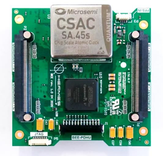
Figure 6 LYRA-FE ASICs (left) and LYRA-BE ASIC (right) integrated on the HERMES-TP/SP FEE PCB
The HERMES-TP/SP detector assembly is completed by an optical filter and an AISI 316 stainless steel structure
(Figure 7), which ensures the required mechanical stiffness to the FEE, encloses the Ce:GAGG crystals, and provide
background shielding (photons and particles) by means of 200 μm thick tungsten sheets glued on the bottom and on two
sides of the box containing the crystals. The top surface of each crystal is precisely aligned and held in position by means
of tips featured at the upper surface of the crystal box. Moreover, in order to compensate the CTE mismatch between
scintillators and crystal box and to withstand the dynamic forces acting on the scintillators during the ascending phases,
each crystal is preloaded with a 0.5 mm thick silicone layer placed between the scintillator bottom face and the crystal
box bottom lid.

     Figure 7 Left: Detector support structures (grey) and optical filter (purple). Right: Crystal box sub-assembly with wrapped
                                scintillators and DOWSIL 93-500 optical (top) and preload pads (bottom)

The optical filter of the HERMES-TP/SP detector is part of the optical design of the P/L. Its prime task is to prevent
NIR/O/UV light from reaching the SDD detector so to minimize the current noise generated by background photons with
energies larger than the Silicon bandgap. In addition, being the P/L thermal design based on passive cooling only, the
filter also enters the overall thermal design of the detector assembly. The HERMES-TP/SP filter has been manufactured
by the Institute of High Energy Physics (IHEP) of the Chinese Academy of Sciences (CAS) and consists of a 1 μm
polyimide layer with 200 nm Aluminum filming. A 100 μm thick nickel frame provide the filter mechanical stiffness and
the mounting interface with the detector support structure. As shown in Figure 8, a thickness of 1 μm for the Polyimide
and an Aluminum layer of 200 nm are acceptable from the point of view of transparency to X-rays, while guaranteeing
the required 10-7 absorption in the 102 nm – 105 nm wavelength range.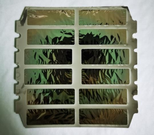
Figure 8 Left: Demonstration model of the HERMES-TP/SP filter manufactured by IHEP (Beijing). Right: Soft-X/UV/O/IR
          transmission of the optical filter estimated with different thickness of polyimide (1 µm and 2 µm) and different total
                 thickness of Al coating (200 nm and 300 nm) deposited on one or two sides of the polyimide substrate
3.2 Back-end electronic board (BEE)
The BEE (Figure 9) is the logic block between the front-end ASICs and the Payload Data Handling Unit. The BEE is in
charge of managing the ASICs configuration, the analog to digital conversion of the ASIC signals and the event time-
tagging exploiting the sub-microsecond accuracy of a local chip-scale atomic clock. Moreover, the BEE collects the
detector house-keeping data, commands the power lines required by the FEE, manages events data acquisition, transmits
science data and HKs to the PDHU as well as to receive and decode tele-commands sent by the PDHU.
The core of the BEE is a SEL immune Intel/Altera Cyclone V FPGA (5CEFA4F23I7N) that implements all the required
functions and tasks.

     Figure 9 Left: Demonstration model of the HERMES-TP/SP back-end electronics PCB. Right: schematic block diagram of
                                                          the BEE
The BEE receives, from the LYRA-BE ASICs, the analog event signals produced by the detectors and processed by the
front-end board electronics. The signal coming from each LYRA-BE is routed through a preamplifier/buffer to an
independent 12 bit, 1 MHz ADC, thus allowing for the simultaneous acquisition of the events detected in different
quadrants. With this architecture, the four detector quadrants behave as independent instruments, thus providing also
redundancy to the instrument.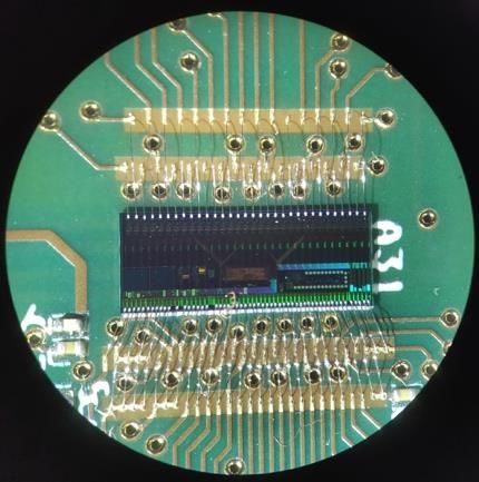
The BEE communicates with the PDHU through a serial line (SPI). All data exchanges are initiated by the PDHU
(master) through telecommands for writing, reading and task execution. The BEE receives and verifies the command and
executes the function commanded. The configuration of the LYRA-BE ASICs and of the payload operational modes are
transmitted by the PDHU under specific write commands. All the data acquired by the BEE (both scientific events and
housekeeping) are saved in a temporary buffer and transmitted to PDHU once per second. In case of substantial buffer
occupation, for example in presence of a high intensity astrophysical event, the BEE request an immediate data
transmission to the PDHU by activating a dedicated look-at-me digital line.
To generate the time reference for events time-tagging a combination of GPS Pulse per Second signal (PPS) from the
HERMS service module and a local ultra-stable clock is used. The ultra-stable clock is the space-qualified Microsemi
SA.45s chip-scale atomic clock (CSAC), which provides 1PPS and 10 MHz clock output signals with an accuracy of
±5.0E-11, a short-term Allan deviation lower than 10-11 (1000 s) and a typical aging rate of 910-10/month. The BEE
FPGA implements 2 counters: one incremented by the CSAC PPS (28 bits) and the other incremented by the 10 MHz
clock (24 bits). When the GPS signal is locked, the CSAC PPS signal is synchronized every second to the rising edge of
the PPS provided by the satellite bus, thus ensuring a continuous correction for the payload on-board time. In case of
GPS not locked, for example when the number of the GPS satellites tracked by the satellite bus GPS receiver is lower
than 4 due to the earth occultation, the CSAC still provides the 1PPS and 10 MHz clock signal in a free-running mode.
Exploiting this architecture, the HERMES-TP/SP expected timing performance are summarized in Table 2 and Table 3
for the GPS locked and unlocked cases respectively. For the GPS unlocked case (Table 3) an interval of 1500 s from the
last GPS lock has been considered.
Table 2 Time precision budget for the GPS locked case
Mode Time accuracy (68% c. l.) Time resolution (68% c. l.) Total (68% c. l.)
X-Mode 53.4 ns 320 ns 324 ns
S-mode 53.4 ns 216 ns 222 ns
Table 3 Time precision budget for the GPS unlocked case
Mode Time accuracy (68% c. l.) Time resolution (68% c. l.) Total (68% c. l.)
X-Mode 181 ns 320 ns 368 ns
S-mode 181 ns 216 ns 282 ns
3.3 Power Supply Unit (PSU)
Figure 10 Left: Demonstration model of the HERMES-TP/SP Power Supply Unit (PSU). Right: schematic block diagram of
the PSUA custom Power Supply Unit (PSU, Figure 10) board has been designed and manufactured to provide the power supplies
required by the payload (Figure 10). All the low voltages needed for the operation of the FEE are generated by ultra-low
noise linear Low Drop-Out (LDO) regulators. A DC-DC converter (Picoelectronics 12SAR250) is used for the
generation of the high-voltage detector biases while a Texas Instrument LMZ30602 is in charge of the generation of the
1.1V required by the BEE FPGA core.
The PSU receives from the satellite bus four power lines (12 V/80 mA, 5 V/100 mA and 23.3 V/1 A). Each line is
routed through electronic switches placed on the PSU board and commanded by the PDHU. Another set of switches are
placed in series with the main one and commanded by the BEE FPGA firmware.
All the low voltages lines are protected against overcurrent or latch-up in the powered circuitry by means of current
monitors which also provide alert lines routed to the BEE FPGA for latch-up monitoring and logging. Special care has
been taken in the PSU design to ensure a robust and safe latch-up control. In particular, a delay circuit is used to avoid
the protection activation due to inrush current, and two of sense amplifiers are implemented in parallel in a redundant
configuration for high reliability protection of sensitive power lines. Moreover, all the sense amplifiers are powered
downstream the sense resistor.
3.4 Payload Data Handling Unit (PDHU)
The HERMES-TP/SP Payload Data Handling Unit (PDHU) is the interface between the spacecraft and the payload. The
selected hardware for the PDHU is the Innovative Solutions In Space (ISIS) On-Board computer (iOBC). The iOBC is a
flight proven, high performance processing unit based around an ARM9 processor, and offers a multitude of
standardized interfaces. Combined with its daughterboard architecture, it allows for easy addition of mission specific
electronics or interfaces. A custom-made daughterboard is the current baseline for the PDHU system and provides all the
payload-bus electrical interfaces as well as the PHDU internal interface with the other payload subsystems.
Figure 11 Left: Engineering model of the HERMES-TP/SP Payload Data Handling Unit (PDHU) in the motherboard-
daughterboard configuration. Right: Schematic view of the P/L electrical interfaces provided by the PDHU
The electrical interfaces between the PDHU and the spacecraft are obtained by two harnesses connected to the PDHU
daughterboard (right panel in Figure 11), one providing the cables for the I2C protocol (devoted to direct TCs or
error/alarm reporting and power cycling the PDHU) and the LVTTL-RS232 UART (used to receive the GPS data), while
the other contains the lines for the UART TM/TC communication on a RS-422 bus.
The PDHU provides the payload central processing unit (CPU) and mass memory, and it is in charge of interfacing the
PSU for voltage line commanding, the BEE for internal TM/TC transmission and CSAC configuration, and the analog
temperature sensors of the payload for temperature monitoring and logging. Moreover, the PDHU manages the payload
operative modes, generates and filters the photon list, provides the formatting of the scientific and housekeeping data and
perform the burst trigger search. A detailed description of the HERMES-TP/SP PDHU and of its functionalities and
performance can be found in [16].4. PAYLOAD PERFORMANCE AND TECHNICAL BUDGETS
In the following, we present the preliminary payload performance as experimentally verified with the payload
demonstration model developed during the summer 2020.
4.1 Payload demonstration model
Figure 12 The HERMES-TP/SP PL demonstration model
A complete payload demonstration model (DM) has been built and tested in order to verify that the design of the system
fulfills the scientific and system requirements and to validate the AIV&T procedures. The DM has been integrated
during the months of August and September 2020 with a representative set of flight-like components, which includes: the
payload mechanical assembly completed of tungsten shields, the detector optical filter, the FEE board equipped with 4
LYRA-BE ASICs (one per DA quadrant), 120 LYRA-FE ASICs (30 per quadrant), 4 in-spec SDD arrays correspondent
to 40 FEE channels and 8 dummy SDD arrays, 60 GAGG crystals and a fully representative optical coupling and crystal
preload pads. The DM (Figure 12) is then completed by the three digital electronics boards (BEE, PSU, PDHU) which
are currently undergoing a complete test and characterization campaign.
4.2 Detector assembly DM characterization
In order to assess the X-mode and S-mode functionalities and preliminary performance, the integrated DA has been
characterized with radioactive sources at the IAPS Rome facility. The DA has been powered by means of unfiltered
laboratory power supplies connected, through an adapter board, directly to the LYRA-BE and LYRA-FE ASIC and to
the SDD bias network. The LYRA-BE ASICs command and communication tasks have been managed by means of a
FPGA-based commercial board (Arty Z7) and a custom developed software and firmware. The output analog signals
have been readout using a commercial multi-channel fast ADC (CAEN DT5740) and analyzed using specifically
developed algorithms in IDL and Python languages.
A series of energy spectra have been acquired at +26 °C and +5 °C by illuminating the detector simultaneously with X-
rays (55Fe and 109Cd) and γ-rays (137Cs) sources. Figure 13 reports the distribution of the DM X-mode energy resolution
(at 5.9 keV, Mn Kα fluorescence line) experimentally measured with a detector leakage current consistent with the end-
of-life (EOL) expected current due to the radiation damage. As it can be seen, the system shows an overall noise
performance well below the required resolution of 1 keV FWHM EOL reported in Section 2. Moreover, the limited noise
allows for a low energy threshold setting lower than 2.5 keV for all the DM channels, as shown in Figure 14.Figure 13 Demonstration model energy resolution at 5.9 keV measured with EOL equivalent detector leakage current
Figure 14 Demonstration model lower energy threshold measured with EOL equivalent detector leakage current
Figure 15 Single channel light output measured at T= +5 °C at 662 keV
Figure 15 shows the distribution of the single channel light output measured with the HERMES-TP/SP DM silicon drift
detectors at a temperature of +5° C at 662 keV with a 137Cs radioactive source. The average light output is 13.7 e-/keV
(which corresponds to 27.4 e-/keV for each Ce:GAGG crystal), with a standard deviation of 0.5 e-/keV. More details
about the DM measured performance for both the X-mode and S-mode can be found in [5].4.3 Demonstration model environmental testing
The HERMES-TP/SP P/L mechanical and thermal models have been validated by means of random vibration test and
thermal balance test performed at the Politecnico di Milano facilities at the beginning of October 2020.
The DM has been successfully tested with the sine and random vibration levels reported in Table 4 and Table 5
respectively.
Table 4 Sine vibration test levels
Axis Frequency [Hz] Qualification level
5–75 2.5 g
Out of plane/In plane 75–110 1.25 g
110–125 0.25 g
Sweep rate 2 Oct/min 1 sweep up
Table 5 Random vibration tests levels
Frequency [Hz] Level [G2/Hz]
20 0.0224
50 0.0224
100 0.0449
200 0.1122
500 0.1122
1000 0.0449
2000 0.0224
Overall 10.6 Grms
Duration 2 minutes
The thermal balance test (TBT) has been performed to provide data for the verification of the thermal mathematical
model as part of the thermal control subsystem qualification, and to provide information about the sensitivity of the
thermal control subsystem design with respect to parameter changes. The conditions of the thermal balance set points are
reported in Table 6. The number of steady states (6) has been chosen following the ECSS prescriptions.
Table 6 Thermal balance test conditions
Test condition Condition
Reference balance 0 °C
Cold balance –25 °C
Hot balance +30 °C
Set point tolerance ±3 °C
Temperature slew rate5. CONCLUSIONS
In this paper we presented the design, development and preliminary performance characterization of the HERMES-
TP/SP payload, devoted to the study and fast localization of high energy transients with sub-microsecond time resolution
and a wide energy band, spanning from few keV up to 2 MeV. A demonstration model has been assembled and tested to
validate the payload mechanical and thermal design, as well as to perform the payload requirement verification. The P/L
critical design review (CDR) has been successfully passed on October/November 2020. Assembly, integration and test
activities (both functional and environmental) of the first payload proto flight module (PFM) is foreseen for Q1/Q2 2021.
Production and test of the other five flight modules (FMs) will follow, ending in Q4 2021.
Table 7 summarizes the technical and performance budgets of the HERMES-TP/SP P/L as measured during the
characterization of the payload demonstration model, while detailed studies of the HERMES-TP/SP space environment
and of the instrument in-flight performance can be found in [17], [18], [19] and [20].
Table 7 Technical and performance budget of the HERMES-TP/SP payload
Parameter Value
Payload peak effective area (X-mode & S-mode) 52 cm2
Field of View 3.2 sr FWHM
Lower energy threshold ≤ 3 keV
Energy resolution X-mode (@ 6 keV) ≤ 800 eV FWHM
Energy resolution S-mode (@ 60 keV) ≤ 5 keV FWHM
Time resolution (68% c.l.) 320 ns
Time accuracy (68% c.l.) 181 ns
Payload mass 1588 g
Payload power in Observation 4791 mW
Payload Telemetry (scientific + engineering) 719 Mbits/day
ACKNOWLEDGMENTS
This work has been carried out in the framework of the HERMES-TP and HERMES-SP collaborations. We
acknowledge support from the European Union Horizon 2020 Research and Innovation Framework Programme under
grant agreement HERMES-Scientific Pathfinder n. 821896 and from ASI-INAF Accordo Attuativo HERMES
Technologic Pathfinder n. 2018-10-H.1-2020.
REFERENCES
[1] Fiore, F. et al., “The HERMES-Technologic and Scientific Pathfinder”, Society of Photo-Optical
Instrumentation Engineers (SPIE) Conference Series, 11444-166 (2020)
[2] Sanna, A. et al., “Timing techniques applied to distributed modular high-energy astronomy: the H.E.R.M.E.S.
project”, Society of Photo-Optical Instrumentation Engineers (SPIE) Conference Series, 11444-251 (2020)
[3] Burderi, L. et al., “GrailQuest & HERMES: Hunting for Gravitational Wave Electromagnetic Counterparts and
Probing Space-Time Quantum Foam”, Society of Photo-Optical Instrumentation Engineers (SPIE) Conference
Series, 11444-252 (2020)
[4] Abbott, B. P. et al., “Multi-messenger Observations of a Binary Neutron Star Merger”, The Astrophysical
Journal Letters, 848, L12 (2017)
[5] Fuschino, F. et al., “An innovative architecture for a wide band transient monitor on board the HERMES nano-
satellite constellation”, Society of Photo-Optical Instrumentation Engineers (SPIE) Conference Series, 11444-
167 (2020)[6] Gatti, E. and Rehak, P., “Semiconductor drift chamber - an application of a novel charge transport scheme,”
Nuclear Instruments and Methods in Physics Research 225, 608 – 614 (1984)
[7] Marisaldi, M., Labanti, C., and Soltau, H., “A pulse shape discrimination gamma-ray detector based on a silicon
drift chamber coupled to a csi(tl) scintillator: prospects for a 1 kev-1 mev monolithic detector,” IEEE
Transactions on Nuclear Science 51, 1916–1922 (2004).
[8] Marisaldi, M., Labanti, C., Fuschino, F., and Amati, L., “A broad energy range wide field monitor for next
generation gamma-ray burst experiments,” Nuclear Instruments and Methods in Physics Research, 588, 37–40
(2008).
[9] Fiorini, C. et al, “Single-side biasing of silicon drift detectors with homogeneous light-entrance window”, IEEE
Transaction on Nuclear Science, 47, 1691–1695 (2000)
[10] Kamada, K. et al., “Crystal growth and scintillation properties of Ce doped Gd3(Ga, Al)5O12 single crystals”,
IEEE Transactions on Nuclear Science 59, 2112–2115 (2012)
[11] Yoneyama, M. et al., “Evaluation of GAGG:Ce scintillators for future space applications”, Journal of
Instrumentation, 13, 02, P02023 (2018)
[12] Ahangarianabhari, M. et al., “Vega: A low-power front-end asic for large area multi-linear x-ray silicon drift
detectors: Design and experimental characterization”, Nuclear Instruments and Methods in Physics Research,
770, 155–163 (2015)
[13] Campana, R. et al., “Characterization of the VEGA ASIC coupled to large area position-sensitive silicon drift
detectors,” Journal of Instrumentation, 9, P08008 (2014)
[14] Gandola, M. et al., “LYRA: A Multi-Chip ASIC Designed for HERMES X and Gamma Ray Detector,” in IEEE
Nuclear Science Symposium and Medical Imaging Conference (NSS/MIC), 1–3 (2019)
[15] Grassi, M. et al., “X-/γ-Ray Detection Instrument for the HERMES Nano-Satellites Based on SDDs Read-Out
by the LYRA Mixed-Signal ASIC Chipset”, in IEEE International Instrumentation and Measurement
Technology Conference (I2MTC), 1–6 (2020)
[16] Guzman, A. et al., “The Payload Data Handling Unit (PDHU) on-board the HERMES-TP and HERMES-SP
CubeSat Missions”, Society of Photo-Optical Instrumentation Engineers (SPIE) Conference Series, 11444-254
(2020)
[17] Campana, R. et al., “The HERMES-TP/SP background and response simulations”, Society of Photo-Optical
Instrumentation Engineers (SPIE) Conference Series, 11444-248 (2020)
[18] Dilillo, G. et al., “A summary on an investigation of GAGG:Ce afterglow emission in the context of future
space applications within the HERMES nanosatellite mission”, Society of Photo-Optical Instrumentation
Engineers (SPIE) Conference Series, 11444-185 (2020)
[19] Galgóczi, G. et al., “A software toolkit to simulate activation background for high energy detectors onboard
satellites”, Society of Photo-Optical Instrumentation Engineers (SPIE) Conference Series, 11444-184 (2020)
[20] Ripa, J. et al., “A comparison of trapped particle models in low Earth orbit”, Society of Photo-Optical
Instrumentation Engineers (SPIE) Conference Series, 11444-74 (2020)You can also read