Towards practical applications of quantum emitters in boron nitride
←
→
Page content transcription
If your browser does not render page correctly, please read the page content below
www.nature.com/scientificreports
OPEN Towards practical applications
of quantum emitters in boron
nitride
M. Koperski1*, K. Pakuła2, K. Nogajewski2, A. K. Dąbrowska2, M. Tokarczyk2, T. Pelini3,
J. Binder2, T. Fąs2, J. Suffczyński2, R. Stępniewski2, A. Wysmołek2 & M. Potemski2,3
We demonstrate quantum emission capabilities from boron nitride structures which are relevant
for practical applications and can be seamlessly integrated into a variety of heterostructures and
devices. First, the optical properties of polycrystalline BN films grown by metalorganic vapour-phase
epitaxy are inspected. We observe that these specimens display an antibunching in the second-order
correlation functions, if the broadband background luminescence is properly controlled. Furthermore,
the feasibility to use flexible and transparent substrates to support hBN crystals that host quantum
emitters is explored. We characterise hBN powders deposited onto polydimethylsiloxane films, which
display quantum emission characteristics in ambient environmental conditions.
One of the domains in photonics, constantly growing in relevance for contemporary and future communication
technologies, is the generation of light that displays quantum qualities. The ability to procure, with high prob-
ability, an individual photon creates an opportunity to manipulate a state of a fundamental quantum system for
the benefit of secure information carriage at the highest attainable speed. At present, various quantum emitters
are investigated and considered for possible applications. The family of well-established quantum light sources,
such as isolated semiconductor quantum dots1,2, single molecules3,4 and individual crystal defects5,6, has recently
incorporated the emitting centres in thin layers of 2D m aterials7–11. The marriage of 2D world with quantum
emitters is particularly appealing from the point of view of practical aspects. With constant advancements of
fabrication procedures, it is feasible to design and create heterostructures which combine materials exhibiting a
variety of optical and electrical properties. The selection of functionalities offered by thin films of 2D materials
includes now generation of single photons.
Among 2D materials that host quantum emitters, hexagonal boron nitride (hBN) appears as an especially
promising candidate which could fulfil many requirements for a practically useful single photon source. The
emergent defect-related emitters give rise to photoluminescence in form of spectrally narrow lines11–20, which
cover an exceptionally broad energy range, from near-infrared to ultraviolet optical regions. Such deep-level
centers can constitute pure quantum systems, unperturbed by hybridization effects with fundamental electronic
bands. The second-order photon correlation functions obtained for individual emission resonances reveal a
good quality antibunching demonstrating quantum emission capabilities in cryogenic conditions and at room
temperature. The samples investigated so far have been based mostly on commercially available hBN powders or
thin hBN films mechanically exfoliated from bulk c rystals13 or grown via d eposition21 or e pitaxy22,23 techniques.
Most of these efforts are tailored towards achieving single crystal materials that host controllable defects. The
inspection of the optical response of the emergent quantum emitters in a well-defined crystallographic environ-
ment is essential for achieving fundamental understanding of the optoelectronic properties originating from
fundamental sub-bands and defect-induced midgap l evels24. However, ample modern technologies rely on poly-
crystalline films and/or structures, hence the development of useful quantum emitters needs to take such tech-
nological challenges into account. Particularly, technological progress will require utilization of crystal growth
techniques that are scalable and allow high-throughput fabrication of crystals that display quantum emission.
Here, we explore the metalorganic vapour-phase epitaxy (MOVPE) techniques for fabricating hBN layers when
we relax the condition of obtaining high-quality single crystals to accelerate the growth rate and efficiency while
maintaining quantum emission capabilities.
1
Department of Materials Science and Engineering, National University of Singapore, Singapore 117575,
Singapore. 2Faculty of Physics, University of Warsaw, Pasteura 5, 02‑093 Warsaw, Poland. 3Laboratoire National
des Champs Magnétiques Intenses, CNRS-UGA-UPS-INSA-EMFL, Grenoble, France. *email: msemaci@
nus.edu.sg
Scientific Reports | (2021) 11:15506 | https://doi.org/10.1038/s41598-021-93802-8 1
Vol.:(0123456789)
www.nature.com/scientificreports/
Carrier gas Reactor pressure (mbar) NH3 volume (cm3) Estimated BN layer thickness (nm)
S1 H2 600 2000 800
S2 N2 600 1000 1250
S1 H2 100 100 550
Table 1. The set of MOVPE growth parameters used to grow thick layers of polycrystalline hBN with crystals
of various geometries. See S. I., Fig. S1 for example SEM images.
From the point of view of optical characterisation of quantum light sources in hBN, the spectral properties
of such emitters are quite well understood. Further progress in the field will likely depend on a possibility to
tailor the parameters of the hBN samples and to realise novel ideas for incorporation of hBN quantum emitters
into structures of practical importance. In this work we explore these concepts by (i) characterising the hBN
samples grown by the method of MOVPE when using different process parameters and (ii) demonstrating that
hBN powder emitters may act as efficient quantum emitters on flexible and transparent polydimethylsiloxane
(PDMS) films in ambient atmosphere. The reported observations are relevant for the progress in development
of technologically sound BN structures with the focus on quantum emission capabilities in a broad range of
environmental conditions.
Quantum emitters in MOVPE‑grown polycrystalline hBN structures
hBN polycrystalline films have been grown via MOVPE on sapphire supports using process parameters as listed
in Table 1. For the optical study, the hBN structures were relocated onto Si/SiO2 substrates via pick-up transfer
techniques utilising polydimethylsiloxane membranes. Generally, the photoluminescence (PL) spectra of our
MOVPE hBN samples measured under conditions of the below bandgap excitation take form of broad emission
bands. Such response of wide gap materials in visible spectral range may be related to ensembles of deeply bound
defect states. Most importantly, the high-resolution μPL mapping reveals locations where individual narrow emis-
sion lines arise. Although all investigated samples reveal such narrow line emitters, the potential to isolate single
PL resonances is limited by the apparent intensity of the broadband contribution. Representative spectra for
samples S1–S3, showing signature of individual quantum emitters in our MOVPE hBN, are presented in Fig. 1.
It is quite clear that the feasibility of an observation of individual defects in the optical spectra varies strongly
across the investigated samples. Interestingly, the intensity of the background appears to be mostly related to the
character of the crystallites that form the hBN layers, as may be seen in scanning electron microscopy images
shown in Fig. S1 in Supplementary Information.
A general inspection of the properties of quantum emitters in the MOVPE-grown hBN shows similar charac-
teristics to those displayed by their counterparts in mechanically exfoliated layers and p owders11–15. Representa-
tive results of the optical characterisation of the narrow line emitting centres in our samples are summarised
in Fig. 2. Individual emitters exhibit a large degree of linear polarization of emitted light, which is indicative of
an intrinsic anisotropy of the states partaking in the recombination processes. The angular dependence of the
emission intensity is given as:
I(α) = IA (sin (α − α0 ))2 + I0
Here, IA is the amplitude of the angle (α)-dependent oscillations, α0 is the phase shift with respect to an arbitrar-
ily chosen axis of the linear polarizer and I0 is the minimal intensity (displayed by the emitter when intrinsic
polarisation axis is perpendicular to the axis of the polarizer). The luminescent centre, whose emission spectra
and angle-dependent emission intensity is presented in Fig. 2a,b, displays a polarisation degree of:
Imax − Imin IA
Pdeg = = = 37 ± 1%.
Imax + Imin IA + 2I0
Characteristically for hBN quantum emitters, the second-order correlation function, obtained in Hanbury
Brown and Twiss configuration, is dominated by a short time-scale antibunching25 in combination with a longer
time-scale bunching. The shape of the bunching can be reproduced well by a bi-exponential decay function, so
that the experimental data is well accounted for by the following formula:
−|τ |/ −|τ |/ −|τ |/
g (2) (τ ) = A1 e t1 + A2 e t2 − A3 e t3 + 1
with characteristic times t1 = 1.3 ± 0.1 µs , t2 = 77 ± 1 µs , t3 = 1.2 ± 0.3 ns and bunching amplitudes
A1 = 1.1 ± 0.1, A2 = 0.3 ± 0.1. The emergent anti-bunching is characterised by an amplitude that constitutes
70 ± 3% of the maximum number of counts.
The parameters describing the g (2)(τ) function can also be altered by varying the excitation conditions. Fig-
ure 3 presents the dependence of the photoluminescence spectra and the correlation functions on the excitation
power. Comparatively, this data demonstrates the decrease of the broadband background emission in the time-
integrated spectra in conjunction with the decrease of the bunching amplitude for lower excitation powers. These
two effects consequently decrease the value of g(2)(0). Particularly, in the regime of low excitation power (0.1 mW
focused to a spot of about a micron diameter in our experiment), the broadband background contribution and
Scientific Reports | (2021) 11:15506 | https://doi.org/10.1038/s41598-021-93802-8 2
Vol:.(1234567890)
www.nature.com/scientificreports/
Figure 1. The optical images of Si/SiO2 substrates supporting transferred MOVPE hBN are confronted with
typical μPL spectra taken on locations displaying emission from single defects for samples S1 (a,b), S2 (c,d) and
S3 (e,f), respectively. The low temperature (5 K) μPL spectra were measured under 514 nm laser excitation with
the power on the sample 300 μW for samples S1, S2 and 50 μW for sample S3. All studied samples host quantum
emitters. However, for the specimen with strong broadband background it is infeasible to find suitable excitation
conditions (e.g., resonant laser energy or linearly polarised excitation aligned with the intrinsic anisotropy axis
of the emitter13), so that the narrow lines would be well pronounced (sample S3).
the bunching effect are negligible. The parameters of the correlation function relevant for the quantum emission
capabilities of this emitter are presented in Table 2.
Quantum emitters in hBN powders on a flexible and transparent substrate
The appearance of quantum emitters in different forms of hBN, especially the polycrystalline structures, allows
their seamless integration with a variety of modern technologies. Particularly important are optoelectronic struc-
tures and devices operating on transparent and/or flexible substrates26–28. Here, we demonstrate the quantum
emission capabilities of hBN powders deposited onto polydimethylsiloxane (PDMS) films. Our micro-optical
characterisation of such samples provides a proof of concept that quantum emitters in hBN may operate in ambi-
ent conditions on polymer films in a comparable fashion as on commonly used non-conductive crystal substrates.
In Fig. 4, we present a comparison between the room- and cryogenic-temperature optical response of the
hBN powder deposited on a PDMS film under 2.410 eV (514.4 nm) laser excitation. In both cases, a doublet of
Raman lines from PDMS p olymer29 is conspicuous around 2920 cm−1 combined with a narrower hBN Raman
resonance at 1356 cm−1. In the room temperature spectrum, presented in Fig. 4a, an additional broader line
appears at 2.288 eV. At low temperature, the hBN emission resonances become significantly narrower, demon-
strating that PDMS film may transfer heat efficiently even at cryogenic conditions, consequently allowing the
hBN powder to thermalize.
In Fig. 4c, the most robust additional narrow resonances are seen at 1.843 eV and 2.269 eV. More examples of
photoluminescence spectra, illustrating a broad spectral range wherein emission resonances from hBN powder
may be found, are presented in S. I. in Fig. S3. A very good stability on the timescale of hundreds of seconds is
Scientific Reports | (2021) 11:15506 | https://doi.org/10.1038/s41598-021-93802-8 3
Vol.:(0123456789)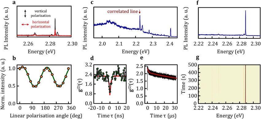
www.nature.com/scientificreports/
Figure 2. The low temperature (5 K) optical properties of the MOVPE-grown hBN. (a) The photoluminescence
spectra resolved by the linear polarisation along two mutually perpendicular axes demonstrate that individual
emission resonances display the high degree of linear polarisation (37 ± 1%). (b) A systematic dependence of the
emission intensity of the most intense line in the spectrum may be reproduced by a squared sinusoidal function.
Our individual BN emitters act as quantum emitters as presented for the resonance indicated in (c) in form of
photon correlation function depicted (d) at shorter and (e) longer timescale. The stability of individual emission
lines is very good for most emitters. This can be seen, e.g., for well-isolated resonances in (f), in a colour maps
representing temporal evolution of the spectrum presented in (g).
Figure 3. The power dependence of (a) the photoluminescence spectra obtained under 2.33 eV laser
illumination in microscopic configuration at 1.8 K demonstrates the controllability of the broadband emission
by the excitation conditions. Varying excitation power also impacts the bunching and antibunching amplitudes
as seen in the g(2)(τ) functions for (b) 4 mW, (c) 2 mW and (d) 0.1 mW excitation power.
observed for the hBN emission resonances in both ambient and low temperature experiments, as revealed by
the temporal evolution of the optical spectra demonstrated in Fig. 4b,d.
The most relevant for practical aspects of a useful quantum emitter is the presence of an antibunching in
photon correlation function in ambient conditions. It is indeed observable for the individual emission reso-
nances displayed by hBN powder on PDMS samples, as we demonstrate in Fig. 5. Notably, the quantum emission
Scientific Reports | (2021) 11:15506 | https://doi.org/10.1038/s41598-021-93802-8 4
Vol:.(1234567890)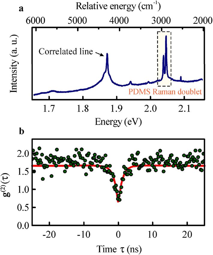
www.nature.com/scientificreports/
Laser power (mW) Bunching amplitude (A1) Antibunching amplitude ( A3) g(2)(0)
4 0.41 ± 0.01 1.10 ± 0.04 0.31 ± 0.05
2 0.24 ± 0.01 0.98 ± 0.03 0.26 ± 0.04
0.1 0 0.86 ± 0.04 0.14 ± 0.04
Table 2. The fitting results for the experimental g(2)(τ) functions from Fig. 3 are presented. For this data,
A2 parameter was set to 0 as the bunching shape could be reproduced with a single time constant. The other
parameters were fitted with the exception of bunching amplitude for the g (2)(τ) function obtained under the
condition of 0.1 mW laser excitation, for which the bunching amplitude is negligible.
Figure 4. The optical response of hBN powder deposited onto PDMS films is presented at room temperature
(a) and low temperature (c) conditions. The additional emission resonances accompany the PDMS Raman
doublet and hBN optical phonon resonances. The hBN emission lines (e.g., that at 1.843 eV) display good
stability at both cryogenic and ambient conditions as presented in the temporal evolution colour maps in (b,d).
from the hBN material is persevered under conditions suitable for practical operation of flexible optoelectronic
devices. With PDMS being commonly used in exfoliation t echniques30, a development of simple cavity s ystems31
or waveguides32,33, its combination with hBN powders creates an opportunity to utilize single photon sources
in creative ways.
Summary
We have explored technological aspects of utilising hBN quantum emitters as building blocks compatible with
a broad range of modern technologies. Our MOVPE polycrystalline BN films display well-isolated and robust
narrow-line resonances characterised by deep antibunching in a second-order correlation function. Such observa-
tion demonstrates that high-quality solid-state single quantum emitters do not necessarily require high-quality
single crystals. Furthermore, there appears to be no stringent requirements for the substrates in order to achieve
quantum emission from hBN structures in ambient conditions. As a proof of principle, we verify this notion by
inspecting the optical response of quantum emitters in hBN on PDMS films, which may play a pivotal role in
fabrication of 2D heterostructures and devices.
Methods
Crystal growth. The BN crystals were grown on two-inch sapphire wafers via MOVPE method using an
Aixtron CCS 3 × 2″ system. Triethylborane ( C6H15B, TEB) and ammonia ( NH3) were used as the active agents
acting as a source of boron and nitrogen, respectively. The growth temperature was controlled in situ by ARGUS
Thermal Mapping System and for all samples was set to 1050 °C. The differences between the studied samples
arise from the variation of growth parameters: carrier gas (nitrogen or hydrogen), reactor pressure and the vol-
ume of ammonia. The dependence of the properties and surface morphology on growth parameters has been
Scientific Reports | (2021) 11:15506 | https://doi.org/10.1038/s41598-021-93802-8 5
Vol.:(0123456789)www.nature.com/scientificreports/
Figure 5. Room temperature quantum emission from hBN powder deposited onto PDMS film. The emission
resonance used in second-order correlation function measurements is located at 1.872 eV as demonstrated
in the optical spectrum (a) under 2.41 eV (514.4 nm) laser excitation. The g (2) (τ ) function displays an
antibunching with the depth given by the amplitude that constitutes 62 ± 2% of the maximum number of counts.
further described in Ref. 34. All samples were grown in the conditions of ammonia insufficiency which promotes
not only formation of nitrogen vacancies but also carbon incorporation into the boron nitride structure. Such
growth strategies may open new pathways for controllable formation of specific luminescent centres. Relatively
large amount of TEB results in a very effective material synthesis. Dense nucleation on the sapphire surface and
appearance of defects during the growth rule out formation of epitaxial, continuous layer well aligned with the
sapphire substrate and for this reason obtained boron nitride has a polycrystalline form.
Sample preparation. The MOVPE-grown BN layers were transferred from the initial sapphire substrates
to commonly used in optical spectroscopy Si/SiO2 substrates, allowing better visualisation of the BN layered
via optical contrast methods. PDMS-based pick-up transfer technique was used to relocate the boron nitride
crystals between various supports.
Optical spectroscopy. The optical spectra were measured in a standard back-scattering geometry under a
single-frequency 514.4 nm (2.410 eV) laser excitation. The laser beam was focused on the surface of the sample
down to a spot of about 1 μm diameter with a long working distance 50 × magnification objective. The signal
from the sample was spectrally resolved with a 500 mm spectrometer and detected by a charge-coupled device
camera, producing an optical spectrum which consists of a combination of Raman and photoluminescence
resonances. A flow helium cryostat equipped with a cold finger was used to cool the samples down to 5 K tem-
perature. The optical spectra resolved by the linear polarisation were measured with a λ/2 waveplate followed by
a linear polarised located in the detection path of the optical setup.
The photon correlation measurements were performed in a Hanbury Brown and Twiss configuration with the
continuous wave 514.4 nm laser acting as an excitation source. Two avalanche photodiodes with a response time
of 200 ps were used to detect the single photons and generate electrical signals. The delay between the electrical
pulses was measured with a specialised correlation card module.
Received: 8 January 2021; Accepted: 25 June 2021
Scientific Reports | (2021) 11:15506 | https://doi.org/10.1038/s41598-021-93802-8 6
Vol:.(1234567890)www.nature.com/scientificreports/
References
1. Reed, M. A. et al. Observation of discrete electronic states in a zero-dimensional semiconductor nanostructure. Phys. Rev. Lett.
60, 535–537. https://doi.org/10.1103/PhysRevLett.60.535 (1988).
2. Michler, P. et al. A quantum dot single-photon turnstile device. Science 290, 2282. https://doi.org/10.1126/science.290.5500.2282
(2000).
3. Brunel, C., Lounis, B., Tamarat, P. & Orrit, M. Triggered source of single photons based on controlled single molecule fluorescence.
Phys. Rev. Lett. 83, 2722–2725. https://doi.org/10.1103/PhysRevLett.83.2722 (1999).
4. Lounis, B. & Moerner, W. E. Single photons on demand from a single molecule at room temperature. Nature 407, 491–493. https://
doi.org/10.1038/35035032 (2000).
5. Gruber, A. et al. Scanning confocal optical microscopy and magnetic resonance on single defect centers. Science 276, 2012. https://
doi.org/10.1126/science.276.5321.2012 (1997).
6. Mizuochi, N. et al. Electrically driven single-photon source at room temperature in diamond. Nat. Photonics 6, 299–303. https://
doi.org/10.1038/nphoton.2012.75 (2012).
7. Srivastava, A. et al. Optically active quantum dots in monolayer WSe2. Nat. Nanotechnol. 10, 491–496. https://doi.org/10.1038/
nnano.2015.60 (2015).
8. Chakraborty, C., Kinnischtzke, L., Goodfellow, K. M., Beams, R. & Vamivakas, A. N. Voltage-controlled quantum light from an
atomically thin semiconductor. Nat. Nanotechnol. 10, 507–511. https://doi.org/10.1038/nnano.2015.79 (2015).
9. He, Y.-M. et al. Single quantum emitters in monolayer semiconductors. Nat. Nanotechnol. 10, 497–502. https://doi.org/10.1038/
nnano.2015.75 (2015).
10. Koperski, M. et al. Single photon emitters in exfoliated W Se2 structures. Nat. Nanotechnol. 10, 503–506. https://doi.org/10.1038/
nnano.2015.67 (2015).
11. Tran, T. T., Bray, K., Ford, M. J., Toth, M. & Aharonovich, I. Quantum emission from hexagonal boron nitride monolayers. Nat.
Nanotechnol. 11, 37–41. https://doi.org/10.1038/nnano.2015.242 (2016).
12. Martínez, L. J. et al. Efficient single photon emission from a high-purity hexagonal boron nitride crystal. Phys. Rev. B 94, 121405.
https://doi.org/10.1103/PhysRevB.94.121405 (2016).
13. Koperski, M., Nogajewski, K. & Potemski, M. Single photon emitters in boron nitride: More than a supplementary material. Opt.
Commun. 411, 158–165. https://doi.org/10.1016/j.optcom.2017.10.083 (2018).
14. Toth, M. & Aharonovich, I. Single photon sources in atomically thin materials. Annu. Rev. Phys. Chem. 70, 123–142. https://doi.
org/10.1146/annurev-physchem-042018-052628 (2019).
15. Pelini, T. et al. Shallow and deep levels in carbon-doped hexagonal boron nitride crystals. Phys. Rev. Mater. 3, 094001. https://doi.
org/10.1103/PhysRevMaterials.3.094001 (2019).
16. Koperski, M. et al. Midgap radiative centers in carbon-enriched hexagonal boron nitride. Proc Natl. Acad. Sci. 2020(117), 13214–
13219. https://doi.org/10.1073/pnas.2003895117 (2020).
17. Mackoit-Sinkevičienė, M., Maciaszek, M., Van de Walle, C. G. & Alkauskas, A. Carbon dimer defect as a source of the 4.1 eV
luminescence in hexagonal boron nitride. Appl. Phys. Lett. 115, 212101. https://doi.org/10.1063/1.5124153 (2019).
18. Grosso, G. et al. Low-temperature electron–phonon interaction of quantum emitters in hexagonal boron nitride. ACS Photonics
7, 1410–1417. https://doi.org/10.1021/acsphotonics.9b01789 (2020).
19. Sajid, A., Ford, M. J. & Reimers, J. R. Single-photon emitters in hexagonal boron nitride: A review of progress. Rep. Prog. Phys. 83,
044501. https://doi.org/10.1088/1361-6633/ab6310 (2020).
20. Mendelson, N. et al. Identifying carbon as the source of visible single photon emission from hexagonal boron nitride. arXiv:2003.
00949. https://ui.adsabs.harvard.edu/abs/2020arXiv200300949M (2020).
21. Mendelson, N. et al. Engineering and tuning of quantum emitters in few-layer hexagonal boron nitride. ACS Nano 13, 3132–3140.
https://doi.org/10.1021/acsnano.8b08511 (2019).
22. Tsai, C. L., Kobayashi, Y., Akasaka, T. & Kasu, M. Molecular beam epitaxial growth of hexagonal boron nitride on Ni(111) substrate.
J. Cryst. Growth 311, 3054–3057. https://doi.org/10.1016/j.jcrysgro.2009.01.077 (2009).
23. Dąbrowska, A. K. et al. Two stage epitaxial growth of wafer-size multilayer h-BN by metal-organic vapor phase epitaxy—A
homoepitaxial approach. 2D Materials 8, 015017. https://doi.org/10.1088/2053-1583/abbd1f (2020).
24. Weston, L., Wickramaratne, D., Mackoit, M., Alkauskas, A. & Van de Walle, C. G. Native point defects and impurities in hexagonal
boron nitride. Phys. Rev. B 97, 214104. https://doi.org/10.1103/PhysRevB.97.214104 (2018).
25. Kimble, H. J., Dagenais, M. & Mandel, L. Photon antibunching in resonance fluorescence. Phys. Rev. Lett. 39, 691–695. https://
doi.org/10.1103/PhysRevLett.39.691 (1977).
26. Nathan, A. et al. Flexible electronics: The next ubiquitous platform. Proc. IEEE 100, 1486–1517. https://doi.org/10.1109/JPROC.
2012.2190168 (2012).
27. Park, S., Vosguerichian, M. & Bao, Z. A review of fabrication and applications of carbon nanotube film-based flexible electronics.
Nanoscale 5, 1727–1752. https://doi.org/10.1039/C3NR33560G (2013).
28. Khan, S., Lorenzelli, L. & Dahiya, R. S. Technologies for printing sensors and electronics over large flexible substrates: A review.
IEEE Sens. J. 15, 3164–3185. https://doi.org/10.1109/JSEN.2014.2375203 (2015).
29. Cai, D., Neyer, A., Kuckuk, R. & Heise, H. M. Raman, mid-infrared, near-infrared and ultraviolet–visible spectroscopy of PDMS
silicone rubber for characterization of polymer optical waveguide materials. J. Mol. Struct. 976, 274–281. https://d oi.o rg/1 0.1 016/j.
molstruc.2010.03.054 (2010).
30. Castellanos-Gomez, A. et al. Deterministic transfer of two-dimensional materials by all-dry viscoelastic stamping. 2D Materials
1, 011002. https://doi.org/10.1088/2053-1583/1/1/011002 (2014).
31. Giang, U.-B.T., Lee, D., King, M. R. & DeLouise, L. A. Microfabrication of cavities in polydimethylsiloxane using DRIE silicon
molds. Lab Chip 7, 1660–1662. https://doi.org/10.1039/B714742B (2007).
32. Chang-Yen, D. A., Eich, R. K. & Gale, B. K. A monolithic PDMS waveguide system fabricated using soft-lithography techniques.
J. Lightwave Technol. 23, 2088–2093. https://doi.org/10.1109/JLT.2005.849932 (2005).
33. Cai, Z., Qiu, W., Shao, G. & Wang, W. A new fabrication method for all-PDMS waveguides. Sens. Actuators A 204, 44–47. https://
doi.org/10.1016/j.sna.2013.09.019 (2013).
34. Pakuła, K. et al. Fundamental mechanisms of hBN growth by MOVPE. arXiv e-prints, arXiv:1906.05319. https://ui.adsabs.harva
rd.edu/abs/2019arXiv190605319P (2019)
Acknowledgements
The work has been supported by the ATOMOPTO project (TEAM programme of the Foundation for Polish
Science, cofinanced by the EU within the European Regional Development Fund), the European Union (EU) Gra-
phene Flagship, and the National Science Centre, Poland, under Grant No. 2019/33/B/ST5/02766. M. K. acknowl-
edges support from the Ministry of Education (MOE), Singapore, under AcRF Tier 3 (MOE2018-T3-1-005).
Scientific Reports | (2021) 11:15506 | https://doi.org/10.1038/s41598-021-93802-8 7
Vol.:(0123456789)www.nature.com/scientificreports/
Author contributions
M.K., R.S., A.W., M.P. designed research. All authors performed research and analyzed data. M.K. and M.P.
wrote the paper.
Competing interests
The authors declare no competing interests.
Additional information
Supplementary Information The online version contains supplementary material available at https://doi.org/
10.1038/s41598-021-93802-8.
Correspondence and requests for materials should be addressed to M.K.
Reprints and permissions information is available at www.nature.com/reprints.
Publisher’s note Springer Nature remains neutral with regard to jurisdictional claims in published maps and
institutional affiliations.
Open Access This article is licensed under a Creative Commons Attribution 4.0 International
License, which permits use, sharing, adaptation, distribution and reproduction in any medium or
format, as long as you give appropriate credit to the original author(s) and the source, provide a link to the
Creative Commons licence, and indicate if changes were made. The images or other third party material in this
article are included in the article’s Creative Commons licence, unless indicated otherwise in a credit line to the
material. If material is not included in the article’s Creative Commons licence and your intended use is not
permitted by statutory regulation or exceeds the permitted use, you will need to obtain permission directly from
the copyright holder. To view a copy of this licence, visit http://creativecommons.org/licenses/by/4.0/.
© The Author(s) 2021
Scientific Reports | (2021) 11:15506 | https://doi.org/10.1038/s41598-021-93802-8 8
Vol:.(1234567890)You can also read