TRANSITION TO THE QUANTUM HALL REGIME IN INAS NANOWIRE CROSS-JUNCTIONS - DORA 4RI
←
→
Page content transcription
If your browser does not render page correctly, please read the page content below
Semiconductor Science and Technology
Semicond. Sci. Technol. 34 (2019) 035028 (9pp) https://doi.org/10.1088/1361-6641/ab0591
Transition to the quantum hall regime in InAs
nanowire cross-junctions
Johannes Gooth1,2,7,8 , Mattias Borg1,9 , Heinz Schmid1,
Nicolas Bologna1,3, Marta D Rossell1,3, Stephan Wirths1,
Kirsten Moselund1, Kornelius Nielsch2,4,5,6 and Heike Riel1,7
1
IBM Research-Zurich, Säumerstrasse 4, 8803 Rüschlikon, Switzerland
2
Institute of Nanostructure and Solid-State Physics, Universität Hamburg, Jungiusstraße 11, D-20355
Hamburg, Germany
3
Electron Microscopy Center, EMPA, Swiss Federal Laboratories for Materials Science and Technology,
Überlandstrasse 129, 8600 Dübendorf, Switzerland
4
Institute for Metallic Materials, Leibniz Institute for Solid State and Materials Research Dresden,
Helmholtzstraße 20, D-01069 Dresden, Germany
5
Technische Universität Dresden, Institute of Materials Science, D-01062 Dresden, Germany
6
Technische Universität Dresden, Institute of Applied Physics, D-01062 Dresden, Germany
E-mail: johannes.gooth@outlook.com and hei@zurich.ibm.com
Received 13 November 2018, revised 9 January 2019
Accepted for publication 8 February 2019
Published 25 February 2019
Abstract
We present a low-temperature electrical transport study on four-terminal ballistic InAs nanowire
cross-junctions in magnetic fields aligned perpendicular to the cross-plane. Two-terminal
longitudinal conductance measurements between opposing contact terminals reveal typical 1D
conductance quantization at zero magnetic field. As the magnetic field is applied, the 1D bands
evolve into hybrid magneto-electric sub-levels that eventually transform into Landau levels for
the widest nanowire devices investigated (width=100 nm). Hall measurements in a four-
terminal configuration on these devices show plateaus in the transverse Hall resistance at high
magnetic fields that scale with (ve2/h)−1. e is the elementary charge, h denotes Planck’s constant
and v is an integer that coincides with the Landau level index determined from the longitudinal
conductance measurements. While the 1D conductance quantization in zero magnetic field is
fragile against disorder at the NW surface, the plateaus in the Hall resistance at high fields remain
robust as expected for a topologically protected Quantum Hall phase.
Supplementary material for this article is available online
Keywords: magneto-transport, nanowire, conductance quantization, InAs, TASE
(Some figures may appear in colour only in the online journal)
Introduction
7
Authors to whom any correspondence should be addressed.
8 Semiconductor nanowire (NW) cross-junctions have recently
Now at Max Planck Institute for Chemical Physics of Solids, D-01187
Dresden, Germany. been considered as one of the means to implement inter-
9
Now at Department of Electrical and Information Technology and connected NW network circuitry [1, 2]. In such a scheme,
NanoLund, Lund University, Box 118, Lund, Sweden. each NW branch is controlled individually via local gate
transistor nodes, hence giving rise to reconfigurable logic
operations. Another possible application of NW cross-junc-
Original content from this work may be used under the terms
tion is in quantum computing technology, [3–7] where bal-
of the Creative Commons Attribution 3.0 licence. Any
further distribution of this work must maintain attribution to the author(s) and listic cross-junctions enable the transfer of quantum
the title of the work, journal citation and DOI. information between qubits. In this context, InAs is a material
0268-1242/19/035028+09$33.00 1 © 2019 IOP Publishing Ltd Printed in the UK
Semicond. Sci. Technol. 34 (2019) 035028 J Gooth et al
of particular interest, because it exhibits a low electronic Trimethylindium and tertiarybutylarsine are used as pre-
effective mass, a high electron mobility, and strong spin-orbit cursors in H2 carrier gas at a total pressure of 60 Torr for the
coupling. Owing to these intriguing properties, individual InAs growth at 550 °C. Further details on the growth can be
InAs nanowires have been widely studied in conventional found elsewhere [35, 39–41]. Using electron-beam litho-
field-effect transistor devices [8–14]. Moreover, quantum graphy and lift-off technique, electrical contacts were defined
transport phenomena were investigated in ballistic one- at each NW terminal of the cross-junction. The protective
dimensional NW channels [15–23] and in quantum dots, SiO2 template has been selectively removed in the contact
[24–27] fabricated by introducing defects, axial hetero- area, using a combination of reactive ion etching and buffered
structures or using top-gates to induce local confinement. In oxide wet etch. Prior to thermal evaporation of the Ni/Au
addition, magneto-transport experiments have been per- (50 nm/30 nm) contacts, the contact area was immersed in an
formed, [28–33] which are considered an important obser- ammonium sulfide solution for passivation. Importantly, the
vable for characterizing the charge transport characteristics SiO2-growth-template protects the InAs NW structures from
in NWs. oxidation and other environmental influences. However, to
Recently, such magnetic field-dependent transport investigate the effect of scattering at the NW surface, on some
experiments have revealed the crossover from a one-dimen- of the devices the protective SiO2 template was removed on
sional transport in zero magnetic field towards the selective the entire device.
population of spatially separated edge channels at high To ensure a homogeneous electric field distribution in our
magnetic fields [21]. The hallmark of ballistic 1D quantum devices when tuning the Fermi level, we prepared solid elec-
transport is a step-wise increase of the electrical conductance trolyte gates [13]. Therefore, following the recipe of Liang et al
in units of the conductance quantum G0=2e2/h as a func- [42], a mixture of Polyethyleneoxide(PEO)/LiClO4 (8:1 in
tion of gate voltage when the temperature is so low that weight ratio) dissolved in methanol was spun on the chips at
thermal excitations across the one-dimensional sub-band gaps 1500 rpm, followed by a baking process at 90 °C. A sketch of
at the Fermi level are not possible [18, 34, 35]. Subjecting a the device is shown in figure 1(a).
1D quantum wire to an out-of-plane magnetic field B leads to
the emergence of Landau quantization and Zeemann-splitting,
Electrical transport experiments
which causes the degeneration of the Landau levels. When the
magnetic length lm=(h/2πeB) becomes larger than the The transport experiments were performed in a temperature
width of the quantum wire, spatially separated counter-pro- variable cryostat (Physical Property Measurement System
pagating edge states are formed, where scattering in a single from Quantum Design) with a base temperature of 2 K in
channel is forbidden and scattering between edge states is helium atmosphere and equipped with a 9 T magnet. Two
exponentially suppressed [21]. Here, e denotes the elementary electrical contact configurations have been used in our
charge and h is Planck’s constant. In principle, these counter- experiments: first, two-terminal transport measurements
propagating edge states can be observed as quantized Plateaus across two opposed terminals of the NW cross junctions. We
in the Hall resistance of Rxy=(ve2/h)−1 that only depend on refer to measurements in this kind of contact configuration as
natural constants and the integer filling factor v=1, 2, 3, K ‘longitudinal’ and mark the corresponding transport para-
of the system. However, the short NW channel lengths used meters with the sub-index xx. Bias spectroscopy at zero
in the experiment described in [21] did not allow for the magnetic field was performed, measuring the current Ixx
attachment of lateral Hall probes. In this regard, III–V semi- through the devices in response to an applied DC bias voltage
conductor NW cross-junction devices are particularly inter- Vxx. Moreover, the longitudinal magnetoresistance (Rxx(B)=
esting because their four-terminal geometry naturally Vxx(B)/Ixx) has been measured in this contact configuration.
facilitates lateral Hall measurement probes [2, 4, 36–38] and Second, four-terminal transport measurements are performed.
progress in material growth has enabled the observation of In this configuration, a current bias Ixx is applied between two
ballistic 1D quantum transport in crossed NW devi- opposed terminals of the NW cross and the voltage response
ces [35, 39]. Vyy on the two opposed terminals transverse to the current-
injection terminals is measured. We refer to measurements in
this kind of contact configuration as ‘transverse’ and mark the
Methods corresponding transport parameters with the sub-index xy.
In this contact configuration the Hall-resistance Rxy(B)=
Vxy(B)/Ixx is measured. For the current-bias measurements, a
Nanowire device fabrication
current of 100 nA with standard low frequency ( f=6 Hz)
For our experiment, we have grown InAs NW cross-junction lock-in technique is applied. The magnetic field is always
by template-assisted selective epitaxy (TASE) on SOI within applied perpendicular to the x and y-direction (B=Bz).
pre-patterned SiO2 nanotube templates that determine the Because the liquid ion gate freezes at low temperatures
length, cross-section, position and axial direction of the NW (T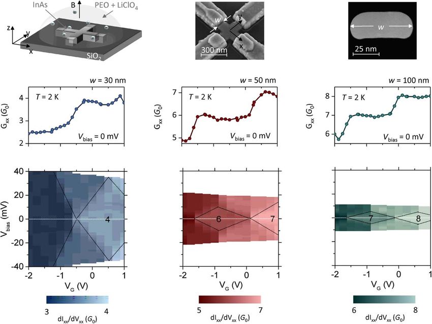
Semicond. Sci. Technol. 34 (2019) 035028 J Gooth et al
Figure 1. One-dimensional quantized conductance at zero magnetic field. (a) Scheme of the electrical transport device. All four terminals are
contacted. An electrolyte gate (PEO+LiClO4) is used to tune the Fermi level of the device. Optionally, a magnetic field B can be applied.
(b) Scanning electron beam micrograph of a cross-junction. The InAs channel width w is the same for all terminals. (c) Zero-bias
(Vbias=0 mV) line cuts of the differential longitudinal conductance Gxx=dI/dVbias of a 30 nm-wide, (d) a 50 nm-wide and (e) a 100 nm-
wide NW channel. (f) Gxx-(Vgate, Vbias) colour plots of a 30 nm-wide, (g) a 50 nm-wide and (h) a 100 nm-wide NW channel. The numbers
denote the index of the individual sub-band.
longitudinal resistance of the InAs cross-junctions, contact operated at accelerating voltages of 30 and 5 kV. STEM
resistances of (6.7±0.4) kΩ were subtracted on all low imaging and STEM-energy dispersive x-ray spectroscopy
temperature data shown [35, 39]. NW cross-junctions (EDX) analysis are performed using a double spherical
(figure 1(b)) with widths (w=30, 50 and 100 nm) and a height aberration-corrected microscope (JEOL JEM-ARM200F),
(h=25 nm) in the range of the Fermi wavelength λ of InAs operated at 200 kV, and equipped with a silicon drift detector
(typically λInas ≈ 35 nm) [27] are investigated. Hall measure- (JEOL Dry SD100GV) with 100 mm2 detection area for EDX
ments on our devices at 300 K (supplemental material (SM) is analysis.
available online at stacks.iop.org/SST/34/035028/mmedia)
reveal an electron concentration of about 5 ´ 1017cm-3 and a
mobility between 3700 and 6000 cm2 V−1 s−1, decreasing with Results and discussion
shrinking width, which we attribute to increased surface scat-
tering. We note that all obtained results are independent of One-dimensional quantized conductance at zero magnetic
contact terminal iteration (see SM for details). field
In a first transport experiment, we verify that the InAs
Scanning transmission electron microscopy analysis
nanowire cross-junctions are ballistic 1D quantum wire sys-
For structural and compositional analysis of the NW devices, tems at zero magnetic field. Therefore, low temperature
Scanning Transmission Electron Microscopy (STEM) is (T=2 K) bias spectroscopy is performed with no magnetic
performed. Cross-sectional lamellas are prepared by means of field applied (B=0 T). Consistent with our previous studies,
an FEI Helios Nanolab 450 S focused ion beam instrument [35, 39] the NW cross-junctions exhibit plateaus at integer
3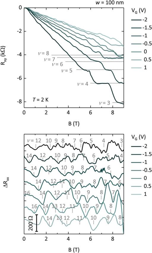
Semicond. Sci. Technol. 34 (2019) 035028 J Gooth et al
multiples n of 2e2/h shown in the zero-bias (Vbias=0 mV) onset of transport in an additional sub-band, the maxima of g
line cuts of the differential longitudinal conductance Gxx= can be associated with the sub-band energies. For all inves-
dI/dVbias (figures 1(c)–(e))-the hallmark of ballistic 1D tigated NW samples, the sub-bands are indexed with n,
quantum transport [17, 18, 22]. As expected from the simple starting from the zero-field plateau values. n scales non-linear
model of an infinite 1D quantum well, the energy level spa- with inverse magnetic field, consistent with a continuous
cing DEi, j, given by the tips of the diamond-like structures in depopulation of the 1D states. Zeeman splitting of the sub-
the 2D Gxx-(Vgate, Vbias) colour plots of figures 1(f)–(h), bands is reflected by branching of the individual maximum-
resembles the 1D sub-band splitting of the previously inves- traces at high magnetic field as indicated by arrows (spin up
tigated single InAs NWs [35] and InAs NW cross-junctions and spin down) [20–22]. In addition, plotting the filling factor
[39]. Also, consistently, the smaller the NW channel width, ν=2n into fan diagrams (figures 2(g)–(i)), provides finger-
the larger the size quantization and thus the gapping of the 1D prints of a transition from size quantization at zero B-field to
sub-bands (w=30 nm: ΔE3,4=35 meV; w=50 nm: Landau quantization in high fields as indicated by the grey
ΔE5,6=12 meV; w=50 nm: ΔE6,7=8 meV). We note dotted lines: [44, 46] Being non-linear at high 1/B-values
that despite the similar carrier concentrations for zero gate (low magnetic fields), the index-plots exhibit a linear relation
voltage at 300 K, the sub-band population at 2 K depends on between ν and 1/B at low 1/B-values (high fields), tracing the
the NW channel width. This is, because the thermal activation theoretical description of Shubnikov-de Haas oscillations.
energy becomes smaller than the size of the sub-band spacing The emergence of this linear relation is expected in the limit,
and thus the point in VG where transport through the 1D states heB
where the Landau level splitting DEB = greatly
commences is linked to the strength of the size quantization at 2pm*
low temperatures. In comparison to previously investigated exceeds the 1D sub band spacing DEi, j [44, 46]. Employing
back-gated devices, no full pinch-off is reached in any device, the effective mass of bulk InAs m*=0.023m0, we find the
because the 20 nm-thick template oxide weakens the effect of centres of the 1D–2D transition (DEB = DEi, j ) at around
the liquid ion gate. B=7 T, 4 T and 1.2 T for the 30 nm-wide, the 50 nm-wide
and the 100 nm-wide NW channels, respectively. These
results agree reasonable well with a size-dependent, smooth
One-dimensional sub-band depopulation in low magnetic field crossover from 1D conductance quantization to hybrid mag-
Next, we investigate the evolution of the 1D features within a netoelectric sub-bands in our InAs NW cross-junction data,
magnetic field. When applying a magnetic field B perpend- eventually transforming into edge states for the 100 nm-wide
icular to the plane of the cross-junction, we observe a step- devices in high B [47].
wise increase of Rxx(B) in multiples of G–1 0 at low B
(figures 2(a)–(c)). This is a signature of Landau quantization
Quantum hall regime at high magnetic field
and corresponds to the magnetic depopulation of the 1D sub-
bands with increasing field [43, 44]. Compared to previous Having established the transformation from one-dimensional
studies on InSb [5, 17] and InAs [22] NWs at mK tempera- bulk states in low B to edge-channels in high B using long-
tures, where indications for Zeeman-split sub-bands of lifted itudinal transport parameters, we now turn to investigate the Hall
spin-degeneracy are observed, which is reflected by half- resistance Rxy of the NW cross-junctions. For the 30 nm-wide
integer (G0/2)−1-features between the resistance plateaus, and the 50 nm-wide NW channels, the Hall response under
such features are not obvious from our raw data. This is applied magnetic field is strongly suppressed and no significant
probably due to the finite current bias as well as the elevated voltage signal could be measured. This may be explained by the
base temperature used in our experiment. However, as shown fact that for the magnetic field range applied, the electron-tra-
later, signatures of Zeeman splitting can be obtained by fur- jectories cannot enter a side probe directly, since their cyclotron
ther data processing. At magnetic fields above 5 T, the pla- radii are larger than the widths of the side arms. In the case of the
teau-like 1D levels in the magnetoresistance of the widest 100 nm-wide device, however, we measure a Hall response
cross-junction (w=100 nm) evolve into peaks. Such trans- above 0.5 T and observe well-defined integer quantum Hall
ition in the Landau level spectrum is a first indication for a plateaus Rxy=(ve2/h)−1 for B>5 T (figure 3(a)), which
transformation of the electronic structure in these NW struc- position in B matches the position of the above the minima of
tures [45]. the longitudinal resistance data. In the extreme quantum limit,
the Rxx is expected to vanish in the quantum Hall state. Rxx in the
InAs NW system, however, remains finite, which could be
Magnetic field-dependence of the sub-bands
explained by the finite temperature and limited magnetic field
To investigate this transition in more detail, we calculate the range investigated or parallel conduction paths of surface and
derivative of the inverse longitudinal resistance with respect bulk. For clarity reasons, a smooth 2nd order polynomial
to the gate voltage g=d(1/Rxx)/dVG, which relates to the background is subtracted from Rxx to obtain ΔRxx (figure 3(b))
magnetoelectric band structure of the NW devices. The results as is usually done to distinguish the Shubnikov-de Haas oscil-
for the 30 nm-wide device is shown in figure 2(d)), for the lations on the surface of topological insulators from the bulk.
50 nm-wide device in figure 2(e) and for the 100 nm-wide The 1D sub-bands, which carry the current at zero field seem to
device in figure 2(f)) [5, 17, 22]. Because in 1D, the transition be smoothly transformed into edge channels when exposed to an
between the longitudinal resistance plateaus is linked with the out-of-plane magnetic field. Our observation is concurrent with
4Semicond. Sci. Technol. 34 (2019) 035028 J Gooth et al
Figure 2. Magnetoelectric sub-band structure. (a) Longitudinal electrical resistance Rxx(B)=Vxx(B)/Ixx at 2 K for various gate voltages VG of a
30 nm-wide, (b) a 50 nm-wide and (c) a 100 nm-wide NW channel. At low magnetic fields, the magnetoresistance scales in steps of the inverse
multiples of the conductance quantum (nG0)−1=(n2e2/h)−1. (d)–(f) Longitudinal differential inverse resistance g=d(1/Rxx)/dVG as function
of gate voltage VG and perpendicular magnetic field B for each channel width. The onset of the sub-bands is represented by the minima
and indexed with integers n. Spin-splitting at higher field is marked by arrows (spin up and down). The white dotted lines are guides to the eyes.
(g)–(h) Landau-index ν =2n fan diagrams for various gate voltages. The grey lines represent the 2D limit at high magnetic fields.
the recent interpretation of Landau level formation in InAs NW
Robustness of the quantum hall state
QPCs [21]. Further, as the B field is decreased, Rxy exhibits the
tendency of a last plateau near B=0 T (see SM for details). Finally, we investigate the robustness of the QH state in the
This is a feature of 1D confinement, [46, 48] which originates cross-junction. The edge channels are predicted to be topo-
from the fact that at small magnetic fields the Landau level logically protected and therefore expected to be immune to
splitting does not become arbitrary small, but evolves into the disorder. In a 100 nm-wide NW sample, both ballistic 1D
discrete 1D sub-band splitting. transport at zero field and the QH state at high magnetic fields
5Semicond. Sci. Technol. 34 (2019) 035028 J Gooth et al
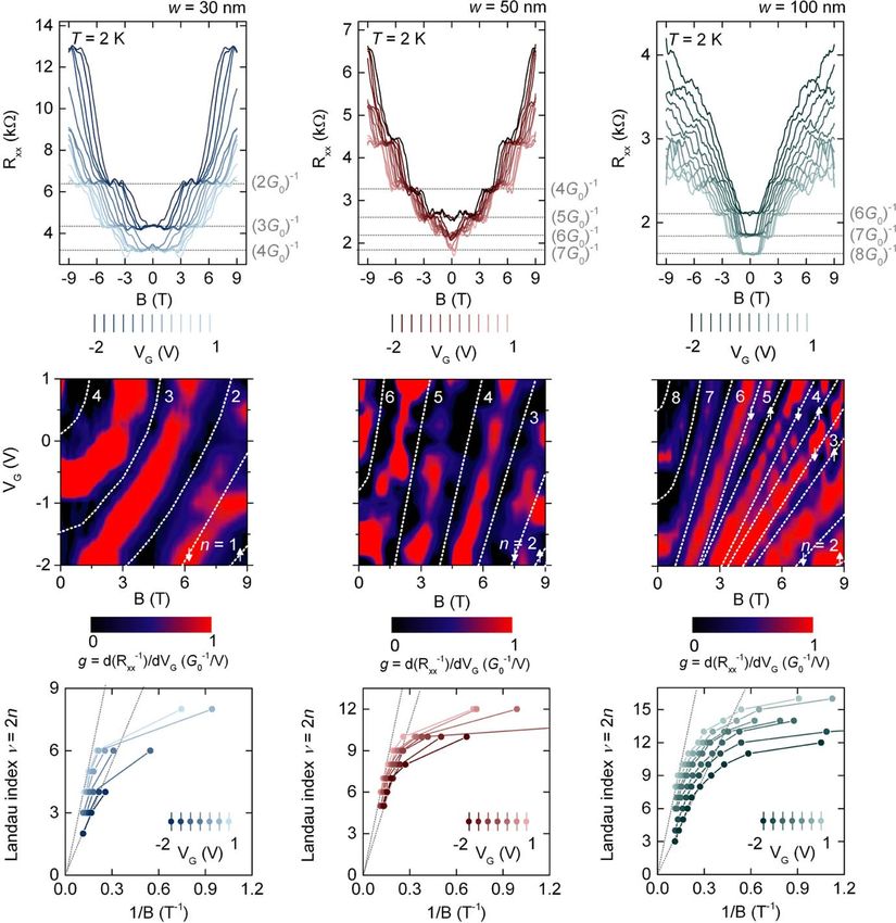
This is due to the creation of dangling bonds, trap states,
surface dipoles and surface oxides that not only induce a
morphological disorder, but also impact the electronic band
structure of the surface [49].
To address the effect of template-removal in more detail,
the surface of both types of devices was investigated by
energy dispersive x-ray (EDX) spectroscopy analysis in
STEM mode. The line-cut data, taken as indicated in
figures 4(a) and (b), reveals that compared to the protected
NW (figure 4(c)), the template-removing procedure leads to
the formation of a 6 nm-thick non-stochiometric phase at the
NW surface (figure 4(d)) that modifies the electronic prop-
erties. In magneto-transport experiments (figures (e), (f)), we
confirm that the quantized conductance steps at low magnetic
fields are clearly suppressed in cross-junction with the dis-
ordered surface. Around zero magnetic field, a resistance peak
is observed, which is a signature of weak localization [42]-a
quantum mechanical interference effect that is caused by
closed-loop elastic scattering paths. As the magnetic field is
increased, the magnetoresistance exhibits a maximum at
around Bc=1.3 T, marking the chambers field, which is
explained by surface wall scattering: [50] this arises when
bulk scattering is small and low magnetic fields force the
electrons against the sidewalls of the NW channel. Disorder at
the surface will then cause scattering and the magnetoresis-
tance increases as the magnetic field is enhanced. However,
when B is increased further, such that magnetic confinement
in the NW channel becomes smaller than the spatial con-
finement, surface scattering is reduced and the magnetore-
sistance decreases again. Consistent with this interpretation,
the determined Bc=5 T agrees well with the centre of the
transition from the 1D conductance quantization to the QH
regime in the template-protected samples. At higher magnetic
fields, the minima on the smoothly varying background
Figure 3. Hall effect in InAs nanowire cross junctions. (a) Hall
resistance Rxy=Vxy(B)/Ixx of a 100 nm-wide NW cross-junction at resemble the minima, indexed by ν in the longitudinal mag-
2 K for various gate voltages VG as a function of magnetic field B. netoresistance of the protected InAs NW cross-junction
For B>5 T, plateaus scaling with (ve2/h)−1 occur. (b) Residual (figure 4(e)). This indicates that at high B the sub-band
resistance ΔRxx for the same device at 2 K for various gate voltages structure of the as-grown NW is recovered, despite the dis-
VG as a function of magnetic field B. To obtain ΔRxx, a smooth
order at the surface. Consistently we observed that, while
polynomial background is subtracted from Rxx. The minima denote
the Landau level v, indexed by grey numbers. ballistic 1D transport in zero magnetic is fragile against dis-
order at the NW surface, the QH plateaus at high magnetic
fields remain robust. Consequently, Rxy, measured on the
are observable. By introducing random surface charges, we disordered cross-junction shows distinct plateaus, centred on
disturb the ballistic condition along the nanowire axis at zero the minima of the Rxx-B data. The height of the plateaus
magnetic field; thus, the quantized resistance plateaus of agrees well with the Hall data obtained for the protected NW
(n2e2/h)−1 should be suppressed, in contrast to the edge structure Rxy=(νe2/h)−1 for B>Bc=5 T and is therefore
channels of the QH state which are not localized, due to consistent with the Landau-level-interpretation of the max-
the topological protection, as long as the disorder does not imum in Rxx above. This concludes that the observed QH state
create inelastic scattering events. To carry out this test, we is robust against disorder, which is strong enough to supress
compare the devices protected by the SiO2 template with the transmission of 1D modes at zero magnetic field. A
devices, on which scattering is purposely induced at the similar test has recently been carried out on Bi2Se3 NWs, [51]
surface of the NW cross-junction by removing the protective demonstrating topological protection of helical surface
SiO2 template in diluted hydrofluoric acid and subsequently modes. We therefore believe that the robustness of the QH
storing the samples for 6 d in air. It is well-known that the state observed in here, is a strong signature for topologically
electronic transport properties of III–V NW surfaces are protected edge channel transport in InAs NW cross-junctions
modified when subjected to ambient conditions, [49] with the at high magnetic fields. However, we note that at high
dominant mechanism being carrier scattering at the surface. magnetic fields, the smooth background of the Rxx-B has
6Semicond. Sci. Technol. 34 (2019) 035028 J Gooth et al
Figure 4. Comparison of template-protected and air-exposed NW devices. (a) Scanning transmission micrograph of an InAs NW channel
(light grey area) within the template and (b) after removing the template. (c), (d) STEM-EDX line profiles obtained along the white dotted
lines in panels a and b. While the stoichiometry of the protected NW channel is InAs 1:1 at the NW/template interface, the NW with
removed template exhibits an indium-rich surface layer of about 6 nm. (e) Magneto-transport data at zero gate voltage and 2 K for a 100 nm-
wide NW cross-junction before and (f) after removing the template. The ballistic 1D transport is fragile against the disorder at the channel’s
surface. A weak-localization peak evolves around B=0 and Chambers peaks of boundary scattering, marked by Bc are observed when the
template is removed. At high magnetic fields, the sub-band structure and the Hall plateaus of the disordered device resemble the features
observed for the protected NW.
changed, the reason for which is not clear and requires further the edge channel transport in the QH state remained robust,
investigation. which we believe provides evidence for topological protec-
tion. Therefore, such NW quantum Hall devices can be useful
for applications in fault-tolerant quantum computing and non-
Conclusion dissipative electronic devices. However, there are still two
main obstacles to overcome: the QH state only exists at low
In conclusion, we have implemented ballistic 1D NWs with temperatures and high magnetic fields. Following the exam-
well-controlled cross-section into a crossbar geometry and ple of the quantum spin Hall effect in 2D quantum wells,
provided the first demonstration of a protected QH state in [52, 53] topologically protected edge channel transport
these systems. Magneto-transport experiments reveal that the without magnetic field might also be obtainable in future 1D
ballistic 1D quantum system at zero field smoothly evolves NW devices.
into the QH regime in perpendicular magnetic fields. Careful
material design, enabled by the TASE process, was critical to
study this transition. As expected from theory, [45] the Acknowledgments
transition from 1D to the QH regime occurs around the same
B-field (Bc=5 T), where the magnetic confinement over- The authors acknowledge W Hansen for fruitful discussions.
comes the spatial size confinement. The template-protected We thank M Tschudy for metallization of the devices and
devices enabled an exploration of ballistic 1D transport and technical support. The research leading to these results has
test its stability upon inducing disorder at the NW surface. received funding from the European Union’s Horizon 2020
While the ballistic transmission of 1D modes was supressed, research and innovation program under grant agreement No
7Semicond. Sci. Technol. 34 (2019) 035028 J Gooth et al
687931 ‘REMINDER’, the European Union Seventh Frame- References
work Programs (FP7/2007–2013), No. 619509 ‘E2SWITCH’,
the Marie Curie Post-Doctoral Research Fellowship No. [1] Ferry D K 2008 Nanowires in nanoelectronics Science 319 579
704045 ‘MODES’, and, also the Rudolf Diesel Industry Fel- [2] Heedt S, Vakulov D, Rieger T, Rosenbach D, Trellenkamp S,
lowship funded by the EU Marie Curie Cofund Program (FP7- Grützmacher D, Lepsa M I and Schäpers T 2016 Electronic
MC-COFUND, grant agreement No. 291763), and also the properties of complex self-assembled InAs nanowire
networks Adv. Electron. Mater. 2 1500460
Swiss National Science Foundation (SNSF) with project no.
[3] Gooth J, Borg M, Schmid H, Schaller V, Wirths S,
200021_156746. Moselund K, Luisier M, Karg S and Riel H 2017 Ballistic
one-dimensional InAs nanowire cross-junction interconnects
Nano Lett. 17 2596–602
Associated content [4] Plissard S R et al 2013 Formation and electronic properties of
InSb nanocrosses Nat. Nanotechnol. 8 859–64
[5] Fadaly E M T, Zhang H, Conesa-Boj S, Car D, Gül Ö,
The supporting material includes Hall measurements of all Plissard S R, Op het Veld R L M, Kölling S,
devices at 300 K, the magneto-transport data of the 100 nm- Kouwenhoven L P and Bakkers E P A M 2017 Observation
wide device at 2 K and zero gate voltage with iterated term- of conductance quantization in InSb nanowire networks
inals as well as a zoom-in to the suppressed Hall resistance Nano Lett. 17 6511–5
[6] Das A, Ronen Y, Most Y, Oreg Y, Heiblum M and
around zero magnetic field and Hall traces of all devices
Shtrikman H 2012 Zero-bias peaks and splitting in an Al-
investigated at 2 K. InAs nanowire topological superconductor as a signature of
majorana fermions Nat. Phys. 8 887–95
[7] Mourik V, Zuo K, Frolov S M, Plissard S R,
Author contributions Bakkers E P a. M and Kouwenhoven L P 2012 Signatures of
majorana fermions in hybrid superconductor-semiconductor
nanowire devices Science 336 1003–7
JG and MB conceived the original idea for the study. MB, HS
[8] del Alamo J A 2011 Nanometre-scale electronics with III–V
and SW synthesized the InAs nanowires. MB and JG fabri- compound semiconductors Nature 479 317–23
cated the NW devices. JG carried out the transport mea- [9] Riel H, Wernersson L-E, Hong M and del Alamo J A 2014 III–
surements. NB and MR. carried out the STEM-EDX analysis. V compound semiconductor transistors—from planar to
JG MB. and HS analyzed the data. HR, KM and KN super- nanowire structures MRS Bull. 39 668–77
[10] Dayeh S A, Aplin D P R, Zhou X, Yu P K L, Yu E T and
vised the project. All authors contributed to the interpretation
Wang D 2007 High electron mobility InAs nanowire field-
of the data and to the writing of the manuscript. effect transistors Small 3 326–32
[11] Burke A M, Carrad D J, Gluschke J G, Storm K,
Fahlvik Svensson S, Linke H, Samuelson L and
Funding sources Micolich A P 2015 InAs nanowire transistors with multiple,
independent wrap-gate segments Nano Lett. 15 2836–43
[12] Storm K, Nylund G, Samuelson L and Micolich A P 2012
European Union’s Horizon 2020 research and innovation Realizing lateral wrap-gated nanowire FETs: controlling gate
program under grant agreement No 687931 ‘REMINDER’, length with chemistry rather than lithography Nano Lett. 12 1–6
the European Union Seventh Framework Programs (FP7/ [13] Carrad D J, Burke A M, Lyttleton R W, Joyce H J, Tan H H,
2007–2013), No. 619509 ‘E2SWITCH’, the Marie Curie Jagadish C, Storm K, Linke H, Samuelson L and
Micolich A P 2014 Electron-beam patterning of polymer
Post-Doctoral Research Fellowship No. 704045 ‘MODES’,
electrolyte films to make multiple nanoscale gates for
and, also the Rudolf Diesel Industry Fellowship funded by the nanowire transistors Nano Lett. 14 94–100
EU Marie Curie Cofund Program (FP7-MC-COFUND, grant [14] Lind E, Persson A I, Samuelson L and Wernersson L E 2006
agreement No. 291763). Improved subthreshold slope in an InAs nanowire
heterostructure field-effect transistor Nano Lett. 6 1842–6
[15] Tian Y, Sakr M R, Kinder J M, Liang D, MacDonald M J,
Qiu R L J, Gao H J and Gao X P A 2012 One-dimensional
Competing interests
quantum confinement effect modulated thermoelectric
properties in InAs nanowires Nano Lett. 12 6492–7
The authors declare no competing interests. [16] Gooth J, Schaller V, Wirths S, Schmid H, Borg M, Bologna N,
Karg S and Riel H 2017 Ballistic one-dimensional transport
in InAs nanowires monolithically integrated on silicon Appl.
Data availability Phys. Lett. 110 083105
[17] Van Weperen I, Plissard S R, Bakkers E P A M,
Frolov S M and Kouwenhoven L P 2013 Quantized
All data generated or analyzed during this study are included in conductance in an InSb nanowire Nano Lett. 13 387–91
this published article (and its Supplementary Material files). [18] Kammhuber J et al 2016 Conductance quantization at zero
magnetic field in InSb nanowires Nano Lett. 16 3482–6
[19] Abay S, Persson D, Nilsson H, Xu H Q, Fogelström M,
ORCID iDs Shumeiko V and Delsing P 2013 Quantized conductance
and its correlation to the supercurrent in a nanowire
connected to superconductorS Nano Lett. 13 3614–7
Johannes Gooth https://orcid.org/0000-0002-4062-3232 [20] Heedt S, Traverso Ziani N, Crépin F, Prost W, Trellenkamp S,
Mattias Borg https://orcid.org/0000-0003-1217-369X Schubert J, Grützmacher D, Trauzettel B and Schäpers T
8Semicond. Sci. Technol. 34 (2019) 035028 J Gooth et al
2017 Signatures of interaction-induced helical gaps in measurements on InAs nanowires Appl. Phys. Lett. 101
nanowire quantum point contacts Nat. Phys. 13 563–7 152106–10
[21] Heedt S, Manolescu A, Nemnes G A, Prost W, Schubert J, [37] Storm K, Halvardsson F, Heurlin M, Lindgren D,
Grützmacher D and Schäpers T 2016 Adiabatic edge Gustafsson A, Wu P M, Monemar B and Samuelson L 2012
channel transport in a nanowire quantum point contact Spatially resolved hall effect measurement in a single
register Nano Lett. 16 4569–75 semiconductor nanowire Nat. Nanotechnol. 7 718–22
[22] Heedt S, Prost W, Schubert J, Grützmacher D and Schäpers T [38] Hultin O, Otnes G, Borgström M T, Björk M, Samuelson L and
2016 Ballistic transport and exchange interaction in InAs Storm K 2016 Comparing hall effect and field effect
nanowire quantum point contacts Nano Lett. 16 3116–23 measurements on the same single nanowire Nano Lett. 16
[23] Zota C B, Lindgren D, Wernersson L-E and Lind E 2015 205–11
Quantized conduction and high mobility in selectively [39] Gooth J, Borg M, Schmid H, Schaller V, Wirths S,
grown InxGa1–xAs nanowires ACS Nano 9 9892–7 Moselund K, Luisier M, Karg S and Riel H 2017 Ballistic
[24] Björk M T, Fuhrer A, Hansen A E, Larsson M W, one-dimensional InAs nanowire cross-junction interconnects
Fröberg L E and Samuelson L 2005 Tunable effective g Nano Lett. 17 2596–602
factor in InAs nanowire quantum dots Phys. Rev. B 72 [40] Schmid H, Borg M, Moselund K, Gignac L, Breslin C M,
201307 Bruley J, Cutaia D and Riel H 2015 Template-assisted selective
[25] Wallin D, Fuhrer A, Fröberg L E, Samuelson L, Xu H Q, epitaxy of III–V nanoscale devices for co-planar heterogeneous
Hofling S and Forchel A 2007 Detection of charge states in integration with Si Appl. Phys. Lett. 106 233101
nanowire quantum dots using a quantum point contact Appl. [41] Borg M, Schmid H, Moselund K E, Cutaia D and Riel H 2015
Phys. Lett. 90 172112 Mechanisms of template-assisted selective epitaxy of InAs
[26] Fasth C, Fuhrer A, Samuelson L, Golovach V N and Loss D nanowires on Si J. Appl. Phys. 117 144303–9
2007 Direct measurement of the spin-orbit interaction in a [42] Liang D and Gao X P A 2012 Strong tuning of rashba spin-
two-electron InAs nanowire quantum dot Phys. Rev. Lett. 98 orbit interaction in single InAs nanowires Nano Lett. 12
266801–4 3263–7
[27] Wu P M, Gooth J, Zianni X, Svensson S F, Gluschke J G, [43] Van Wees B J, Kouwenhoven L P, Van Houten H,
Dick K a, Thelander C, Nielsch K and Linke H 2013 Large Beenakker C W J, Mooij J E, Foxon C T and Harris J J 1988
thermoelectric power factor enhancement observed in InAs Quantized conductance of magnetoelectric subbands in
nanowires Nano Lett. 13 4080–6 ballistic point contacts Phys. Rev. B 38 3625–7
[28] Blömers C, Lepsa M I, Luysberg M, Grtzmacher D, [44] Tso H C and Vasilopoulos P 1991 Magnetotransport along a
Lüth H and Schäpers T 2011 Electronic phase coherence in quantum wire Phys. Rev. B 44 12952–8
InAs nanowires Nano Lett. 11 3550–6 [45] Chu D P and Butcher P N 1993 Intrinsic integer quantum Hall
[29] Vigneau F, Prudkovkiy V, Duchemin I, Escoffier W, Caroff P, effect in a quantum wire Phys. Rev. B 47 10008–11
Niquet Y-M, Leturcq R, Goiran M and Raquet B 2014 [46] Roukes M L, Scherer A, Allen S J, Craighead H G,
Magnetotransport subband spectroscopy in InAs nanowires Ruthen R M, Beebe E D and Harbison J P 1987 Quenching
Phys. Rev. Lett. 112 76801 of the hall effect in a one-dimensional wire Phys. Rev. Lett.
[30] Dhara S, Solanki H S, Singh V, Narayanan A, Chaudhari P, 59 3011–4
Gokhale M, Bhattacharya A and Deshmukh M M 2009 [47] Ando T 1990 Edge states in quantum wires in high magnetic
Magnetotransport properties of individual InAs nanowires fields Phys. Rev. B 42 5626–34
Phys. Rev. B 79 121311 [48] Beenakker C W J and Van Houten H 1988 Quenching of the
[31] Liang D and Gao X P A 2012 Strong tuning of rashba spin- hall effect Phys. Rev. Lett. 60 2406–9
orbit interaction in single InAs nanowires Nano Lett. 12 [49] Thathachary A V, Agrawal N, Liu L and Datta S 2014 Electron
3263–7 transport in multigate InxGa1-x as nanowire FETs: from
[32] Roulleau P, Choi T, Riedi S, Heinzel T, Shorubalko I, diffusive to ballistic regimes at room temperature Nano Lett.
Ihn T and Ensslin K 2010 Suppression of weak 14 626–33
antilocalization in InAs nanowires Phys. Rev. B 81 155449 [50] Thornton T J, Roukes M L, Scherer A and Van De Gaag B P
[33] Liang D, Sakr M R and Gao X P A 2009 One-dimensional 1989 Boundary scattering in quantum wires Phys. Rev. Lett.
weak localization of electrons in a single InAs nanowire 63 2128–31
Nano Lett. 9 1709–12 [51] Hong S S, Zhang Y, Cha J J, Qi X L and Cui Y 2014 One-
[34] Sch T and Gr P 2016 Ballistic transport and exchange dimensional helical transport in topological insulator
interaction in InAs nanowire quantum point contacts Nano nanowire interferometers Nano Lett. 14 2815–21
Lett. 16 3116–163123 [52] Bernevig B A, Hughes T L and Zhang S-C 2006 Quantum spin
[35] Gooth J, Schaller V, Wirths S, Schmid H, Borg M, Bologna N, hall effect and topological phase transition in HgTe quantum
Karg S and Riel H 2017 Ballistic one-dimensional transport wells Science 314 1757–61
in InAs nanowires monolithically integrated on silicon Appl. [53] König M, Wiedmann S, Brüne C, Roth A, Buhmann H,
Phys. Lett. 110 83105 Molenkamp L W, Qi X-L and Zhang S-C 2007 Quantum
[36] Blömers C, Grap T, Lepsa M I, Moers J, Trellenkamp S, spin hall insulator state in HgTe quantum wells Science 318
Grützmacher D, Lüth H and Schäpers T 2012 Hall effect 766–70
9You can also read