UM11178 RDGD3100I3PH5EVB three-phase inverter reference design Rev. 1 - 28 May 2019
←
→
Page content transcription
If your browser does not render page correctly, please read the page content below
UM11178
                               RDGD3100I3PH5EVB three-phase inverter reference design
                               Rev. 1 — 28 May 2019                                                                        User manual

Figure 1. RDGD3100I3PH5EVB

Important Notice
NXP provides the enclosed product(s) under the following conditions:
This reference design is intended for use of ENGINEERING DEVELOPMENT OR EVALUATION PURPOSES ONLY. It is provided as a
sample IC pre-soldered to a printed circuit board to make it easier to access inputs, outputs, and supply terminals. This reference design
may be used with any development system or other source of I/O signals by simply connecting it to the host MCU or computer board via
off-the-shelf cables. Final device in an application will be heavily dependent on proper printed circuit board layout and heat sinking design
as well as attention to supply filtering, transient suppression, and I/O signal quality.
The goods provided may not be complete in terms of required design, marketing, and or manufacturing related protective considerations,
including product safety measures typically found in the end product incorporating the goods. Due to the open construction of the product,
it is the user's responsibility to take any and all appropriate precautions with regard to electrostatic discharge. In order to minimize risks
associated with the customers applications, adequate design and operating safeguards must be provided by the customer to minimize
inherent or procedural hazards. For any safety concerns, contact NXP sales and technical support services.
Should this reference design not meet the specifications indicated in the kit, it may be returned within 30 days from the date of delivery and
will be replaced by a new kit.
NXP reserves the right to make changes without further notice to any products herein. NXP makes no warranty, representation or
guarantee regarding the suitability of its products for any particular purpose, nor does NXP assume any liability arising out of the
application or use of any product or circuit, and specifically disclaims any and all liability, including without limitation consequential or
incidental damages. Typical parameters can and do vary in different applications and actual performance may vary over time. All operating
parameters, including Typical, must be validated for each customer application by customer’s technical experts.
NXP does not convey any license under its patent rights nor the rights of others. NXP products are not designed, intended, or authorized
for use as components in systems intended for surgical implant into the body, or other applications intended to support or sustain life, or
for any other application in which the failure of the NXP product could create a situation where personal injury or death may occur.
Should the Buyer purchase or use NXP products for any such unintended or unauthorized application, the Buyer shall indemnify and hold
NXP and its officers, employees, subsidiaries, affiliates, and distributors harmless against all claims, costs, damages, and expenses, and
reasonable attorney fees arising out of, directly or indirectly, any claim of personal injury or death associated with such unintended or
unauthorized use, even if such claim alleges NXP was negligent regarding the design or manufacture of the part.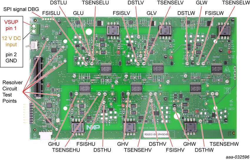
NXP Semiconductors
                                                                                                                 UM11178
                                                         RDGD3100I3PH5EVB three-phase inverter reference design

1         Introduction
                     This document is the user guide for the RDGD3100I3PH5EVB reference design.
                     This document is intended for the engineers involved in the evaluation, design,
                     implementation, and validation of single-channel gate driver for IGBT, GD3100.
                     The scope of this document is to provide the user with information to evaluate the single
                     channel gate driver for IGBT, GD3100. This document covers connecting the hardware,
                     installing the software and tools, configuring the environment and using the kit.
                     The RDGD3100I3PH5EVB is a fully functional three-phase inverter evaluation board
                     populated with six GD3100 gate drivers with fault management and supporting
                     circuitry. This board supports SPI daisy chain communication for programming and
                     communication with three high-side gate drivers and three low-side gate drivers
                     independently.
                     This board has low-voltage and high-voltage isolation in conjunction with gate drive
                     integrated galvanic signal isolation. Other supporting features on the board include
                     desaturation short-circuit detection, IGBT temperature sensing, DC Link bus voltage
                     monitoring, phase current sensing, and motor resolver excitation and signal processing
                     connection circuitry. See GD3100 data sheet for additional gate drive features.

2         Finding kit resources and information on the NXP web site
                     The NXP analog product development boards provide an easy-to-use platform for
                     evaluating NXP products. The boards support a range of analog, mixed-signal and
                     power solutions. They incorporate monolithic integrated circuits and system-in-package
                     devices that use proven high-volume technology. NXP products offer longer battery life, a
                     smaller form factor, reduced component counts, lower cost and improved performance in
                     powering state-of-the-art systems.
                     NXP Semiconductors provides online resources for this reference design and its
                     supported device(s) on http://www.nxp.com.
                     The information page for RDGD3100I3PH5EVB reference design is at http://
                     www.nxp.com/RDGD3100I3PH5EVB. The information page provides overview
                     information, specifications, ordering information, documentation and software. The
                     Documents and Software tab provides quick-reference information applicable to
                     using the RDGD3100I3PH5EVB reference design, including the downloadable assets
                     referenced in this document.

                 2.1 Collaborate in the NXP community
                     The NXP community is for sharing ideas and tips, ask and answer technical questions,
                     and receive input on just about any embedded design topic.
                     The NXP community is at http://community.nxp.com.

3         Getting started
                     Working with the RDGD3100I3PH5EVB requires the kit contents, additional hardware,
                     and a Windows PC workstation with installed software.

UM11178                             All information provided in this document is subject to legal disclaimers.   © NXP B.V. 2019. All rights reserved.

User manual                                          Rev. 1 — 28 May 2019
                                                                                                                                             2 / 18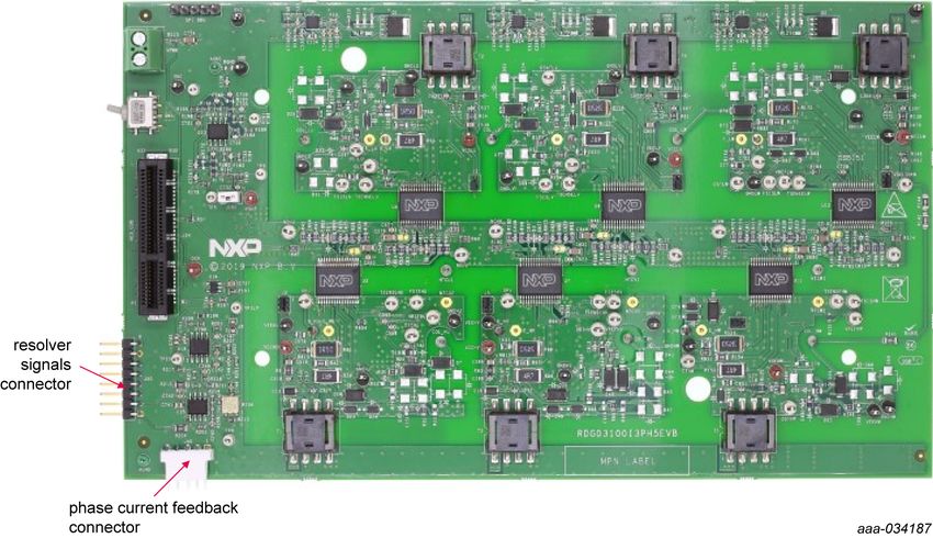
NXP Semiconductors
                                                                                                                   UM11178
                                                           RDGD3100I3PH5EVB three-phase inverter reference design

                 3.1 Kit contents
                     • Assembled and tested RDGD3100I3PH5EVB (three-phase inverter populated with
                       5.0 V compatible gate driver devices) board in an anti-static bag
                     • One PCIe cable (X-S32SDEV-CON18) for connection to MCU board (MPC5777C-
                       DEVB or MPC5744P)
                     • Quick Start Guide

                 3.2 Additional hardware
                     In addition to the kit contents, the following hardware is necessary or beneficial when
                     working with this kit.
                     •   Microcontroller for SPI communication
                     •   IGBT module Infineon HP Drive
                     •   DC link capacitor compatible with IGBT part FS820R08A6P2B
                     •   HV power supply with protection shield and hearing protection
                     •   Current sensors for monitoring each phase current
                     •   12 V, 1.0 A DC power supply
                     •   TEK MSO 4054 500 MHz 2.5 GS/s 4-channel oscilloscope

                 3.3 Windows PC workstation
                     This reference design requires a Windows PC workstation. Meeting these minimum
                     specifications should produce great results when working with this evaluation board.
                     • USB-enabled computer with Windows 7 or Windows 10

                 3.4 Software
                     Installing software is necessary to work with this reference design. All listed software
                     is available on the reference design's information page at http://www.nxp.com/
                     RDGD3100I3PH5EVB.
                     •   S32S Design Studio IDE for power architecture
                     •   Automotive Math and Motor Control Library (AMMCL)
                     •   FreeMaster 2.0 runtime debugging tool
                     •   Motor Control Application Tuning (MCAT)
                     •   Example code, GD3100 Device Driver notes and GD3100 Device Driver Reference
                         notes

4         Getting to know the hardware

                 4.1 Kit overview

               4.1.1 RDGD3100I3PH5EVB features
                     • Capability to connect to HP Drive IGBT modules for full three-phase evaluation and
                       development
                     • Daisy chain SPI communication (three high-side and three low-side gate drivers)
                     • Power supply which is jumper configurable for VEE negative or GND reference
                     • Easy access power, ground, and signal test points
UM11178                               All information provided in this document is subject to legal disclaimers.   © NXP B.V. 2019. All rights reserved.

User manual                                            Rev. 1 — 28 May 2019
                                                                                                                                               3 / 18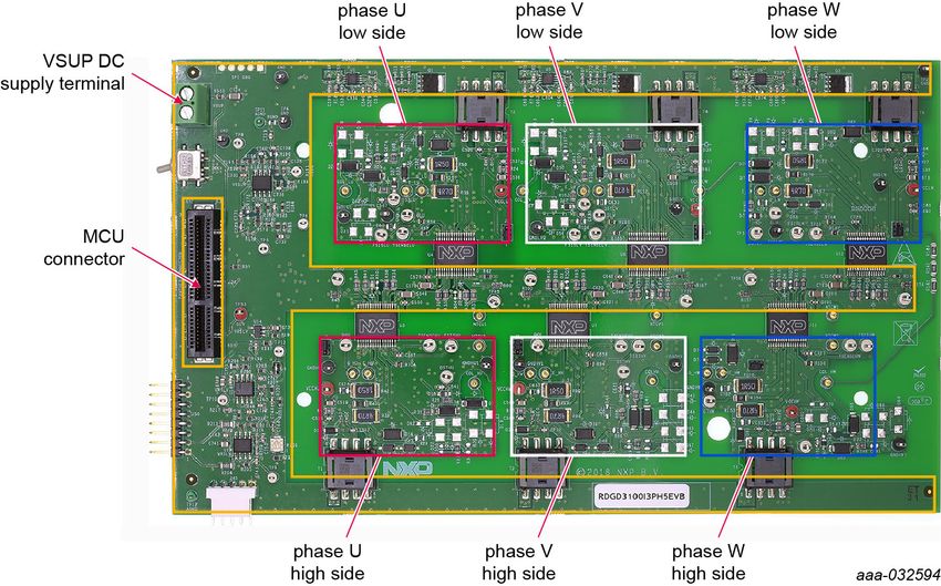
NXP Semiconductors
                                                                                                                   UM11178
                                                           RDGD3100I3PH5EVB three-phase inverter reference design

                      • 2×32 PCIe socket for interfacing MCU control
                      • Optional connection for DC bus voltage monitoring
                      • Compatible with MPC5777C-DEVB

               4.1.2 Voltage domains, GD3100 pinout, logic header, and IGBT pinout
                      Low-voltage domain is an externally supplied 12 V DC (VSUP) primary supply for non-
                      isolated circuits, typically supplied by vehicle battery. The low-voltage domain includes
                      the interface between the MCU and GD3100 control registers and logic control.
                      Low-side driver and high-side driver domains are isolated high-voltage driver control
                      domains for IGBT single phase connections and control circuits. Pins on bottom of board
                      are designed to easily connect to three-phase IGBT module.

                      Figure 2. RDGD3100I3PH5EVB three-phase inverter board voltage domains and interfaces

                4.2 Featured components

               4.2.1 Advanced IGBT gate driver

              4.2.1.1 General description

                      The GD3100 is an advanced single channel gate driver for IGBTs. Integrated Galvanic
                      isolation and low on-resistance drive transistors provide high charging and discharging
                      current, low dynamic saturation voltage, and rail-to-rail gate voltage control.
                      Current and temperature sense minimizes IGBT stress during faults. Accurate and
                      configurable under voltage lockout (UVLO) provides protection while ensuring sufficient
                      gate drive voltage headroom.
                      The GD3100 autonomously manages severe faults and reports faults and status via
                      INTB pin and a SPI interface. It is capable of directly driving gates of most IGBTs. Self-
                      test, control, and protection functions are included for design of high reliability systems
                      (ASIL C/D). It meets the stringent requirements of automotive applications and is fully
                      AEC-Q100 grade 1 qualified.

UM11178                               All information provided in this document is subject to legal disclaimers.   © NXP B.V. 2019. All rights reserved.

User manual                                            Rev. 1 — 28 May 2019
                                                                                                                                               4 / 18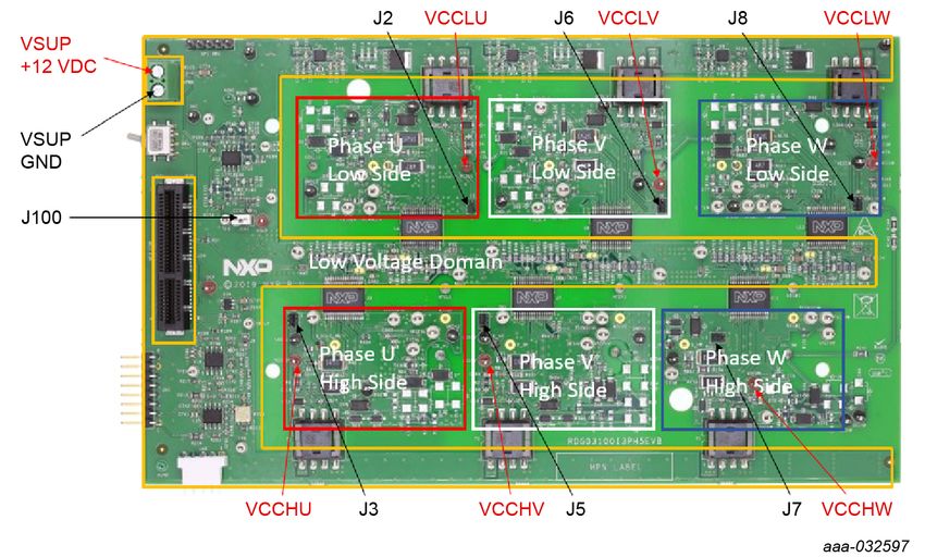
NXP Semiconductors
                                                                                                                   UM11178
                                                           RDGD3100I3PH5EVB three-phase inverter reference design

              4.2.1.2 GD3100 features

                     •   Compatible with current sense and temp sense IGBTs
                     •   Fast short-circuit protection for IGBTs with current sense feedback
                     •   Compliant with ASIL D ISO 26262 functional safety requirements
                     •   SPI interface for safety monitoring, programmability, and flexibility
                     •   Integrated Galvanic signal isolation
                     •   Integrated gate drive power stage capable of 10 A peak source and sink
                     •   Interrupt pin for fast response to faults
                     •   Compatible with negative gate supply
                     •   Compatible with 200 V to 1700 V IGBTs, power range > 125 kW
                     •   AEC-Q100 grade 1 qualified

               4.2.2 GD3100 pinout and MCU interface pinout
                     See GD3100 advanced IGBT gate driver data sheet for specific information about pinout,
                     pin descriptions, specifications, and operating modes.
                     VSUP DC supply terminal is a low voltage input connection for supplying power to the
                     low voltage non-isolated die and related circuitry. Typically supplied by vehicle battery
                     +12 V DC.
                     MCU connector is a 2×32-pin PCIe interface connector for use with either MPC5744P or
                     MPC5777C 32-bit MCU board or any other MCU of preference. An MCU is needed for
                     SPI communication and control of advanced IGBT gate drive devices (GD3100).

UM11178                               All information provided in this document is subject to legal disclaimers.   © NXP B.V. 2019. All rights reserved.

User manual                                            Rev. 1 — 28 May 2019
                                                                                                                                               5 / 18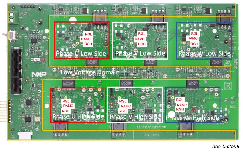
NXP Semiconductors
                                                                                                                          UM11178
                                                  RDGD3100I3PH5EVB three-phase inverter reference design

               Figure 3. Gate driver pinout and board interface connection PCIe 2×32

              Table 1. PCIe connector pin definitions
               Pin                  Name                                             Function
               A1                   VDDA                                             Voltage reference resolver circuit
               A2                   GNDA1                                            Analog ground
               A3                   PH_U_I                                           Current feedback phase U
               A4                   PH_V_I                                           Current feedback phase V
               A5                   PH_W_I                                           Current feedback phase W
               A6                   n.c.                                             not connected
               A7                   n.c.                                             not connected
               A8                   SIN_OUT_RSLV                                     Sine resolver signal
               A9                   COS_OUT_RSLV                                     Cosine resolver signal
               A10                  n.c.                                             not connected
               A11                  GNDA4                                            Analog ground
               A12                  n.c.                                             not connected
               A13                  GND2                                             Ground
               A14                  PWMHU                                            Pulse width modulation high-side phase U
               A15                  PWMLU                                            Pulse width modulation low-side phase U

UM11178                      All information provided in this document is subject to legal disclaimers.                   © NXP B.V. 2019. All rights reserved.

User manual                                   Rev. 1 — 28 May 2019
                                                                                                                                                      6 / 18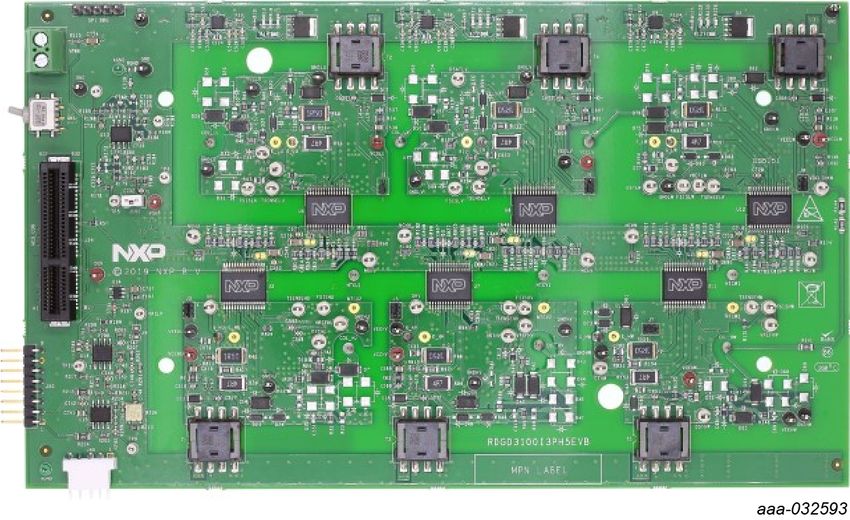
NXP Semiconductors
                                                                                                               UM11178
                                          RDGD3100I3PH5EVB three-phase inverter reference design

               Pin          Name                                             Function
               A16          PWMHV                                            Pulse width modulation high-side phase V
               A17          PWMLV                                            Pulse width modulation low-side phase V
               A18          PWMHW                                            Pulse width modulation high-side phase W
               A19          PWMLW                                            Pulse width modulation low-side phase W
               A20          n.c.                                             not connected
               A21          n.c.                                             not connected
               A22          AOUTHW                                           Analog output signal high-side phase W
               A23          n.c.                                             not connected
               A24          n.c.                                             not connected
               A25          n.c.                                             not connected
               A26          INTBHU                                           GD3100 fault reporting pin for high-side phase U
               A27          INTBLU                                           GD3100 fault reporting pin for low-side phase U
               A28          INTBHV                                           GD3100 fault reporting pin for high-side phase V
               A29          INTBLV                                           GD3100 fault reporting pin for low-side phase V
               A30          CSBH                                             Chip select bar to high gate drive devices
               A31          INTBHW                                           GD3100 fault reporting pin for high-side phase W
               A32          INTBLW                                           GD3100 fault reporting pin for low-side phase W
               B1           VREF                                             Voltage reference from MCU
               B2           GNDA2                                            Analog ground
               B3           NC                                               not connected
               B4           DCV                                              Optional DC bus voltage monitoring (not used by default)
               B5           n.c.                                             not connected
               B6           n.c.                                             not connected
               B7           n.c.                                             not connected
               B8           SIN_N_OUT_RSLV                                   Sine resolver signal
               B9           COS_N_OUT_RSLV                                   Cosine resolver signal
               B10          n.c.                                             not connected
               B11          GNDA3                                            Analog ground
               B12          MCU_VCC                                          MCU VCC regulator voltage
               B13          GND1                                             Ground
               B14          AOUTHU                                           GD3100 analog output signal high-side U phase
               B15          AOUTLU                                           GD3100 analog output signal low-side U phase
               B16          AOUTLV                                           GD3100 analog output signal low-side V phase
               B17          AOUTHV                                           GD3100 analog output signal high-side V phase
               B18          AOUTLW                                           GD3100 analog output signal low-side W phase
               B19          RES_REF                                          Resolver reference voltage
               B20          SW_RUN                                           Signal from onboard switch demo mode
               B21          MISO_MICRO                                       SPI slave out signal
               B22          MOSI_MICRO                                       SPI slave in signal
               B23          SCLK                                             SPI clock
               B24          CSBL                                             Chip select bar to low-side gate drivers

UM11178              All information provided in this document is subject to legal disclaimers.                 © NXP B.V. 2019. All rights reserved.

User manual                           Rev. 1 — 28 May 2019
                                                                                                                                            7 / 18
NXP Semiconductors
                                                                                                                              UM11178
                                                           RDGD3100I3PH5EVB three-phase inverter reference design

                    Pin                      Name                                             Function
                    B25                      n.c.                                             not connected
                    B26                      n.c.                                             not connected
                    B27                      n.c.                                             not connected
                    B28                      FSENB                                            Fail-safe state enable bar
                    B29                      FSSTATEL                                         Fail-safe state low-side
                    B30                      FSSATEH                                          Fail-safe state high-side
                    B31                      VSUP                                             12 V voltage supply (low voltage domain)
                    B32                      GNDP                                             Ground connection (low voltage domain)

              4.2.3 Test points
                    All test points are clearly marked on the board. The following figure shows the location of
                    various test points.

                     Figure 4. RDGD3100I3PH5EVB test points

                    Test point name                        Function
                    DCV                                    Micro DC voltage
                    DSTHU                                  DESAT high-side U phase VCE desaturation connected to DESAT pin circuitry
                    DSTHV                                  DESAT high-side V phase VCE desaturation connected to DESAT pin circuitry
                    DSTHW                                  DESAT high-side W phase VCE desaturation connected to DESAT pin circuitry
                    DSTLU                                  DESAT low-side U phase VCE desaturation connected to DESAT pin circuitry
                    DSTLV                                  DESAT low-side V phase VCE desaturation connected to DESAT pin circuitry
                    DSTLW                                  DESAT low-side W phase VCE desaturation connected to DESAT pin circuitry
                    FSISHU                                 Not used – for test purposes only
                    FSISHV                                 Not used – for test purposes only
                    FSISLU                                 Not used – for test purposes only
                    FSISLV                                 Not used – for test purposes only

UM11178                               All information provided in this document is subject to legal disclaimers.               © NXP B.V. 2019. All rights reserved.

User manual                                            Rev. 1 — 28 May 2019
                                                                                                                                                           8 / 18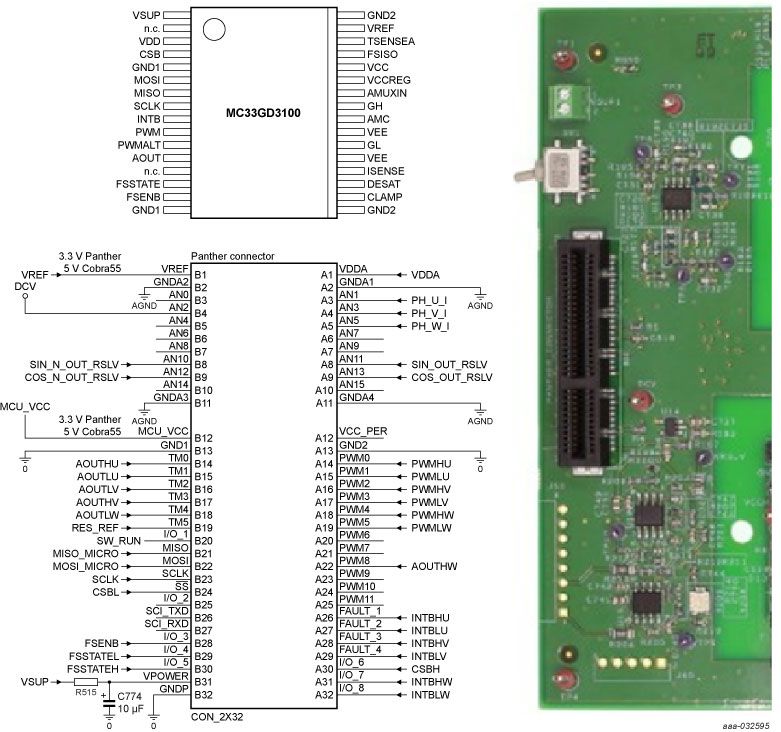
NXP Semiconductors
UM11178
RDGD3100I3PH5EVB three-phase inverter reference design
Test point name Function
FSISLW Not used – for test purposes only
GHU Gate high-side U phase which is the charging pin of IGBT gate
GHV Gate high-side V phase which is the charging pin of IGBT gate
GHW Gate high-side W phase which is the charging pin of IGBT gate
GLU Gate low-side U phase which is the charging pin of IGBT gate
GLV Gate low-side V phase which is the charging pin of IGBT gate
GLW Gate low-side W phase which is the charging pin of IGBT gate
NCLU – NCHW Not used – for test purposes only
Resolver circuit Test points for internal signals of resolver circuit (see schematic for more
information)
SPI DBG SPI signal port for analyzing SPI signals (see schematic for signals)
TSENSEHU TSENSE high-side U phase connected to NTC temperature sense
TSENSEHV TSENSE high-side V phase connected to NTC temperature sense
TSENSEHW TSENSE high-side W phase connected to NTC temperature sense
TSENSELU TSENSE low-side U phase
TSENSELV TSENSE low-side V phase
TSENSELW TSENSE low-side W phase
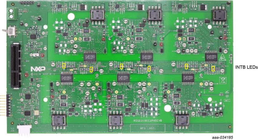
4.2.4 Indicators
The RDGD3100I3PH5EVB evaluation board contains LEDs as visual indicators on the
board.
Figure 5. RDGD3100I3PH5EVB indicator locations
Table 2. RDGD3100I3PH5EVB indicator descriptions
Name Description
INTB LEDs Indicate a GD3100 interrupt has occurred on that gate drive device
UM11178 All information provided in this document is subject to legal disclaimers. © NXP B.V. 2019. All rights reserved.
User manual Rev. 1 — 28 May 2019
9 / 18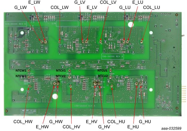
NXP Semiconductors
                                                                                                                       UM11178
                                                           RDGD3100I3PH5EVB three-phase inverter reference design

              4.2.5 Connectors

                    Figure 6. RDGD3100I3PH5EVB connector locations

                    Table 3. RDGD3100I3PH5EVB connector descriptions
                    Name                                                  Description
                    Phase current feedback connector                      Current feedback connections from U, V, and W phases
                    Resolver signals connector                            Resolver excitation signals (see schematic for more information)

              4.2.6 Power supply and jumper configuration

                    Figure 7. Power supply and jumper locations

UM11178                               All information provided in this document is subject to legal disclaimers.        © NXP B.V. 2019. All rights reserved.

User manual                                            Rev. 1 — 28 May 2019
                                                                                                                                                  10 / 18
NXP Semiconductors
UM11178
RDGD3100I3PH5EVB three-phase inverter reference design
Name Function
J2 Low-side phase U VEE select. Negative voltage supply for gate of IGBT.
• 1-2 negative VEE voltage (default) typically −5.0 V to −8.0 V
• 2-3 VEE voltage equal to GND2
J3 High-side phase U VEE select. Negative voltage supply for gate of IGBT.
• 1-2 negative VEE voltage (default) typically −5.0 V to −8.0 V
• 2-3 VEE voltage equal to GND2
J5 High-side phase V VEE select. Negative voltage supply for gate of IGBT.
• 1-2 negative VEE voltage (default) typically −5.0 V to −8.0 V
• 2-3 VEE voltage equal to GND2
J6 Low-side phase V VEE select. Negative voltage supply for gate of IGBT.
• 1-2 negative VEE voltage (default) typically −5.0 V to −8.0 V
• 2-3 VEE voltage equal to GND2
J7 High-side phase W VEE select. Negative voltage supply for gate of IGBT.
• 1-2 negative VEE voltage (default) typically −5.0 V to −8.0 V
• 2-3 VEE voltage equal to GND2
J8 Low-side phase W VEE select. Negative voltage supply for gate of IGBT.
• 1-2 negative VEE voltage (default) typically −5.0 V to −8.0 V
• 2-3 VEE voltage equal to GND2
J100 Used for routing DC voltage from VSUP connection terminal
SJ1 to SJ6 Solder jumpers used for 5.0 V operation connecting VSUP to VDD on each gate
drive device
SW1 Not used (internal purposes only)
VCCHU High-side phase U VCC voltage test point
Isolated positive voltage supply (15 V to 18 V)
VCCHV High-side phase V VCC voltage test point
Isolated positive voltage supply (15 V to 18 V)
VCCHW High-side phase W VCC voltage test point
Isolated positive voltage supply (15 V to 18 V)
VCCLU Low-side phase U VCC voltage test point
Isolated positive voltage supply (15 V to 18 V)
VCCLV Low-side phase V VCC voltage test point
Isolated positive voltage supply (15 V to 18 V)
VCCLW Low-side phase W VCC voltage test point
Isolated positive voltage supply (15 V to 18 V)
VSUP +12 V DC VSUP low voltage positive supply connection (+12 V DC)
VSUP GND VSUP low voltage supply ground connection (GND1)
4.2.7 Gate drive resistors
• RGH - gate high resistor in series with the GH pin at the output of the GD3100 high-
side driver and IGBT gate that controls the turn on current for IGBT gate.
• RGL - gate low resistor in series with the GL pin at the output of the GD3100 low-side
driver and IGBT gate that controls the turn off current for IGBT gate.
• RAMC - series resistor between IGBT gate and AMC input pin of the GD3100 high-
side/low-side driver for gate sensing and Active Miller clamping.
UM11178 All information provided in this document is subject to legal disclaimers. © NXP B.V. 2019. All rights reserved.
User manual Rev. 1 — 28 May 2019
11 / 18NXP Semiconductors
UM11178
RDGD3100I3PH5EVB three-phase inverter reference design
Figure 8. Gate drive resistors for each phase high-side and low-side
4.2.8 IGBT pin connections
Figure 9. IGBT connection pins
Connection name Pin description
COL_HU Collector high-side U phase
COL_HV Collector high-side V phase
COL_HW Collector high-side W phase
COL_LU Collector low-side U phase
COL_LV Collector low-side V phase
COL_LW Collector low-side W phase
E_HU Emitter high-side U phase
E_HV Emitter high-side V phase
E_HW Emitter high-side W phase
UM11178 All information provided in this document is subject to legal disclaimers. © NXP B.V. 2019. All rights reserved.
User manual Rev. 1 — 28 May 2019
12 / 18NXP Semiconductors
UM11178
RDGD3100I3PH5EVB three-phase inverter reference design
Connection name Pin description
E_LU Emitter low-side U phase
E_LV Emitter low-side V phase
E_LW Emitter low-side W phase
G_HU Gate high-side U phase
G_HV Gate high-side V phase
G_HW Gate high-side W phase
G_LU Gate low-side U phase
G_LV Gate low-side V phase
G_LW Gate low-side W phase
NTC1 Negative temperature coefficient resistor connections 1 U, V, and W phase
NTC2 Negative temperature coefficient resistor connections 2 U, V, and W phase
4.3 Schematic, board layout, and bill of materials
The schematic, board layout, and bill of materials for the RDGD3100I3PH5EVB
reference design are available at http://www.nxp.com/RDGD3100I3PH5EVB.
5 Configuring the hardware for startup
Figure 10 presents a typical hardware configuration.
Figure 10. Typical configuration
To configure the hardware as illustrated in Figure 10, complete the following procedure:
1. Assemble IGBT module with water cooling jacket if desired and properly attach to DC
Link capacitor positive and negative high-voltage supply connections across U, V, and
W phases.
2. Attach RDGD3100I3PH5EVB to the IGBT module. Ensure that all board socket
connection pins are properly seated onto the IGBT pin connections. The board socket
pins are intended for easy attachment and deattachment to IGBT module without
damaging IGBT connection pins.
3. Connect motor:
UM11178 All information provided in this document is subject to legal disclaimers. © NXP B.V. 2019. All rights reserved.
User manual Rev. 1 — 28 May 2019
13 / 18NXP Semiconductors
UM11178
RDGD3100I3PH5EVB three-phase inverter reference design
a. Connect output of IGBT module each phase U, V, and W to each of the respective
U, V, W connections on the desired three-phase motor.
b. For running motor in closed loop motor control, connect resolver signals
from motor resolver connection to the resolver pin connections on the
RDGD3100I3PH5EVB. See schematics for J50 header signal connections on the
RDGD3100I3PH5EVB board.
c. For running motor in closed loop motor control, connect current sensors from each
phase U, V, and W (current sensors are not included with RDGD3100I3PH5EVB)
and connect the respective signals from the current sensors to the phase current
feedback pin connections of the RDGD3100I3PH5EVB. See schematics for J40
header signal connections on the RDGD3100I3PH5EVB board.
4. Connect DC power:
a. Connect a low voltage DC power supply to the RDGD3100I3H5EVB at the VSUP
connection terminal (12 V DC with a minimum 1.0 A supply). Ensure that J100
jumper is in place.
b. Connect a low voltage DC supply to MCU controller board and connect USB cable
from MCU controller to desired computer for software driven motor control.
c. Connect high voltage/high current DC supply (use recommended voltage and
current for desired motor) to positive and negative connections on DC Link
capacitor to supply three-phase motor DC link voltage.
5. Attach 2x32 PCIe cable (X-S32SDEV-CON18) supplied with kit to the
RDGD3100I3PH5EVB and MCU controller board such as the MPC5777C-DEVB. This
cable is keyed and is compatible with interface port on MPC5777C-DEVB.
6 Installing and configuring software and tools
6.1 Software development tools
NXP has software development tools available for use with the NXP MPC5777C
development board (DEVB). The development board is intended to provide a platform
for easy customer evaluation of the MPC5777C microcontroller and to facilitate hardware
and software development. The development board can be used for Powertrain/
Inverters/BMS/Automotive ethernet, etc. The latest product information is available at
www.nxp.com/MPC5777C.
List of Development software:
• S32S Design Studio IDE for power architecture:
The S32S design studio for power architecture IDE installed on a Windows PC
workstation enables editing, compiling and debugging of source code designs. SDK
supports several devices including MPC5777C. For more information, refer to S32DS-
PA SDK for power architectures at http://www.nxp.com.
• Automotive Math and Motor Control Library (AMMCL):
Automotive Math and Motor Control Library (AMMCL) is a precompiled software
library containing the building blocks for a wide range of motor control and general
mathematical applications. For more information and to download AMMCL, refer to
Automotive Math and Motor Control Library Set for MPC577xC at http://www.nxp.com.
• FreeMaster 2.0 runtime debugging tool:
FreeMASTER runtime debugging tool is a separate download and can also be
used in conjunction with the MCU code developed with S32DS as a user-friendly real-
time debug monitor, graphical control panel, and data visualization tool for application
UM11178 All information provided in this document is subject to legal disclaimers. © NXP B.V. 2019. All rights reserved.
User manual Rev. 1 — 28 May 2019
14 / 18NXP Semiconductors
UM11178
RDGD3100I3PH5EVB three-phase inverter reference design
development and information management. See FreeMASTER runtime debugging tool
at http://www.nxp.com.
• Motor Control Application Tuning (MCAT):
Motor Control Application Tuning (MCAT) is a FreeMASTER plug-in tool intended
for the development of PMSM FOC and BLDC motor control applications. For more
information and to download MCAT, refer to MCAT at http://www.nxp.com.
• Example code, GD3100 Device Driver notes and GD3100 Device Driver Reference
notes:
GD3100 Device Driver example code REV1.1 provides a basis to get started and
begin software development for the desired motor control. See GD3100 Device Driver
Example Code (REV 1.1 or later) at http://www.nxp.com.
7 References
[1] RDGD3100I3PH5EVB — detailed information on this board, including documentation, downloads, and software and
tools
http://www.nxp.com/RDGD3100I3PH5EVB
[2] GD3100 — product information on Advanced single-channel gate driver for Insulated Gate Bipolar Transistors
(IGBTs)
http://www.nxp.com/GD3100
[3] MPC5777C — ultra-reliable MCU for automotive and industrial engine management
http://www.nxp.com/MPC5777C
[4] MPC5744P — ultra-reliable MCU for automotive and industrial safety applications
https://www.nxp.com/MPC574xP
8 Revision history
Revision history
Rev Date Description
v.1 20190528 Initial version
UM11178 All information provided in this document is subject to legal disclaimers. © NXP B.V. 2019. All rights reserved.
User manual Rev. 1 — 28 May 2019
15 / 18NXP Semiconductors
UM11178
RDGD3100I3PH5EVB three-phase inverter reference design
9 Legal information
default of the applications and the products or of the application or use by
customer’s third party customer(s). NXP does not accept any liability in this
9.1 Definitions respect.
Draft — The document is a draft version only. The content is still under Suitability for use in automotive applications — This NXP
internal review and subject to formal approval, which may result in Semiconductors product has been qualified for use in automotive
modifications or additions. NXP Semiconductors does not give any applications. Unless otherwise agreed in writing, the product is not designed,
representations or warranties as to the accuracy or completeness of authorized or warranted to be suitable for use in life support, life-critical or
information included herein and shall have no liability for the consequences safety-critical systems or equipment, nor in applications where failure or
of use of such information. malfunction of an NXP Semiconductors product can reasonably be expected
to result in personal injury, death or severe property or environmental
damage. NXP Semiconductors and its suppliers accept no liability for
inclusion and/or use of NXP Semiconductors products in such equipment or
9.2 Disclaimers applications and therefore such inclusion and/or use is at the customer's own
risk.
Limited warranty and liability — Information in this document is believed
Export control — This document as well as the item(s) described herein
to be accurate and reliable. However, NXP Semiconductors does not
may be subject to export control regulations. Export might require a prior
give any representations or warranties, expressed or implied, as to the
authorization from competent authorities.
accuracy or completeness of such information and shall have no liability
for the consequences of use of such information. NXP Semiconductors
Evaluation products — This product is provided on an “as is” and “with all
takes no responsibility for the content in this document if provided by an
faults” basis for evaluation purposes only. NXP Semiconductors, its affiliates
information source outside of NXP Semiconductors. In no event shall NXP
and their suppliers expressly disclaim all warranties, whether express,
Semiconductors be liable for any indirect, incidental, punitive, special or
implied or statutory, including but not limited to the implied warranties of
consequential damages (including - without limitation - lost profits, lost
non-infringement, merchantability and fitness for a particular purpose. The
savings, business interruption, costs related to the removal or replacement
entire risk as to the quality, or arising out of the use or performance, of this
of any products or rework charges) whether or not such damages are based
product remains with customer. In no event shall NXP Semiconductors, its
on tort (including negligence), warranty, breach of contract or any other
affiliates or their suppliers be liable to customer for any special, indirect,
legal theory. Notwithstanding any damages that customer might incur for
consequential, punitive or incidental damages (including without limitation
any reason whatsoever, NXP Semiconductors’ aggregate and cumulative
damages for loss of business, business interruption, loss of use, loss of
liability towards customer for the products described herein shall be limited
data or information, and the like) arising out the use of or inability to use
in accordance with the Terms and conditions of commercial sale of NXP
the product, whether or not based on tort (including negligence), strict
Semiconductors.
liability, breach of contract, breach of warranty or any other theory, even if
advised of the possibility of such damages. Notwithstanding any damages
Right to make changes — NXP Semiconductors reserves the right to
that customer might incur for any reason whatsoever (including without
make changes to information published in this document, including without
limitation, all damages referenced above and all direct or general damages),
limitation specifications and product descriptions, at any time and without
the entire liability of NXP Semiconductors, its affiliates and their suppliers
notice. This document supersedes and replaces all information supplied prior
and customer’s exclusive remedy for all of the foregoing shall be limited to
to the publication hereof.
actual damages incurred by customer based on reasonable reliance up to
the greater of the amount actually paid by customer for the product or five
Applications — Applications that are described herein for any of these dollars (US$5.00). The foregoing limitations, exclusions and disclaimers
products are for illustrative purposes only. NXP Semiconductors makes shall apply to the maximum extent permitted by applicable law, even if any
no representation or warranty that such applications will be suitable remedy fails of its essential purpose.
for the specified use without further testing or modification. Customers
are responsible for the design and operation of their applications and
Translations — A non-English (translated) version of a document is for
products using NXP Semiconductors products, and NXP Semiconductors
reference only. The English version shall prevail in case of any discrepancy
accepts no liability for any assistance with applications or customer product
between the translated and English versions.
design. It is customer’s sole responsibility to determine whether the NXP
Semiconductors product is suitable and fit for the customer’s applications
and products planned, as well as for the planned application and use of
customer’s third party customer(s). Customers should provide appropriate
design and operating safeguards to minimize the risks associated with 9.3 Trademarks
their applications and products. NXP Semiconductors does not accept any
liability related to any default, damage, costs or problem which is based Notice: All referenced brands, product names, service names and
on any weakness or default in the customer’s applications or products, or trademarks are the property of their respective owners.
the application or use by customer’s third party customer(s). Customer is
responsible for doing all necessary testing for the customer’s applications NXP — is a trademark of NXP B.V.
and products using NXP Semiconductors products in order to avoid a SMARTMOS — is a trademark of NXP B.V.
UM11178 All information provided in this document is subject to legal disclaimers. © NXP B.V. 2019. All rights reserved.
User manual Rev. 1 — 28 May 2019
16 / 18NXP Semiconductors
UM11178
RDGD3100I3PH5EVB three-phase inverter reference design
Tables
Tab. 1. PCIe connector pin definitions .......................... 6 Tab. 3. RDGD3100I3PH5EVB connector
Tab. 2. RDGD3100I3PH5EVB indicator descriptions ..................................................... 10
descriptions ....................................................... 9
Figures
Fig. 1. RDGD3100I3PH5EVB .......................................1 Fig. 6. RDGD3100I3PH5EVB connector locations ..... 10
Fig. 2. RDGD3100I3PH5EVB three-phase inverter Fig. 7. Power supply and jumper locations .................10
board voltage domains and interfaces .............. 4 Fig. 8. Gate drive resistors for each phase high-
Fig. 3. Gate driver pinout and board interface side and low-side ............................................ 12
connection PCIe 2×32 .......................................6 Fig. 9. IGBT connection pins ......................................12
Fig. 4. RDGD3100I3PH5EVB test points ..................... 8 Fig. 10. Typical configuration ....................................... 13
Fig. 5. RDGD3100I3PH5EVB indicator locations ......... 9
UM11178 All information provided in this document is subject to legal disclaimers. © NXP B.V. 2019. All rights reserved.
User manual Rev. 1 — 28 May 2019
17 / 18NXP Semiconductors
UM11178
RDGD3100I3PH5EVB three-phase inverter reference design
Contents
1 Introduction ......................................................... 2
2 Finding kit resources and information on
the NXP web site ................................................ 2
2.1 Collaborate in the NXP community ....................2
3 Getting started .................................................... 2
3.1 Kit contents ........................................................3
3.2 Additional hardware ........................................... 3
3.3 Windows PC workstation ...................................3
3.4 Software .............................................................3
4 Getting to know the hardware ........................... 3
4.1 Kit overview ....................................................... 3
4.1.1 RDGD3100I3PH5EVB features ......................... 3
4.1.2 Voltage domains, GD3100 pinout, logic
header, and IGBT pinout ................................... 4
4.2 Featured components ........................................4
4.2.1 Advanced IGBT gate driver ............................... 4
4.2.1.1 General description ............................................4
4.2.1.2 GD3100 features ............................................... 5
4.2.2 GD3100 pinout and MCU interface pinout ......... 5
4.2.3 Test points ......................................................... 8
4.2.4 Indicators ........................................................... 9
4.2.5 Connectors .......................................................10
4.2.6 Power supply and jumper configuration ...........10
4.2.7 Gate drive resistors ......................................... 11
4.2.8 IGBT pin connections ...................................... 12
4.3 Schematic, board layout, and bill of materials .. 13
5 Configuring the hardware for startup ..............13
6 Installing and configuring software and
tools ....................................................................14
6.1 Software development tools ............................ 14
7 References ......................................................... 15
8 Revision history ................................................ 15
9 Legal information .............................................. 16
Please be aware that important notices concerning this document and the product(s)
described herein, have been included in section 'Legal information'.
© NXP B.V. 2019. All rights reserved.
For more information, please visit: http://www.nxp.com
For sales office addresses, please send an email to: salesaddresses@nxp.com
Date of release: 28 May 2019
Document identifier: UM11178You can also read


