Voltage Translation Buying Guide - Auto-Direction Sensing Direction Controlled Application-Specific - Texas Instruments

 
CONTINUE READING
Voltage Translation Buying Guide - Auto-Direction Sensing Direction Controlled Application-Specific - Texas Instruments
Voltage Translation
Buying Guide
Auto-Direction Sensing • Direction Controlled • Application-Specific

ti.com/voltage-level-translation I 2Q 2021
Table of contents/overview Voltage translation buying guide

   Overview                                                                                 Auto bi-directional translators
   Introduction ....................................................................3       LSF family (Passive FET).............................................. 10

   Voltage translation portfolio.............................................4              TXB family (Buffer based)............................................. 11

   Direction controlled translators                                                         TXS family (Switch based)............................................ 12

   AXC family (0.65 V to 3.6 V) ...........................................5                Application specific...................................................... 13

   AVC family (1.2 V to 3.6 V)..............................................6               Uni-directional translators
   LVC family (1.65 V to 5.5 V)............................................ 7               2N7001T (Dual-supply buffer translator)........................14

   Application specific.........................................................8           AVC family (Dual-supply translator) ...............................15

   GTL/TTL translators.......................................................9              AUP1T family (Single-supply logic)................................15

                                                                                            LVxT family (Single-supply logic)....................................16

                                                                                            Additional resources
                                                                                            Over-voltage, TTL, and open-drain compatible devices....... 17

What class of voltage translator should I use?                                              When to use an auto bi-directional translator?
                                                                                            Some interfaces require that the I/O pins of each device
Know your interface? Jump to our quick selection table.
                                                                                            be open-drain or open-collector so that any device can
Texas Instruments (TI) offers a wide range of voltage                                       start to transmit on the bus. This is typically required for
translators to fit the needs for a system’s design. The                                     multi-controller, multi-peripheral protocols; such as I2C and
portfolio is broken into three main classes: direction                                      SMBUS. Auto bi-directional voltage translators can ‘auto-
controlled, auto bi-directional, and uni-directional.                                       sense’ the intended direction of communication and operate
                                                                                            accordingly; however these translators are slower and have
When to use a direction-controlled translator?
                                                                                            less drive strength compared to other classes of translators.
Direction-controlled translators are the most flexible, easy-
                                                                                            Search auto bi-directional on ti.com | Skip to the auto-
to-use, and offer the best signal integrity. They are best for
                                                                                            directional overview.
one-to-one communication between devices such as RGMII,
and with protocols featuring one controller that determines                                 When to use a uni-directional translator?
when devices will transmit on the bus; such as in SPI and
                                                                                            As their name suggested, uni-directional translators are best
UART. Search direction controlled on ti.com | Skip to the                                   when transmitted signals only need to go one direction.
direction-controlled overview.                                                              Typical examples are reset signals and clock synchronization
                                                                                            signals. Search uni-directional on ti.com | Skip to the
                                                                                            uni-directional overview.

Voltage Translation Buying Guide		                                                      2                                                    2Q 2021 I Texas Instruments
Overview Introduction

Introduction                                                                  Translation devices can be found in almost every market,
                                                                              including: consumer electronics, portable electronics,
To help system designers interconnect devices operating
                                                                              computing, automotive, industrial and networking
on different voltage rails that have different IO voltage levels,
                                                                              applications. Wherever the need exists to interface lower
TI offers a comprehensive voltage translation portfolio
                                                                              operating processors with higher operating peripherals.
including dual-supply level translators; auto-direction sensing
translators for both push-pull buffered and open-drain
applications; and hybrid application-specific translators
optimized for today’s constantly emerging signal standards.

                                                             Voltage
                                                           translators

                Direction                                      Auto
                controlled                                bi-directional                                      Uni-directional

      General                 Application       General                       Application            Single                      Dual
      purpose                  specific         purpose                        specific              supply                     supply

                  VCCA VCCB                                   VCCA VCCB                        VCC                  VCC                  VCCA VCCB

                    DIR

Direction controlled translators                                              Auto bi-directional translators
Direction Controlled translators performs non-inverting up or                 Auto bi-directional translators are a class of voltage
down translation of a uni-directional signal. These translators               translators, which are available in dual supply configurations.
have one or more direction control pins that allow the                        Yet unlike the direction controlled translators they
designer to configure which pins are inputs and outputs. This                 automatically sense the direction of the signal without the
enables simultaneous up and down translation on one device                    need for a direction control pin.
and gives the user more flexibility.                                          Across the three families within the class there are a number
Many devices within this class are available with Bus Hold,                   of trade-offs including drive-strength, data rate, and multi-
which allows the device to retain the last known state of                     voltage translation. The wide range of available functionalities
the output when the inputs are floating or become high                        gives the designer a number of parts to choose from TI’s
impedance. Bus Hold feature is indicated by “H” in the part                   portfolio to suit their needs.
number. More info about bus-hold circuits.
                                                                              Benefits of auto bi-directional:
Benefits of direction controlled:                                             • Works with bi-directional signals.
• Buffered output for high drive strength.                                    • Devices available that have been optimized for common
• One or more direction control pins.                                           interfaces.

• Devices available that have been optimized for common                       • Works with both open-drain and push-pull interfaces.
  interfaces.                                                                 • Design flexibility with external pull-up resistors.
• Bus Hold functionality available.

Voltage Translation Buying Guide		                                        3                                               2Q 2021 I Texas Instruments
Overview Voltage translation portfolio

Uni-directional translators                                                         Benefits of uni-directional:

This class of translators performs a single direction, non-                         • Single supply translators provide simplicity in system
                                                                                      design.
inverting up or down translation of an incoming signal at the
input of a device to the output of the device.                                      • Dual supply translators provide dynamic operating range
                                                                                      for voltage translation.
Single supply translators only have one supply voltage, which
                                                                                    • Voltage translating logic gates achieve two functions
provides the reference level for the output to track. Single
                                                                                      in one chip.
supply translators include translating buffers, as well as
translating logic gates. Translating logic gates have built-in
logic functionality, and at the same time perform up or down
voltage translation. Dual supply translators have two supply
voltages, one at the VCC level of the input signal, the other at
the VCC level of the output signal.

Overview of device families

 Family                       AXC              AVC                 LVC              LSF                 TXB              TXS             AUP                  LV1T
 Class                                  Direction controlled                                       Auto directional                            Uni-directional
                                                                               Open-drain or
 Interfaces supported                        Push-pull
                                                                                 push-pull
                                                                                                      Push-pull        Open-drain                Push-pull

 VCC (V)                 0.65 to 3.6         1.2 to 3.6        1.65 to 5.5       0.9 to 5.5           1.2 to 5.5       1.2 to 5.5      0.9 to 3.6        1.65 to 5.5
 Drive strength (mA)          12                12                    32             —                  0.02             0.02              4                     8
 Max data rate (Mbps)         380              340                 300               200                 140              100            380                  100
 Max bits                      8                32                    16              8                   8                8               1                     1

                                                                       Select by interface
 Interface                     2 Ch                            4 Ch                         6 Ch                          8 Ch                        16 Ch
                                                          SN74AXC4T774
 SPI                               —
                                                            TXB0104
                                                                                              —                       SN74AXC8T245              SN74AVC16T245

                                                          SN74AXC4T774                                                SN74AVC8T245
 UART                              —
                                                            TXB0104
                                                                                              —
                                                                                                                      SN74AXC8T245
                                                                                                                                                SN74AVC16T245

                                                          SN74AXC4T774
 JTAG                              —
                                                            TXB0104
                                                                                              —                       SN74AXC8T245              SN74AVC16T245

                                                            TXB0104
 I2S                               —
                                                          SN74AXC4T245
                                                                                              —                       SN74AXC8T245              SN74AVC16T245

                              TXS0102                       TXS0104E                                                    TXS0108E
 I2C                          LSF0102                        LSF0204
                                                                                              —
                                                                                                                         LSF0108
                                                                                                                                                        —

                              TXS0102                       TXS0104E                                                    TXS0108E
 MDIO                         LSF0102                        LSF0204
                                                                                              —
                                                                                                                         LSF0108
                                                                                                                                                        —

                              TXS0102                       TXS0104E                                                    TXS0108E
 SMBus                        LSF0102                        LSF0204
                                                                                              —
                                                                                                                         LSF0108
                                                                                                                                                        —

 RMII/RGMII                        —                           —                           TXB0106                    SN74AXC8T245              SN74AVC16T245
 Quad-SPI                          —                           —                           TXB0106                         —                            —
 SDIO                              —                        LSF0204                           —                         LSF0108                         —

Voltage Translation Buying Guide		                                              4                                                    2Q 2021 I Texas Instruments
Direction controlled translators 0.65 V to 3.6 V

General purpose                                                                          Key features
AXC family I Search AXC on TI.com                                                        • Fully configurable rails – each VCC
The AXC direction controlled level translation family is the newest addition to TI’s       rail is fully configurable from 0.65 V to
selection of direction controlled voltage translators. Designed for an ultra-low VCC       3.6 V.
range between 0.65 V to 3.6 V, making it the lowest voltage level translator available   • Up to 380-Mbps data rate support.
in the industry. This allows the device to communicate with advance processors
                                                                                         • VCC isolation – if either VCC is at
operating at low voltage nodes of 0.7 V, 0.8 V or 0.9 V. The wide VCC range also
accommodates the industry standard voltage nodes 1.2 V, 1.8 V, 2.5 V, and 3.3 V            ground, all inputs and outputs enter a
still commonly found in processors and peripherals.                                        high impedance state.

The 4-bit and 8-bit device features a second direction control pin allowing two          • IOFF supports operation in partial-
independent banks of buses, 2-bit and 4-bit respectively, on one device. This              power-down mode.
allows more control in how the device can be used through simultaneous up and            • Independent power supply sequencing.
down translation and, ideally, reduces the BOM count. Additionally these devices
include an output enable pin, to put all outputs in a high impedance state which         Benefits
also reduces power consumption.
                                                                                         • Wide VCC range enables
All devices in the family were rigorously designed to ensure glitch-free power             communication with most advance
sequencing across hundreds of possible start up or shut down conditions. This              processors and FPGAs.
allows either supply rail to be powered on or off, in any order without causing a
                                                                                         • High data rate while supporting lower
glitch at the output. To learn more on independent power supply sequencing read
                                                                                           voltages.
our application report on Power Sequencing for AXC Family Devices.
                                                                                         • Glitch-free performance ensures
                                                                                           system reliability on power-up and
                          V CCA                            V CCB
                                                                                           power-down.

                                                                                         Package options
                                                                                         • X2SON         • SOT-5X3
           Processor                                                       Peripheral
                                                                                         • SOT-23        • TSSOP
                           DIR
                                                                                         • SC70          • VQFN
                                  SN74AXCxT45/245
                                                                                         Applications
                                                                                         • Data center switches.
                       0.7 V                                       3.3 V
                                                                                         • Baseband unit and remote radio unit.
                                                                                         • Server motherboards.
                                  VCCA DIR1 DIR2   VCCB
                                  A1                  B1
                                                                                         • IP camera.
                                  A2                  B2

            RMII
                                  A3                  B3
                                                                                 RMII
                                                                                         • Programmable logic controller.
                                  A4                  B4
            MAC                   A5                  B5                         PHY     • Notebook PCs.
                                  A6                  B6
                                  A7                  B7
                                  A8                  B8                                 • Enterprise SSD.
                                       SN74AXC8T245
                                                                                         • Infotainment and cluster.
                                                                                         • ADAS.

Voltage Translation Buying Guide		                                              5                        2Q 2021 I Texas Instruments
Direction controlled translators 1.2 V to 3.6 V

AVC family I Search AVC on TI.com                                                                       Key features
The AVC family of voltage translators use two separate configurable power supply                        • 500-Mbps max data rate on 1T/2T
rails to enable asynchronous communications between A and B data ports, or vise-                          and 320 Mbps on 8T and higher.
versa depending on the direction pin. The A port is designed to track VCCA while the
                                                                                                        • Control input levels, VIH / VIL, are
B port is designed to track VCCB. Both VCCA and VCCB are configurable from 1.2 V to
3.6 V.                                                                                                    referenced to VCCA voltage.

These devices are fully specified for partial-power-down applications using IOFF. The                   • Fully configurable dual-rail design
IOFF circuitry disables the outputs, preventing damaging current backflow through                         allows each port to operate over full
the device when it is powered down.                                                                       1.2 V to 3.6 V power-supply range.

                                                                                                        • IOFF supports operation in partial-
                                                                                                          power-down mode.
                                   V CCA                     V CCB
                                                                                                        • VCC isolation ensure that if either VCC
                                                                                                          input is at ground both ports are in
                                                                                                          high impedance.

                Processor                                                    Peripheral
                                                                                                        Package options
                                   DIR
                                                                                                        • DSBGA         • TVSOP
                                           SN74AVCxT45/245                                              • SC70          • UQFN
                                                                                                        • SM8           • VQFN
                                                                                                        • SOT-23        • US8
                                                                                                        • SOT           • BGA MicroStar
 Popular devices            Bits           VCCA range          VCCB range            Data rate (Mbps)   • TSSOP           Junior™
 SN74AVC1T45                 1             1.2 to 3.6           1.2 to 3.6                 500
 SN74AVC8T245                8             1.2 to 3.6           1.2 to 3.6                 320
 SN74AVC32T245              32             1.2 to 3.6           1.2 to 3.6                 320

Voltage Translation Buying Guide		                                             6                                        2Q 2021 I Texas Instruments
Direction controlled translators 1.65 V to 5.5 V

LVC family I Search LVC on TI.com                                                                    Key features
The LVC family of non-inverting voltage translators use two separate configurable                    • High drive ability, up to 32 mA of
power supply rails to enable asynchronous communications between A port inputs                         current.
and B port outputs, or vise-versa depending on the direction pin. The A port is
                                                                                                     • Up to 420-Mbps max data rate on
designed to track VCCA while the B port is designed to track VCCB. Both VCCA and
                                                                                                       1T/2T.
VCCB are configurable from 1.65 V to 5.5 V.
                                                                                                     • Control input levels, VIH / VIL, are
These devices were designed to have high drive strength, of up to 32 mA, while
                                                                                                       referenced to VCCA voltage.
maintaining low static and dynamic power consumption.
                                                                                                     • Fully configurable dual-rail design
                                                                                                       allows each port to operate over full
                                   V CCA                     V CCB                                     1.65-V to 5.5-V power-supply range.
                                                                                                     • IOFF supports operation in partial-
                                                                                                       power-down mode.
                                                                                                     • VCC isolation ensure that if either VCC
                Processor                                                 Peripheral                   input is at ground both ports are in
                                   DIR                                                                 high impedance.

                                           SN74AVCxT45/245                                           Package options
                                                                                                     • SO            • VSSOP
                                                                                                     • SOIC          • VQFN
                                                                                                     • SSOP          • SM8
 Popular devices            Bits           VCCA range          VCCB range         Data rate (Mbps)
 SN74LVC1T45                 1             1.65 to 5.5          1.65 to 5.5             420          • TSSOP         • DSBGA
 SN74LVC8T245                8             1.65 to 5.5          1.65 to 5.5             320          • TVSOP         • BGA MicroStar
 SN74LVC16T245              16             1.65 to 5.5          1.65 to 5.5             320                            Junior™
                                                                                                     • SC70

Voltage Translation Buying Guide		                                            7                                      2Q 2021 I Texas Instruments
Direction controlled translators Application specific

Application specific I Search application specific solutions on                             Interfaces supported
TI.com
                                                                                            • SPI
TI’s portfolio of direction controlled translators includes devices that have been
                                                                                            • UART
optimized for use in common communication interfaces used by processors and
peripherals. Direction controlled translators are best suited for interfaces where the      • JTAG
direction of each data line is fixed, such as SPI or UART. If the data lines are            • RMII/RGMII
bi-directional it is best to go with an auto bi-directional voltage translator such as      • I2S
TXS, TXB or LSF.
                                                                                            • IC-USB
                                                                                            • Audio
                                                                                            • SD/MMC
     SPI controller                                           SPI peripheral
                       CLK                                    CLK
                      COPI                                    COPI
                      CIPO                  AVC4T774
                                                              CIPO
                       CS1                                    CS
                       CS2
                       CS3

                                                              SPI peripheral
                                                              CLK
                                                              COPI
                                            AVC4T774          CIPO
                                                              CS

 Popular devices       Interface      Bits             VCCA range              VCCB range
 SN74AVC4T774             SPI           4               1.2 to 3.6             1.2 to 3.6
 SN74AVCA406          SD and MMC        7               1.2 to 3.6             1.2 to 3.6
 SN74AVC2T872           IC-USB          2               1.1 to 3.6             1.1 to 3.6

Voltage Translation Buying Guide		                                   8                                     2Q 2021 I Texas Instruments
Direction controlled translators GTL / TTL translators

GTL / TTL translators I Search GTL / TTL translators on TI.com                                          Package options
This class of voltage translators includes the GTL and GTLP families as well as the                     • TSSOP
legacy FB and TTL families. These devices were designed to allow communication
                                                                                                        • SC70
between Low Voltage Transistor Transistor Logic (LVTTL) and Gunning Transceiver
                                                                                                        • HLQFP
Logic (GTL) interface levels. These devices have reduced voltage swing that allows
them to have a fast data rate, high drive strength and low noise. GTL devices are                       • QFP
best suited for backplane bus translation with most of the Intel® processors.                           • SSOP
These devices come in both direction controlled and auto bi-directional                                 • SOIC
configurations. Additionally a number of the parts within this class are specifically                   • TVSOP
designed for common interfaces.

                                                         GTL2014PW

                                                    B0           +
                                                                 -
                                                                                     A0

          DIR 1                   14 VCC
           B0 2                   13 A0
                                                    B1           +
                                                                 -                   A1
           B1 3                   12 A1
          VREF 4   GTL2014PW      11 GDN
           B2 5                   10 A2
                                                    B2           +
                                                                                     A2
           B3 6                   9    A3                        -

         GND 7                    8    GND

                                                    B3           +
                                                                 -
                                                                                     A3

                                                         VREF          DIR

Popular devices        Bits           VCC range             VREF range                 Class
SN74GTL2014              4            3.0 to 3.6            0.5 to 1.65          Direction controlled
SN74GTL2003              8            0.95 to 5.5           0.95 to 5.5          Auto bi-directional
SN74GTL2007             12            3.0 to 3.6                0.5 to 1.8       Auto bi-directional

Voltage Translation Buying Guide		                                           9                                    2Q 2021 I Texas Instruments
Auto bi-directional translators Passive FET

General purpose                                                                             Key features
LSF family I Search LSF on TI.com                                                           • Provides bidirectional voltage
The LSF family are bi-directional voltage level translators operational from 0.8 V            translation.
to 4.5 V (VREF_A) and 1.8 V to 5.5 V (VREF_B). This allows bi-directional voltage           • Less than 1.5-ns max propagation
translations between 1.0 V and 5.0 V without the need for a direction terminal                delay.
in open-drain or push-pull applications. LSF family supports level translation
                                                                                            • High-speed translation > 100 MHz.
applications with transmission speeds greater than 100 Mbps for open-drain
systems utilizing a 15-pF capacitance and 200-Ω pull-up resistor.                           • Supports hot insertion.

The low RON of the switch allows connections to be made with minimal propagation            • 5-V tolerance I/O port to support
delay and signal distortion. Assuming the higher voltage is on the Bn port.                   TTL.
                                                                                            • Low RON reduces signal distortion.
Voltage translation with the LSF family
                                                                                            • Flow-through pinout for easy PCB
                                                                                              routing.
                            VCCA                   VCCB
                                                                                            • ESD performance tested per
                                                                                              JESD 22.

                                                                                            Package options
          Processor                                            Peripheral
                                                                                            • VSSOP
                                                                                            • TSSOP
                                                                                            • DSBGA
                                                                                            • UQFN
                                                                                            • VQFN
Popular devices        Bits        VCCA range         VCCB range         Data rate (Mbps)
                                                                                            • SM8
LSF0101                 1          0.95 to 5.0        1.65 to 5.0              200
LSF0204                 4           0.8 to 4.5         1.8 to 5.5              200          • X2SON
LSF0108                 8          0.95 to 5.0        1.65 to 5.0              200          • SON

Voltage Translation Buying Guide		                                  10                                     2Q 2021 I Texas Instruments
Auto bi-directional translators Buffer based

TXB family I Search TXB on TI.com                                                                 Key features
The TXB family of non-inverting translators uses two separate configurable power-                 • Optimized for push-pull interfaces
supply rails to enable bi-directional translation. In the TXB010x family, the A port is
                                                                                                  • 140-Mbps max data rate
designed to track VCCA. VCCA accepts any supply voltage from 1.2 V to 3.6 V. The B
port is designed to track VCCB. VCCB accepts any supply voltage from 1.65 V to 5.5 V.             • Output Enable (OE) input circuit
                                                                                                    referenced to VCCA
The TXB030x family of devices functions similar to the TXB010x; however TXB030x
has fully symmetrical supply voltages, accepting 0.9 V to 3.6 V on both supply                    • Low power consumption
ports.                                                                                            • TXB010x: 1.2 V to 3.6 V on A-port
                                                                                                    and 1.65 V to 5.5 V on B-port
A guide to voltage translation with TXB-type translators
                                                                                                    (VCCA ≤ VCCB)
                                 V CCA                V CCB                                       • TXB030x: 0.9 V to 3.6 V on both
                                                                                                    A-Port and B-Port

                                                                                                  Package options
              Processor                                                Peripheral                 • X2SON
                                                                                                  • UQFN
                                                                                                  • TSSOP
                                            TXB030x
                                                                                                  • VQFN
                                                                                                  • DSBGA
                                                                                                  • SC70
Popular devices           Bits           VCCA range     VCCB range             Data rate (Mbps)
TXB0102                    2             1.2 to 3.6      1.65 to 5.5                 100          • SOT-23
TXB0302                    2             0.9 to 3.6       0.9 to 3.6                 140          • SOT-5X3
TXB0108                    8             1.2 to 3.6      1.65 to 5.5                 100
                                                                                                  • SOIC
                                                                                                  • BGA MicroStar Junior™

Voltage Translation Buying Guide		                                       11                                      2Q 2021 I Texas Instruments
Auto bi-directional translators Switch based

TXS family I Search TXS on TI.com                                                                 Key features
The TXS family of non-inverting auto bi-directional translators uses two separate                 • Works with both open-drain and
configurable power-supply rails. The A port is designed to track VCCA. The B port                   push-pull drivers.
is designed to track VCCB. VCCA must be less than or equal to VCCB. This allows for               • Max data rates:
low-voltage bi-directional translation between any of the 1.8 V, 2.5 V, 3.3 V, and 5 V
                                                                                                    o 24 Mbps (push-pull).
voltage nodes.
                                                                                                    o 2 Mbps (open-drain).
One-shot circuitry inside the device helps in rise and fall time edge acceleration.
                                                                                                    o 110 Mbps for TXS0108E.
A guide to voltage translation with TXS-type translators
                                                                                                  • 1.65 V to 3.6 V on A-port and 2.3 V
                                                                                                    to 5.5 V on B-port (VCCA ≤ VCCB).
                                 V CCA                 V CCB                                      • TXS0108: 1.2 V to 3.6 V on A-port
                                                                                                    and 1.65 V to 5.5 V on B-port.
                                                                                                  • No power supply sequencing
                                                                                                    required.
              Processor                                                Peripheral                 • IEC 61000-4-2 ESD protection on
                                                                                                    B-port for “E” suffix devices.

                                             TXS010x                                              Package options
                                                                                                  • VSSOP
                                                                                                  • TSSOP
Popular devices           Bits           VCCA range     VCCB range             Data rate (Mbps)   • DSBGA
TXS0101                    1             1.65 to 3.6      2.3 to 5.5                 24
                                                                                                  • UQFN
TXS0104E                   4             1.65 to 3.6      2.3 to 5.5                 24
TXS0108E                   8             1.2 to 3.6      1.65 to 5.5                 110          • QFN
                                                                                                  • SM8
                                                                                                  • X2SON
                                                                                                  • SON

Voltage Translation Buying Guide		                                       12                                     2Q 2021 I Texas Instruments
Auto bi-directional translators Application specific

Application specific I Search application specific solutions on                                             Interfaces supported
TI.com
                                                                                                            • SPI, UART, and JTAG
TI’s portfolio of auto bi-directional translators includes a number of devices that have
                                                                                                            • I2S
been optimized for use in common communication interfaces used by processors
and peripherals. Auto bi-directional translators are best suited in interfaces with truly                   • Quad-SPI
bi-directional data lines such as I2C and SIM Cards.                                                        • I2C, SMBus, and MDIO

A guide to voltage translation with TXS-type translators                                                    • SD/MMC
                                                    VBAT                                                    • SIM card

                    SCK                                                            3-V or 1.8-V
                                            I2C                                      SIM Card
                    SDA                  control                    VSIM1
                                          logic          LDO                           V CC          GND
                                                                  SIM1_RST
                                                                                      Reset           VPP
                  SIM_RST                                         SIM1_CLK
                                                                                       CLK            I/O

                  SIM_CLK                                                               NC            NC
                                                   Translator
                                                                  SIM1_I/O
                  SIM_I/O

  Baseband          V_I/O                            V CC
                                                                                   3-V or 1.8-V
                   RSTX                                                              SIM Card
                                                         LDO        VSIM2
                    IRQ                                                                VCC           GND
                                                                  SIM2_RST
                    CLK                                                               Reset           VPP
                                                                  SIM2_CLK
                    BSI                                                                CLK            I/O

                          OE                       Translator                           NC            NC
                                                                  SIM2_I/O
                      GND

                                        TXS02326
                    SDN

Popular devices                Interface           Bits         VCCA range                    VCCB range
TXS02612                         SDIO                4          1.1 to 3.6                    1.1 to 3.6
TXS02326A                      SIM Card              6          1.7 to 3.3                    2.3 to 5.5
TXS0202                           I2C                2          1.65 to 3.6                   1.65 to 3.6

Voltage Translation Buying Guide		                                            13                                         2Q 2021 I Texas Instruments
Uni-directional translators Dual-supply buffer translator

1-Bit dual-supply buffered voltage signal level shifter                                                                       Key features
2N7001T I Search 2N on TI.com                                                                                                 • 1.65 V to 3.6 V on supply ports
TI’s newest addition to voltage translation is the 2N7001T, a single-bit uni-                                                   with independent sequencing.
directional buffered voltage level shifter that uses two separate power supply                                                • 12 mA of output drive current.
rails for up or down translation. Designed for simplicity, the 2N7001T is a single
component that replaces the multiple components in traditional discrete level                                                 • Up to 100-Mbps data rate.
shifting implementations which helps in reducing design complexity, leakage and                                               • VCC isolation feature.
component count while improving signal performance. This allows for easier layout,
                                                                                                                              • Partial power down – prevents
as well as a great reduction in the space taken up by the level shifting circuit.
                                                                                                                                excess current draw when either
The device is capable of up to 100-Mbps data, and low leakage current reduces                                                   supply rail is powered down.
power consumption. Inherent VCC isolation improves the robustness of the design,
                                                                                                                              • ESD protection:
and removes the need for power sequencing. This allows the designer more
flexibility in power supply design as discreet implementation may require power                                                 o 2000-V human body model.
supply sequencing.
                                                                                                                                o 1000-V charged-device model.
Other advantages over discrete implementation include improved signal
performance through fast deterministic rise and fall times. The 2N7001T ensure                                                Benefits
system stability through glitch free performance.                                                                             • Integrated solution saves space and
Advantages of TI’s integrated 2N7001T level shifter                                                                             makes for easier board layout than
                                                                                                                                discrete implementation.
                                                                                                                              • High data rate while supporting most
                         Discrete solution                                                 Chip based solution                  industry standard voltage levels.
                         V CC        V CC                                                                                     • Glitch-free performance ensures
                                                                                             V CCA   V CCB
                   Rup                                                                                                          system reliability on power-up
Processor

                                                                               Processor
                                                     Peripheral

                                                                                                                 Peripheral

            V IN                            V OUT                                                                               and power-down.
                                                                                                2N7001T

                                                                                                                              Package options
                                                                                               1 component
                                                                                                 (~4mm2)                      • X2SON
                         4 components
                          (~58.5mm2)                                                                                          • SC70

                                                                                                                              Applications
                                                    1.8 V                   3.3 V                                             • Notebook PCs
                                                                                                                              • LCD TV

                                  Input                                                    Output                             • Grid communication
                                                                                                                              • Programmable logic controllers

                                                                  2N7001T

Voltage Level Translation Guide		                                                                     14                                      2Q 2021 I Texas Instruments
Uni-directional translators Dual-supply translator/single-supply logic

AVC family I Search AVC on TI.com                                                                                    Key features
The uni-directional version of the AVC devices uses two separate configurable                                        • 380-Mbps max data rate.
power-supply rails to enable asynchronous communication between B-port
                                                                                                                     • Wide operating VCC range of 0.9 V
inputs and A-port outputs. The A port is designed to track VCCA while the B port is
                                                                                                                       to 3.6 V.
designed to track VCCB. Both VCCA and VCCB are configurable from 0.9 V to 3.6 V.
The SN74AVC2T244/SN74AVC4T234 offers Input hysteresis to allow slow input                                            • 3.6-V I/O tolerant to support
transition and better switching noise                                                                                  mixed-mode signal operation.
                                                     0.9 V       3.3 V
immunity at input. It offers very low                                                                                • Input hysteresis allows slow
static and dynamic power consumption                                                                                   input transition and better.
across the entire VCC range of 0.9 V to                      Input                                          Output
3.6 V, making it the ideal translator for                                                                            Package options
battery powered portable electronics                                                                                 • X2SON
applications.                                                           SN74AVC2T244/4T234
                                                                                                                     • µCSP

Popular devices               Bits             VCCA range               VCCB range              Data rate (Mbps)
SN74AVC2T244                   2                0.9 to 3.6               0.9 to 3.6                    380
SN74AVC4T234                   4                0.9 to 3.6               0.9 to 3.6                    380

AUP1T family I Search AUP on TI.com                                                                                  Key features
AUP technology is the Advanced Ultra-Low Power logic technology, designed to                                         • Low power consumption:
suit low power systems. The SN74AUP1Txx devices are designed for logic level                                           ICC = 0.5 μA.
translation applications with input switching levels that accept 1.8-V LVCMOS
                                                                                                                     • Schmitt-Trigger input: ΔVT = 210 mV,
signals, while operating from either a single 3.3-V or 2.5-V VCC supply. The
                                                                                                                       reject input noise.
AUP1T34 is a dual-supply level translator that operates from 0.9 V to 3.6 V.
                                                                                                                     • Nine configurable gate logic functions
The SN74AUP1Txx with configurable logic function (‘57,’58,’97,’98) can be easily
                                                                                                                       plus standard logic functions.
configured to perform up to nine common gate functions.
                                                                                                                     • ESD performance tested per JESD 22
                                                                                                                       o 2000-V human-body model
                                                               Single-supply translators
                                                                                                                         (A114-B, Class II).
                                                                                                                       o 1000-V charged-device model
                                                                                                                         (C101).
                  Processor                                                           Peripheral

                                                                                                                     Package options
                                                                                                                     • DSBGA
                                                  SN74AUP1Txx
                                                                                                                     • SON
                                                                                                                     • SC70
Popular devices                       Description                    VCCB range                 Data rate (Mbps)
                                                                                                                     • SOT-23
SN74AUP1T00                        NAND gate translator               2.3 to 3.6                      380
SN74AUP1T34                     Dual-supply translator                0.9 to 3.6                      380
SN74AUP1T97                   Configurable gate translator            2.3 to 3.6                      510

Voltage Level Translation Guide		                                                          15                                          2Q 2021 I Texas Instruments
Uni-directional translators Single-supply logic

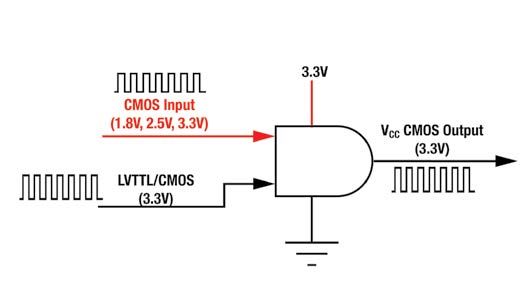
LV family I Search LV on TI.com                                                                       Key features
SN74LV1T is a low-voltage single-supply CMOS logic gate that operates over a                          • Single-supply voltage 1.8-V to
wide voltage range enabling the generation of a large number of desired output                          5.0-V VCC.
levels to connect to controllers or processors using TTL compatible input levels.
                                                                                                      • Operating range of 1.8 V to 5.5 V.
The output level is referenced to the supply voltage and is able to support 1.8-V,
                                                                                                      • Up translation:
2.5-V, 3.3-V, and 5-V CMOS levels.
                                                                                                        o 1.2 V to 1.8 V; 1.8 V to 2.5 V.
The input is designed with a lower threshold circuit to match 1.8-V input logic at
VCC = 3.3 V and can be used in 1.8-V to 3.3-V or 3.3-V to 5-V level up translation.                     o 1.8 V to 3.3 V; 3.3 V to 5.0 V.
In addition, the 5-V tolerant input pins enable down translation (e.g. 3.3-V to 2.5-V                 • Down translation:
output at VCC = 2.5 V).                                                                                 o 3.3/2.5 V to 1.8 V.
The SN74LV1T is designed with current-drive capability of 8 mA to reduce line                           o 5.0/3.3 V to 2.5 V.
reflections, overshoot, and undershoot caused by high-drive outputs.
                                                                                                        o 5.0 V to 3.3 V.

                                                                                                      • Supports standard logic pinouts.
                                                    3.3 V

                       CMOS input
                   (1.8 V, 2.5 V, 3.3 V)
                                                            VCC CMOS output
                                                                                                      Package options
                                                                 (3.3 V)
                                                                                                      • SC70
                         (3.3 V)                                                                      • SOT-23
                                                                                                      • TSSOP
                                                                                                      • VQFN

Popular devices                    Description              VCCB range             Data rate (Mbps)
SN74LV4T125              Quadruple buffer translator        1.8 to 5.5                   100
SN74LV1T00                      NAND translator             1.8 to 5.5                   100
SN74LV1T86                         XOR translator           1.8 to 5.5                   100

Voltage Level Translation Guide		                                             16                                     2Q 2021 I Texas Instruments
Additional resources Other voltage translation methods

Voltage translation with overvoltage-tolerant                                                        Advantages
and TTL-compatible inputs, and open drain
                                                                                                     • Only one supply voltage needed.
output devices
                                                                                                     • Broad portfolio to choose from; wide range of functions
Down-translation with overvoltage-tolerant devices                                                     and device specifications.
Devices with overvoltage-tolerant inputs can be used to
                                                                                                                                V CCA           V CCB
perform down-translation as shown in the diagram. The
outputs voltage levels of most logic devices are determined
                                                                                                                                                         R Pullup
by the supply voltage. Overvoltage inputs on a device allow                                                      Required
                                                                                                               input level    T1
higher voltage signals to be input without effecting the output
                                                                                                              depends on
voltage levels on the device; thus, the device acts as a down-                                                      VCCA                                Output level
translator. Popular logic families with overvoltage-tolerant                                                                                            depends on
                                                                                                                                                        V CCB
inputs include: AHC, AUC, AVC, LV-A, LVC.
                                                                                                     Translation with open-drain buffers.
Advantages

• Only one supply voltage needed.                                                                    Devices with open-drain outputs
• Broad portfolio to choose from; wide range of functions                                            Devices with open-drain outputs can be used to perform
                                                                                                     both up-translation and down-translation. Typically open-
   and device specifications.
                                                                                                     drain devices tie the same supply voltage for the logic device
                                                                                                     to a pull-up resistor to determine the output level and input
                                                                                                     level of the device. However this is not required, so the
                                      V cc = 3.3 V                                                   output voltage levels of an open-drain device can be tied to a
                                                                                                     VCCB, as shown in the diagram.
        5V
                                                                          3.3 V                      Advantages
        0V                                                                   0V                      • Flexibility in translating to a variety of voltage nodes.

                                   SN74LVC244A
                                                                                                                                    VCC = 5 V
Down-translation.

Up-translation with TTL-compatible devices                                                                                                                             5V
TTL-compatible inputs means the device is a BiCMOS or                                                      3.3 V
CMOS device with inputs designed to be compatible with                                                      0V                                                         0V
LVTTL voltage levels, while the output of the device operate
at 5-V CMOS levels. That means the device can act as up-                                                                           SN74LV244AT
translation for 3.3-V LVCMOS / LVTTL to 5-V CMOS levels.                                             TTL up-translation.
Popular logic families with TTL-compatible inputs include:
HCT, AHCT, ACT, LV-AT.

 Important Notice: The products and services of Texas Instruments Incorporated and its subsidiaries described herein are sold subject to TI’s standard terms and conditions of sale.
 Customers are advised to obtain the most current and complete information about TI products and services before placing orders. TI assumes no liability for applications assistance,
 customer’s applications or product designs, software performance, or infringement of patents. The publication of information regarding any other company’s products or services does not
 constitute TI’s approval, warranty or endorsement thereof.
MicroStar Junior is a trademark of Texas Instruments. All other trademarks are the property of their respective owners.

© 2021 Texas Instruments Incorporated                                                                                                                                             SLYY165A
IMPORTANT NOTICE AND DISCLAIMER
TI PROVIDES TECHNICAL AND RELIABILITY DATA (INCLUDING DATASHEETS), DESIGN RESOURCES (INCLUDING REFERENCE
DESIGNS), APPLICATION OR OTHER DESIGN ADVICE, WEB TOOLS, SAFETY INFORMATION, AND OTHER RESOURCES “AS IS”
AND WITH ALL FAULTS, AND DISCLAIMS ALL WARRANTIES, EXPRESS AND IMPLIED, INCLUDING WITHOUT LIMITATION ANY
IMPLIED WARRANTIES OF MERCHANTABILITY, FITNESS FOR A PARTICULAR PURPOSE OR NON-INFRINGEMENT OF THIRD
PARTY INTELLECTUAL PROPERTY RIGHTS.
These resources are intended for skilled developers designing with TI products. You are solely responsible for (1) selecting the appropriate
TI products for your application, (2) designing, validating and testing your application, and (3) ensuring your application meets applicable
standards, and any other safety, security, or other requirements. These resources are subject to change without notice. TI grants you
permission to use these resources only for development of an application that uses the TI products described in the resource. Other
reproduction and display of these resources is prohibited. No license is granted to any other TI intellectual property right or to any third party
intellectual property right. TI disclaims responsibility for, and you will fully indemnify TI and its representatives against, any claims, damages,
costs, losses, and liabilities arising out of your use of these resources.
TI’s products are provided subject to TI’s Terms of Sale (https:www.ti.com/legal/termsofsale.html) or other applicable terms available either
on ti.com or provided in conjunction with such TI products. TI’s provision of these resources does not expand or otherwise alter TI’s
applicable warranties or warranty disclaimers for TI products.IMPORTANT NOTICE

                              Mailing Address: Texas Instruments, Post Office Box 655303, Dallas, Texas 75265
                                             Copyright © 2021, Texas Instruments Incorporated
You can also read