2021 EUVL Workshop Workshop Abstracts - June 5 - 10, 2021 Held Online - EUV Litho, Inc.
←
→
Page content transcription
If your browser does not render page correctly, please read the page content below
2021 EUVL Workshop
    June 5 – 10, 2021

       Held Online

 Workshop Abstracts
2021 EUVL Workshop

                          Thanks to

      2021 EUVL Workshop Sponsors !

                        Organized by

               Vivek Bakshi (EUV Litho, Inc.), Chair

                   Kurt Ronse (IMEC), Co-Chair

www.euvlitho.com                                       2
2021 EUVL Workshop

                              Contents

Abstracts by Paper Numbers ________________________________________   4

www.euvlitho.com                                                          3
2021 EUVL Workshop

                        Abstracts

                   (Listed by Paper number)

www.euvlitho.com                              4
2021 EUVL Workshop

P1

       Quantum Computing- A Brief History and Current Status
                    (Keynote Presentation)

                                        John D. Gillaspy

                        National Science Foundation, Alexandria, VA

Is quantum computing the "next big thing" in microelectronics? What is going on in
industry, academia, and the national labs in this area today? What is the status of the
National Quantum Initiative? How much money are the federal funding agencies spending
on this topic? How is the field evolving, and how can I get involved? This talk will present
some facts that may help you formulate your own answers to these and other questions
related to quantum computing.

Presenting Author

John Gillaspy was the leader of the Plasma Radiation Group at NIST from
1999-2006, and for several years during that period served as Chair of the
International SEMATECH Fundamental Data Working Group for EUV
Lithography. He has published over 130 papers on a wide range of
interdisciplinary topics. He currently serves as Program Director for Atomic,
Molecular, and Optical Physics at the National Science Foundation, where he
supports over 150 research groups at nearly 100 universities across the U.S.
He is a Fellow of the American Physical Society, and has a B.S. and Ph.D. in
Physics        from       Stanford       and       Harvard,      respectively.

www.euvlitho.com                                                                       5
2021 EUVL Workshop

P2

          EUV Ecosystem Expansion into DRAM Manufacturing
                       (Keynote Presentation)

                                       Stephen D. Snyder

            Micron Semiconductor Inc., 8000 S Federal Way; Boise, ID 83707

Steve Jobs once said, “Great things in business aren’t done by one person. They are done
by a team of people.” Enabling EUV Lithography for high volume manufacturing of logic
devices was not the accomplishment of a single person or even a single company. It was a
multifaceted collaboration spanning decades. While there certainly are applications for EUV
in logic manufacturing that translate well into the DRAM space, that is not the whole story.
There are also problems specific to DRAM manufacturing that need to be addressed.
Innovative solutions to these problems will require collaboration throughout the EUV
ecosystem. Addressing them efficiently will continue to pave the way to adoption of EUV
lithography into DRAM manufacturing.

Presenting Author

Stephen Snyder has been working on lithography and patterning process
development for semiconductor manufacturing for almost 9 years. His career
began in the Logic Technology Development division at Intel in 2012 where
he worked on 22nm, 14nm, 10nm, 7nm and 5nm Logic nodes. During his
tenure at Intel, he worked on enabling low metal/contact level lithography for
10nm and FEOL patterning pathfinding for 7nm/5nm nodes. A career change
in 2020 landed him in Technology Development at Micron in Boise, ID as a
Photolithography Pathfinding Engineer. This role has been mostly dedicated to
enabling scaling roadmaps for DRAM and Emerging Memory technologies. He
has a B.S in Physics and Theoretical Physics & Applied Mathematics from
Loyola University Chicago and a Ph.D. in Physics from the University of
Minnesota.

www.euvlitho.com                                                                        6
2021 EUVL Workshop

P3

     High-NA EUV Progress and Outlook (Keynote Presentation)

                                         Jan van Schoot

                          ASML Netherlands B.V, The Netherlands

While EUV systems equipped with a 0.33 Numerical Aperture (NA) lens are increasingly
being applied in high volume manufacturing, ASML and ZEISS have in parallel ramped up
their activities considerably on an EUV exposure tool with an NA of 0.55. The purpose of
this so-called high-NA scanner, targeting an ultimate resolution of 8nm, is to extend
Moore’s law for at least another decade.

A novel lens design, capable of providing the required Numerical Aperture, has been
identified; this so called anamorphic lens will provide 8nm resolution in all orientations.
Paired with new, faster stages and more accurate sensors providing the tight focus and
overlay control needed it enables future nodes.

In this paper, a short overview of the current state of the 0.33NA technology will be given,
after that the advantages of High-NA will be outlined, especially for managing the needed
extreme low defect printing rates while maximizing the effective throughput for patterning
economics. The imaging performance is being simulated based on expected surface figures
of the illumination and projection optics. A path towards extending the capabilities of the
high-NA system by reducing the imaging k1 with advanced masks and illumination options
will be outlined. Next to this, an update will be given on the status of the developments at
ZEISS and ASML. Buildings, cleanrooms and equipment are being constructed, mirror
production is ramping up, many tests are carried out to ensure a smooth implementation.

 Figure 1: The High-NA exposure tool leaves the mask unchanged by limiting the angles of the light
on the mask, despite the larger NA. The resulting lens has a circular pupil at the wafer, allowing for
                  8nm resolution, irrespective of the orientation of the features.

www.euvlitho.com                                                                                 7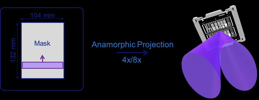
2021 EUVL Workshop

Presenting Author

Jan B.P. van Schoot, PhD, is Director of System Engineering and Technical
Specialist at ASML, based in Veldhoven, The Netherlands.

After his study Electrical Engineering (Cum Laude) at Twente University of
Technology. He received his PhD in Physics on the subject of non-linear
optical waveguide devices in 1994 and held a post-doc position studying
waveguide based electro-optical modulators.

He joined ASML in 1996 and was Project Leader for the Application of the first
5500/500 scanner and its successors up to 5500/750. In 2001 he became
Product Development Manager of Imaging Products (DoseMapper,
Customized Illumination). In 2007 he joined the dept of System Engineering.
He was responsible for the Optical Columns of the 0.25NA and 0.33NA EUV
systems. After this he worked on the design of the EUV source. He was the
study leader of the High-NA EUV system and is now responsible for the High-
NA optical train.

He is a Sr. Member of the SPIE, holds over 35 patents and presents
frequently at conferences about photolithography

www.euvlitho.com                                                                 8

2021 EUVL Workshop

P4

      Potential of EUV for High-volume Manufacturing of DRAM
                       (Keynote Presentation)

                                       Chang-Moon Lim

                                     SK hynix,
                    2091, Gyeongchung-daero, Bubal-eup, Icheon-si,
                              Gyeonggi-do, 17336, Korea

We are genuinely living in EUV HVM era, when several tens systems were shipped out a
year from an equipment maker and even larger number of them are under operation at
multiple places. That is mostly owing to the aggressive adoption by logic and foundry
industry, while introduction into memory sector lags little bit behind. Memory maker also
has been interested in development of this technology and has poured enormous effort to
utilize it for high volume manufacturing since long ago. In the presentation, briefly we will
review on what specific aspects has differentiated the memory sector from logic and
foundry in view of EUV adoption and will address about the current situation and potential
of EUV lithography for HVM of DRAM.

Presenting Author

Chang-Moon Lim has worked in various lithography technology
and process development for semiconductor memory
manufacturing for almost 30 years in SK hynix. He has lead the
development activity of EUV lithography in the company up to
now as a research fellow. He has published over 50 papers on
semiconductor lithography technology including EUV topics and
has given many presentations on various conferences. He has a
B.S. and Ph.D. in Physics from Seoul National University and
KAIST, respectively.

www.euvlitho.com                                                                        9
2021 EUVL Workshop

P5

                              EUV Lithography in
                   Volume Manufacturing and Future Extensions
                            (Keynote Presentation)

                                           Steve Carson

                                         Intel Corporation

Extreme Ultraviolet lithography equipment is maturing to a level that enables replacement
of 193nm-immersion as the leading-edge lithographic technology and simplifying complex
integrated process strategies. For EUV to be a successful replacement in high volume
manufacturing, the current successes of EUV technologies must be maintained, while the
challenges that remain need to be addressed. As always, the requirements for future nodes
drive increasingly aggressive targets that are creating new challenges for EUV technologies.
In this presentation, the status of EUV in high volume manufacturing will be reviewed. In
addition, the challenges for 0.33NA extension and 0.55NA insertion will be discussed.

Presenting Author

Steven L Carson is a Principal Engineer at Intel Corp. Steve joined the
Photolithography department in Intel’s Portland Technology Development
organization in 1999 after completing a B.S. degree at the California Institute
of Technology, and M.S. and Ph.D. degrees at the University of Florida, all in
Chemical Engineering. He has been involved with developing stepper and
scanner platforms from i-line to EUV for integration into high volume
manufacturing. He has also been involved in the development of advanced
process control (APC) applications and factory automation systems, earning
patents in both. Since 2008, Steve has primarily focused on EUV imaging
and its collateral technologies including the scanner, the source, EUV reticles,
and EUV pellicle membranes.

www.euvlitho.com                                                                       10
2021 EUVL Workshop
P11
EUV Masks: Prospects and Challenges (Invited)
Vicky Philipsen, Devesh Thakare, Joost Bekaert, Peter De Bisschop, Joern-Holger
Franke, Andreas Frommhold, Emily Gallagher, Rik Jonckheere, Tatiana Kovalevich,
Lieve Van Look, Vincent Wiaux, Eric Hendrickx
imec, Kapeldreef 75, B-3001 Leuven, Belgium
As the understanding of the EUVL grew, its different components – e.g., resist, scanner
optics, source - are being tailored to create the perfect aerial image and robust resist
pattern. Since recent years, the attention is moving more and more to the EUV mask. Mask
specific challenges involve mask deficiency induced stochastic failures, the anamorphicity of
high-NA EUVL and mask 3D effects. Pellicle development and mask lifetime understanding
are well progressing to control mask deficiency impact on wafer. Stitching enablement for
anamorphic imaging has been investigated leading to exclusion band recommendations.
Mask 3D effects, as a common denominator for inherent pitch- and orientation-dependent
wafer observations, are identified to limit wafer performance for current and future
technology nodes of 32nm pitch and below. Industry is also striving to increase the
throughput, but such a dose reduction can only be applied if the aerial image quality
allows.
Initial solutions to improve the aerial image are proposed by source-mask optimization,
where the illumination and mask design are compensating these wafer effects, which are in
fact due to the choice of the mask materials. Therefore, we have been studying different
mask concepts, including different materials, from lithographic perspective and
experimental mask material characteristics.
In this presentation, we will share our imaging insights in this imminent EUV-mask
technology change and highlight possible directions and challenges.
Presenting Author
Vicky Philipsen received her PhD degree in solid-state physics from the
University of Leuven (Belgium) in 2001. At imec she joined the Advanced
Patterning department, where her research domain involves the study of
mask 3D imaging effects in lithography (from 193nm to EUV and high NA
EUV) both by simulations and experiments. She is leading the project on
novel EUV mask absorbers at imec, including the technical task
responsibility in European projects.
www.euvlitho.com 112021 EUVL Workshop
P12
Comparison of Deposition Techniques for
Mo/Si Multilayers for EUV Mask Blanks (Invited)
Katrina Rook
Veeco Instruments, 1 Terminal Drive, Plainview NY 11803
Secondary ion beam deposition (IBD) is the process-of-record for deposition of Mo/Si
multilayers for the reflective coating of EUV mask blanks. IBD has been the method of
choice for at least 25 years, demonstrating outstanding performance for defectivity, central
wavelength control, and EUV-reflectivity.[1] As EUV transitions into high-volume
manufacturing, we assess the viability of alternative Mo/Si deposition techniques. Optical
calculations indicate that EUV reflectivity can be impacted by a few percent by: (a) Mo film
purity; (b) Mo/Si interfacial roughness and (c) Mo/Si interfacial intermixing. We present
film properties for single and multilayers deposited by IBD, DC magnetron sputtering, and
biased-target ion beam deposition. We compare film purity, microstructure, interlayer
roughness and interlayer intermixing. We present x-ray diffraction, x-ray reflectivity and x-
ray fluorescence; bright-field and dark-field TEM; and Rutherford Back-Scattering data.
Simulations can estimate the energetics of the depositing adatoms, and the resulting
interfacial properties. We have previously demonstrated good agreement between the
simulated results and TEM measurements.[2] Here we extend these simulations to estimate
theoretical limits on intermixing via the three deposition techniques.
[1] P. A. Kearney, C. E. Moore, S. I. Tan, S. P. Vernon, R. A. Levesque, Mask blanks for extreme ultraviolet lithography: Ion
beam sputter depostiion of low defect density Mo/Si multilayers, JVST B 15(6) (1997).
[2] Katrina Rook, Paul Turner, Narasimhan Srinivasan, Tania Henry, Kenji Yamamoto, Process optimization for performance
improvement in Mo/Si multilayers for EUV mask blanks, Proc. SPIE 11517 (October 2020).
Presenting Author
Dr. Katrina Rook is Applications Lab Manager with the Advanced
Deposition and Etch division of Veeco Instruments. Katrina has 30
years’ experience in the vacuum coating and etching of advanced
materials for applications in Data Storage, MEMS and Semiconductors.
She received her MS and PhD in Physics from Carnegie Mellon
University. For the past 4 years she has been engaged in Veeco’s EUV
program, in process development for mask-blank multilayer
deposition, and absorber deposition and ion beam etch.
www.euvlitho.com 122021 EUVL Workshop
P13
Efficient Modeling and Correction
of High-sigma EUV Stochastic Defects (Invited)
Zachary Levinsona, Yudhishthir Kandelb, Ryan Chenc, Yunqiang Zhangd, Rob
DeLanceyc, Makoto Miyagia, Kevin Lucasa
Synopsys Inc., 1301 S MoPac Expy Bld 4 # 200, Austin, TX 78746;
a
b
Synopsys Inc., 1101 Slater Road, Brighton Hall Suite 300, Durham, NC 27703
c
Synopsys Inc., 2025 NE Cornelius Pass Rd, Hillsboro, OR 97214
d
Synopsys Inc., 690 E Middlefield Rd., Mountain View, CA 94043
The quality of an optical lithographically transferred pattern is dependent on the uniformity
of photon absorption events that a photoresist pattern receives during exposure and the
uniformity of the subsequent molecular events in the photoresist. Process variation, and
subsequent control thereof, is not new to lithographers. For example, the resist film
thickness, the molecular weight of resist components, and hotplate temperatures all have
inherent variation. Additionally, photon statistics become increasingly important as the
photon count of the incident light decreases. The photon absorption event is the first in a
chain of stochastic processes in a lithographic process. These stochastic processes occur in
conjunction with conventional process variation. In extreme ultraviolet lithography (EUVL)
systems photon shot noise play a much larger role in image process development than in
DUV processes. This is due to a lower photon count which also increases the stochastic
variation of all the processes which occur after photon absorption. This causes the printed
edges of features across a chip to move away from the mean edge locations with some
probability that needs to be accounted for to ensure robust manufacturing.
Modern IC designs may fail if even 1 feature in 100M+ (7σ) is not patterned correctly on a
layer. Therefore, it is essential to EUVL patterning to detect and fix very rarely occurring
(e.g., high sigma) hotspots across the full chip. Full chip hotspot detection and repair
requires the use of fast modeling methods and for EUVL these models must incorporate
both stochastic and systematic effects in the process window. It is well-established in
lithographic literature that the CD distribution deviates from a normal distribution for very-
rare events beyond 3σ. The probability of failure due to stochastic variation in the
lithography process is not governed by the stochastics of any one physical or chemical
process. For example, a 7σ CD event is very unlikely to be solely caused by a 7σ event
from the photon distribution alone. Instead, the final process must be understood as being
dependent upon multiple stochastic events and conventional process variations that jointly
result in the observed final distribution of edge positions. There will also be multiple
probabilistic pathways that result in the same rare event. It is essential to EUVL process
development to be able to accurately predict and correct these very rarely occurring
events.
www.euvlitho.com 132021 EUVL Workshop A significant problem with building a model to predict high sigma (e.g., 7+ sigma) patterning failures is in gathering the reference experimental data which can show which pattern failures do occur but only with very small probability in a chip. Collecting 100M+ experimental datapoints is not a practical option. This presentation will examine ways in which a far smaller set of experimental datapoints can be used to train fast full-chip simulation model forms to predict and compensate for very rare EUVL patterning hotspots which occur due to a combination of systematic and stochastic variations. These model forms have previously been shown to be compatible with downstream correction tools (e.g. SMO, OPC, and/or ILT). Moreover, they have been shown to be able to predict and correct stochastic variation at a full-chip scale in realistic mask designs. Presenting Author Zac received his B.S, M.E, degrees in Microelectronic Engineering and his Ph.D. in Microsystems Engineering from the Rochester Institute of Technology where he studied under Dr. Bruce Smith. He has worked at Micron Technologies, TrueSense Imaging, and is currently employed as an Senior Application Engineer at Synopsys, Inc. He is author or co- author of >30 papers, including peer-reviewed articles and conference proceedings. His main research interests are EUV optics and stochastic variation in lithographic processes. www.euvlitho.com 14
2021 EUVL Workshop

P14

      Materials Perspectives for EUV Pellicle Solutions (Invited)

              Seong Ju Wi , Dongwook Kim , Kyeongjae Cho and Jinho Ahn
                              1                 2                   2           1

                        Division of Materials Science and Engineering
                          1

                     EUV-IUCC (Industry University Collaboration Center)
                     Hanyang University, Seoul, 04763, Republic of Korea

                      2
                       Department of Materials Science and Engineering,
                   University of Texas at Dallas, Richardson, TX 75080, USA

As the device manufacturers adopt EUV lithography in their production line, the control of
process yield and throughput has become an important issue for the profit maximization.
One of the key components which needs further improvements is the pellicle. A higher EUV
transmittance (>90%) is required to guarantee a higher throughput. Due to the continuous
demand on the source power upgrade, however, the thermal load on the pellicle will
continue to increase even with a high EUV transmittance. IR emission is the major cooling
mechanism of EUV pellicle due to membrane structure in a high vacuum environment. For
this point of view, we tried to find parameters affecting thermal stability/reliability of the
pellicle membrane. Experimentally we observed that IR emissivity shows linear dependency
on the resistivity, which can be increased by grain boundary scattering. And the particle
contamination on the pellicle surface induces localized thermal gradient (slower heating and
cooling due to a higher heat capacitance of the particle compared to the pellicle membrane)
can cause degraded reliability during repeated EUV scanning. Our study through thermo-
mechanical modeling and empirical observation will be introduced during the presentation.

Presenting Author

Jinho Ahn received his B.S. and M.S. degrees from Seoul National
University, and Ph.D. degree from the University of Texas at Austin all in
Materials Science and Engineering. He worked for Microelectronics
Research Laboratory at NEC, Tsukuba, Japan, and joined Hanyang
University in 1995 as a professor of Materials Science and Engineering. He
worked as a Director of Nano and Convergence Technology at National
Research Foundation of Korea, and the Vice President of Academic
Research at Hanyang University. Currently, he is the Director of EUV-
IUCC, which is funded by the member companies and partially supported
by the Korean government.

www.euvlitho.com                                                                         15
2021 EUVL Workshop
P15
Development of Advanced Blank Defect Avoidance
Technique using Actinic Review System (Invited)
Dong Gun Lee and Byung Gook Kim
ESOL (EUV Solution), Inc. 45, Dongtansandan 10-gil, Hwaseong-si, Gyeonggi-do,
Republic of Korea
With EUV lithography being applied to mass production of devices, blank supply for EUV
mask production is tight. Furthermore, securing an EUV blank with no defect is a significant
challenge in terms of cost and quantity. Therefore, applying a blank mask with as many
defects as possible to EUV mask production can bring many economic benefits. For this
reason, the blank defect avoidance technology [1], which shifts the pattern so that the
printed defect is minimized by using the position information of the blank defect and design
of the mask pattern in advance, is generally applied.
ESOL has developed an actinic defect review system called SREM [2] and is trying to apply
it to several EUV mask manufacturing processes. One of them is to improve the efficiency
of blank defect avoidance technique by reviewing the blank defect that has been inspected
by actinic blank inspection system. This addition of actinic review process can improve the
consistency of the algorithm for determining whether the transferability of defects in a
specific pattern by providing the same aerial image as the EUV scanner for blank defects,
along with accurate defect position information. Through this presentation, we will also
introduce phase measurement technology, an additional function of SREM that can be
automatically switched from one tool.
[1] Jihoon Na, Donggun Lee, Changhwan Do, Hong-seok Sim, Jung-Hwan Lee, Jungyoup Kim, Hwan-Seok Seo, Heebom Kim,
and Chan Uk Jeon, “Application of actinic mask review system for the preparation of HVM EUV lithography with defect free
mask,” BACUS Newsletter 33, Issue7 (2017).
[2] D. G. Lee, “Actinic Tools using Coherent EUV Source for High Volume Manufacturing,” EUVL Workshop (2020).
Presenting Author
Dong Gun Lee is the Chief Technology Officer of ESOL. He received an
M.S. and Ph.D. degree in Physics from the Korea Advanced Institute of
Science and Technology (KAIST). Prior to joining ESOL, he developed
tools for EUV mask production for the past 16 years as a Senior Principle
Engineer at the Samsung Electronics Semiconductor Research Institute.
www.euvlitho.com 162021 EUVL Workshop
P16
Evaluation Results of the Rapid Probe Microscope, RPM,
to Address EUV Mask 3D Metrology Requirements
M. Tedaldia, E. Gallagherb, A. Frommholdb, L. Fenga, A.D.L. Humphrisa, J. Gouldena
a
Infinitesima Ltd., Hitching Court, Abingdon OX14 1RG UK
b
IMEC, 3001 Leuven, Belgium
EUV lithography at 0.33 NA is entering high volume manufacturing. In parallel,
development activities are underway for EUV lithographic scanners with an NA of 0.55,
targeting resolution down to 8nm and extending Moore’s law into the next decade [1].
The mask is a critical part of the EUV imaging performance. The shorter wavelength and
increased angles of illumination associated with high NA imaging will enhance sensitivity to
mask surface roughness and variations in the mask absorber height. Additionally, low-
error OPC models require information on the mask absorber sidewall angles and profile of
different features. Finally, mask defect review can benefit from a complete profile and
roughness assessment before and after repairs.
The mask CD SEM is the tool of choice for 2D mask metrology but cannot provide accurate
data on the absorber height, sidewall angle or surface roughness. The Rapid Probe
Microscope (RPM) [2] is introduced as a solution for mask 3D metrology. The unique
technology of the RPM enables accurate 3D imaging in seconds, with a height
measurement capability of 0.5nm 3 sigma.
In this paper, several application cases will be presented to demonstrate the performance
of the RPM for mask metrology, examples of defect scans are shown in Figure 1 and 2.
Other potential use cases will also be explored, such as the surface roughness of the
multilayer mirror and the absorber layer and absorber height measurement.
Figure 1. Example RPM image of a programmed mask defect. Field of view is 2um. Absorber depth 70nm
www.euvlitho.com 172021 EUVL Workshop Figure 2. RPM image of contamination at the edge of the absorber. Contamination height approx. 55nm [1] Jan Van Schoot, Sjoerd Lok, Eelco van Setten, Ruben Maas, Kars Troost, Rudy Peeters, Jo Finders, Judon Stoeldraijer, Jos Benschop, Paul Graeupner, Peter Kuerz, and Winfried Kaiser "High-NA EUV lithography exposure tool: advantages and program progress", Proc. SPIE 11517 [2] Humphris et. al., ‘Probe microscopy for metrology of next generation devices’ Proc. SPIE 9778 Metrology, Inspection, and Process Control for Microlithography. 2016 Presenting Author Matthew Tedaldi has been working on advanced Scanning Probe Microscopy technologies for over 10 years. His career began in the National Physical Laboratory, the UK’s National Metrology Institute, developing the Metrological AFM to deliver traceable sub nanometre 3D measurements. Since joining Infinitesima in 2016, he has focused on the application and implementation of Infinitesima’s unique Rapid Probe Microscopy platform. As a Senior R&D Engineer his role is mostly dedicated to delivering quantifiable measurements in metrology and inspection in the semi-conductor industry. www.euvlitho.com 18
2021 EUVL Workshop

P17

                   Measuring In-pattern EUV Phase Deviations
                        with Linearized Scatterometry
      Stuart Sherwin[a], Ryan Miyakawa [b], Isvar Cordova[b], Markus Benk[b], Laura
                  Waller[a], Andrew Neureuther[a], Patrick Naulleau[b]

            [a]: UC Berkeley, Dept. of Electrical Engineering and Computer Science
                 [b]: Lawrence Berkeley National Lab, Center for X-Ray Optics

With the coming introduction of new EUV absorbers, there is an increasing need for actinic
phase metrology. One promising approach with demonstrated picometer sensitivity uses
reflectometry to determine the phase shift between the Fresnel reflection coefficients of
absorber and multilayer. One deficiency of this approach however is that the measurement
can only be carried out on a blank area of the photomask, and therefore could be blind to
in-pattern phase shifts that arise during mask fabrication or over the course of high-volume
manufacturing. Overcoming this hurdle requires an actinic measurement of light scattered
from a patterned region of the mask, where 3D scattering effects create substantial
computational difficulties relative to the Fresnel coefficient calculation used in
reflectometry. Here we propose a simplified solution for inferring deviations in these in-
pattern phase shifts by linearizing the relationship between scattered intensity and pattern
phase. Our proposed method requires measuring the scattered intensity from a periodic
target on the mask, computing the difference from a pre-defined nominal signal, and taking
a weighted sum of the deviation signal to estimate the phase. Both the nominal signal and
the weights are determined by rigorous electromagnetic simulation of a nominal mask
architecture as well as perturbations of geometric parameters.

Presenting Author

Stuart Sherwin received his Bachelor's in Physics and Applied Mathematics
from UC Berkeley in 2013. Following an interlude at KLA-Tencor in the
Reflective Electron Beam Lithography and 5D-Process Control teams, in
2016 he returned to UC Berkeley once again to pursue a PhD in Electrical
Engineering and Computer Science. Under the direction of Laura Waller,
Andy Neureuther, and Patrick Naulleau, his main research focuses are
Computational Imaging and EUV Lithography.

www.euvlitho.com                                                                       19
2021 EUVL Workshop
P18
EUV Phase-Sensitive Imaging Reflectometer
Yuka Esashi
STROBE Science and Technology Center, JILA, University of Colorado Boulder
Adoption of EUV lithography demands a parallel advance in metrology techniques with high
resolution and fidelity, in particular for actinic characterization of EUV masks. We present a
table-top phase-sensitive imaging reflectometer, which combines coherent diffractive
imaging with reflectometry to generate phase- and amplitude-reflectivity maps of a sample
at many incidence angles non-destructively. From the resulting angle-dependent reflectivity
map, the 3D composition of the sample can be solved in a spatially- and depth-resolved
manner. The microscope is illuminated by coherent EUV high harmonic beams, with
selectable wavelengths between 30 and 13.5 nm, allowing us to harness the high spatial
resolution and chemical specificity inherent to EUV light. Coherent diffractive imaging
measures the phase shift upon reflection in addition to the absolute reflectance, giving the
technique an enhanced sensitivity to material composition and surface topography, as well
as a unique ability to measure the phase of EUV masks with precision approaching 0.2
degrees. We have demonstrated this technique on a lithography test sample from imec,
where we were able to solve for various parameters of interest to the industry, including
layer thicknesses, structure heights, and dopant levels, which were verified using
correlative metrology [1].
[1] Tanksalvala et al., “Nondestructive, high-resolution, chemically specific 3D nanostructure characterization using phase-
sensitive EUV imaging reflectometry”, Science Advances, 7, 5, eabd9667 (2021).
Presenting Author
Esashi is pursuing her PhD in physics at the University of Colorado Boulder
in the Kapteyn–Murnane group. She is co-lead of the team implementing
the first table-top, ptychographic phase-sensitive imaging reflectometer
with EUV light, that can nondestructively image depth-dependent
composition of nanofabricated samples. Esashi received her BA in Physics
from Reed College in 2017, and her MS in Physics from the University of
Colorado Boulder in 2019.
www.euvlitho.com 202021 EUVL Workshop
P19
EUV Mask imaging Performance Enhancement
through Aerial Image Optimization
Deukgyu Kim , Dongmin Jeong , Yunsoo Kim ,
1, 3 2, 3 2, 3
Minsun Cho , and Jinho Ahn
1, 3 1, 2, 3
Division of Nanoscale Semiconductor Engineering
1
Division of Materials Science and Engineering
2
3
EUV-IUCC (Industry University Collaboration Center),
Hanyang University, Seoul, 04763, Republic of Korea
Extreme ultraviolet (EUV) lithography is in High volume manufacturing (HVM) for 7 nm
node and will continue expanding to future 5 nm node and beyond. But since there are
severe mask 3D effects such as non-telecentricity and best focus shift, the EUV mask still
struggles with mask contrast degradation.
In this work, we studied the optical property of the EUV absorber materials for the image
contrast optimization. We investigated the effects of phase and amplitude difference
between the 0th and 1st diffraction orders on the imaging performance in the range of low-
n (0.87 ≤ n ≤ 0.91) EUV mask absorbers. The simulation was performed for 14 nm half-
pitch line and space patterns with a leaf dipole off-axis illumination condition using KLA
Prolith 2020a simulation tool. We found that the image split, which means the difference in
distance between the aerial images formed from each pole, was reduced by using the
optimum phase difference between the 0th and 1st diffraction orders. In the case of 14 nm
HP L/S patterns, the optimum phase difference is 150 degrees. In addition, this result
becomes more clearly as the amplitude difference between the two diffraction orders
decreases.
As a result, it is possible to maximize mask image performance by optimizing the phase in
the low-n absorber range, where the amplitude difference between the two diffraction order
were minimized.
This research was supported by National R&D Program through the National Research Foundation of Korea(NRF) funded by
Ministry of Science and ICT(NRF-2020M3H4A3081881)
www.euvlitho.com 212021 EUVL Workshop Presenting Author Deukgyu Kim received his B.S. degree from Hanyang University in materials science and engineering, and he is studying EUV mask for next generation EUV lithography at Hanyang University as a master course of nanoscale semiconductor engineering. www.euvlitho.com 22
2021 EUVL Workshop

P20

                Applicability Verification for ZrSi based Pellicle                 2

                through Evaluating Optical/thermal Properties

                           Chang Soo Kim , Yong Ju Jang , Seong Ju Wi ,
                                                1,4                 2,4                                        3,4

                                  Ha Neul Kim , and Jinho Ahn
                                                      3,4                              1,2,3,4

                                Department of convergence nanoscience
                                   1

                       2
                           Division of Nanoscale Semiconductor Engineering
                             Division of Materials Science and Engineering
                               3

4

    EUV-IUCC (Industry University Collaboration Center), Hanyang University, Seoul,
                              04763, Republic of Korea

A high EUV transmittance and a low EUV reflectivity are must-have properties for the EUV
pellicles, but the compatibility with a high power EUV source is becoming a more important
issue. In this study, we investigated zirconium silicide (ZrSi ) material for the application of
                                                                                       2

EUV pellicle.

In order to fabricate ZrSi based pellicle, a silicon nitride (SiN ) membrane was fabricated
                                       2                                                           x

and then the ZrSi layer was deposited on the SiN membrane through co-sputtering
                           2                                              x

process. The EUV transmittance and reflectivity of ZrSi /SiN composite pellicle were       2           x

measured by EUV coherent scattering microscope (CSM). The thermal property evaluation
was performed using a heat load test equipment with UV laser having a 1:9 on/off
exposure ratio and high vacuum environment (
2021 EUVL Workshop Presenting Author Chang Soo Kim received his B.S. degree from Soongsil University in physics, and he is studying EUV pellicle for next generation EUV lithography at Hanyang University as a master course of convergence nanoscience. www.euvlitho.com 24
2021 EUVL Workshop

P21

              Synthesis of Organic-Inorganic Hybrid EUV Resists
                    by Atomic Layer Deposition (Invited)

                                       Chang-Yong Nam , Jiyoung Kim
                                                                1                   2

  1
      Center for Functional Nanomaterials, Brookhaven National Laboratory, Upton, NY
                                           11973
      Department of Materials Science and Engineering, University of Texas at Dallas,
      2

                                  Richardson, TX 75080

Hybrid photoresists containing inorganic elements offer high EUV absorption and etch
resistance. Optimizing resist exposure and patterning characteristics in hybrid resists
requires a facile control of the type and composition of incorporated inorganic elements, a
non-trivial task for the typical chemical synthesis. In this talk, I will discuss our recent
progress on synthesizing hybrid resists based on atomic layer deposition (ALD) and
preliminary EUV and low-energy electron exposure studies. Two distinctive approaches will
be presented, infiltration synthesis [1] and molecular ALD (MALD) [2]. The former utilizes
an infiltration of vapor-phase inorganic precursors into organic resists and the latter a
recursive layering of organic and inorganic molecular monolayers. Given facile
implementablility and ex-situ control of resist characteristics, the ALD-based hybrid resist
synthesis has a potential for enabling high-performance EUV resists.

[1]       N. Tiwale et al., Proc. SPIE 11612, Advances in Patterning Materials and Processes XXXVIII, 116120A (2021)
[2]       J. Huang et al., J. Mater. Chem. C. 4, 2382 (2016)

Presenting Author

Chang-Yong Nam is a Scientist at the Center for Functional Nanomaterials
(CFN) of Brookhaven National Laboratory (BNL). He is also an Adjunct
Professor of Materials Science and Chemical Engineering at Stony Brook
University. Chang-Yong received his Ph.D. in Materials Science and
Engineering from University of Pennsylvania (2007), M.S. in Materials
Science and Engineering from KAIST (2001), and B.E. in Metallurgical
Engineering from Korea University (1999; leave of absence for military
service during 1995 – 1997). Chang-Yong joined BNL in 2007 as a
Goldhaber Distinguished Fellow and has risen through the ranks to
Scientist in 2016. His current research addresses two focused areas: (a)
Development      and     application   of   ALD     techniques   toward
micro/nanoelectronics and energy technologies; (b) Materials processing
and device physics in organic semiconductors and low-dimensional
materials including nanowires and two-dimensional materials. His awards
include BNL Spotlight Awards (2018, 2011) and Goldhaber Distinguished
Fellowship (2007).

www.euvlitho.com                                                                                                       25
2021 EUVL Workshop
P22
Investigations of EUVL Photoresists
at the Advanced Light Source (Invited)
Luke Long,1 Terry McAfee,1 Patrick Naulleau,1 and Slavomír Nemšák2
1
Center for X-ray Optics, Lawrence Berkeley National Laboratory, Berkeley, CA 94720
2
Advanced Light Source, Lawrence Berkeley National Laboratory, Berkeley, CA 94720
At present, the success in the continuing miniaturization in the semiconductor industry
depends mostly on novel photolithographic techniques. In this work, we present the
experimental efforts focused on EUVL photoresists that are taking place at the Advanced
Light Source. The EUV radiation together with generated photoelectrons induce structural
and physio-chemical processes of the resists resulting in changes of their optical
properties.
X-ray photoemission spectroscopy (XPS) is a non-destructive technique that provides
information on the chemical and elemental composition of the photoresits as well as on any
present contaminants. In addition, when combined with standing-wave (SW) excitation, it
can provide non-destructive chemical and physical information of buried interfaces as well
as chemical and structural depth profile information with a few Angstrom resolution.
Another X-ray technique, Resonant Soft X-ray Scattering (RSoXS), probes the size scale
and distribution of aggregates within a photoresist by utilizing enhanced contrast provided
by chemical-bond specific contrast. RSoXS is typically limited to investigating features 1
nm or larger in size, but can probe sub-nm features using a line pattern approach.
G. Conti et al., Extreme Ultraviolet Lithography 115170I (2020); https://doi.org/10.1117/12.2575463.
Presenting Author
Slavomir Nemsak joined the Berkeley Lab as a postdoc in 2011 working in
the group of Prof. Fadley. In 2014 he became a group leader in
Forschungszentrum Juelich and was in charge of photoelectron microscopy
beamline at BESSY-II in Berlin. Since 2017 he is a staff scientist at the
Advanced Light Source working at soft and tender X-ray ambient pressure
photoemission beamlines.
www.euvlitho.com 262021 EUVL Workshop
P23
Exploring Backbone Ionization in EUV Resists
Using Computational Chemistry
Jonathan H. Ma
CXRO, Lawrence Berkeley National Laboratory, Berkeley, CA-94720, USA
Dept. of Physics, UC Berkeley, 366 LeConte Hall, Berkeley CA 94720, USA
The introduction of EUV lithography has triggered a new wave of material exploration.
There are a few challenges, including novel radiation chemistry and the Resolution-LER-
Sensitivity (RLS) trade-off. Innovative resist chemistry can lead to higher quantum
efficiency, which can help defeat the RLS trade-off. Mechanistic investigations are therefore
in the spotlight again.
Each EUV photon creates a cascade of secondary electrons which also leaves behind
multiple ionized resist molecules. On the one hand, the role of secondary electrons in
chemically amplified resists (CAR) has been extensively studied—they are shown to play a
major role in photo acid generator (PAG) activation. On the other, ionization chemistry
could provide extra leverage for dissolution chemistry.
Ionized species are short-lived and very unstable. While experimental studies exist, they
are made difficult by the transient nature of the reactive ionic species. Experimental efforts
can therefore be complemented by quantum chemistry computations, which provide a
preliminary understanding of ionization chemistry at a higher throughput, making it a
useful tool for identifying promising candidate materials.
We seek to understand the utility of this tool by studying relatively well-known systems
such as PMMA. Afterwards, we would proceed to investigate more novel idea such as the
inclusion of nitrogen into the polymer backbone. The inclusion of nitrogen can be used to
tune the ionization energy of the polymer. Its presence could however facilitate alternative
ionization chemistry. Quantum chemistry would therefore be a viable tool to understand the
interplay between the two.
www.euvlitho.com 272021 EUVL Workshop Presenting Author Jonathan H Ma is a graduate student from UC Berkeley. Working with Dr. Patrick Naulleau and Dr. Andrew Neureuther at the Center for X- ray Optics, his work focuses on understanding the novel radiation chemistry of EUV resists in various EUV material systems with both experiments and quantum chemistry computations. www.euvlitho.com 28
2021 EUVL Workshop

P24

      EUV Resist Development Program at NewSUBARU (Invited)

                   Takeo Watanabe, Shinji Yamakawa, Tetsuo Harada

                                      University of Hyogo

Extreme ultraviolet lithography is used in high volume manufacturing of 5-nm logic device
for the smart phones in 2020. IT technologies requires the semiconductor device which has
high operation frequency, low power consumption, and low production costs. Thus, more
advanced lithography is required.

NewSUBARU synchrotron light facility at University of Hyogo is the largest synchrotron
facility which is operated by the university in Japan. The main mission of this facility is
strong contribution to resolve the technology issues by the synchrotron industrial
applications.

In the development of EUV lithographic technology, the fundamental R&D has been carried
since 2000. The novel EUV resist development program and technologies will be
introduced.

Furthermore, our own electron beam injector is going to install for NewSUBARU
synchrotron electron beam storage ring. This linear accelerator (linac) is c-band accelerator
which has half length of the previous linac, and can accelerate the electron beam to 1.0
GeV.

Presenting Author

Takeo Watanabe received his Ph.D. from Osaka City University in 1990.
He is Full Professor, Director of Center for EUV, and Dean Laboratory of
Advanced Science and Technology for Industry, University of Hyogo. He is
an expert of the EUV lithographic technology, including optics, exposure
tool, mask and resist related technologies. He has authored over 200
technical papers, and he is international affair, and the organizing and
program committee members, of the International Conference of
Photopolymer Science and Technology (ICPST). He is also Conference
Chair of the International Conference of Photomask Japan. And he is a
program committee member of the International Conference on Electron,
Ion, and Photon Beam Technology and Nanofabrication (EIPBN).

www.euvlitho.com                                                                        29
2021 EUVL Workshop
P25
A Stochastic Resist Model Based Comparison
of 0.33NA and 0.55NA Lithography
Ruben Maas, Gijsbert Rispens, Eelco van Setten, John McNamara, Jan van Schoot
ASML, Veldhoven, The Netherlands
In this work, we introduce a 3D stochastic resist model developed to evaluate lithography
performance. We use the model to determine what dose-to-size, pattern variability and
stochastic defectivity to expect for several use-cases. Furthermore, the model is applied to
quantify the impact of resist properties such as film thickness, absorptivity, and blur on
pattern variability and defectivity. One key finding is that taking into account the 3D nature
of patterns is essential to predict stochastic defectivity. Furthermore, it is found that local
chemical variability within the resist has a significant contribution to the total pattern
variability.
Finally a model based comparison of 0.33NA and 0.55NA scanner performance is made in
terms of stochastic defectivity. A hexagonal pitch 28 nm contact hole pattern is studied as
a test use-case. This pattern can be printed with 0.33NA in a double exposure flow, or with
a single exposure using a 0.55NA scanner. The higher optical contrast of 0.55NA leads to a
larger defect-based exposure latitude, but comes at the cost of a limited defect-based
depth-of-focus. This work shows the need for careful pupil optimization to balance the peak
normalized image log slope with the depth-of-focus.
Presenting Author
Ruben Maas studied physics at Utrecht University and received his PhD in
nanophotonics from the University of Amsterdam in 2015, working on the
fabrication and characterization of optical metamaterials. Since then, he
has joined the Research department of ASML and works on stochastics in
EUV lithography and SEM metrology.
www.euvlitho.com 302021 EUVL Workshop
P26
A Decade of Progress in EUV resists (Invited)
Y. Ekinci
Paul Scherrer Institute, 5232 Villigen PSI, Switzerland
EUV lithography has become the leading lithography technique in semiconductor
manufacturing. Development of effective EUV resists was one of the key achievements that
enabled this success. Towards high-NA EUVL photoresists with better resolution and line-
edge roughness are needed. In this talk, I will review the advancements in EUV resists and
also the current status. I will also talk about the importance of metrology in assessment of
resist performance and about our efforts to improve this.
Presenting Author
Yasin Ekinci is head of the Laboratory of Micro and Nanotechnology at Paul
Scherrer Institute, Switzerland. He obtained his PhD in Max-Planck
Institute for Dynamics and Self-Organization, Göttingen, Germany in
2003. In 2004, he joined Paul Scherrer Institute as a postdoctoral
researcher. Between 2006 and 2012 he worked as a postdoctoral
researcher and subsequently as a senior scientist and a lecturer in
Department of Materials at ETH Zürich. He is at PSI since 2009 working
on various topics of nanoscience and technology, including EUV
lithography, resist materials, lensless imaging, plasmonics, semiconductor
nanostructures, and nanofluidics. He is author/co-author of more than 220
papers and 7 patent applications. He is a fellow of SPIE.
www.euvlitho.com 312021 EUVL Workshop
P27
EUV Lithography using Multi-Trigger Resist (Invited)
C. Popescu , G. O’Callaghan , A. McClelland , J. Roth , T Lada , T Kudo , M Moinpour ,
a a a b b c c
Y Cao , A.P.G. Robinson
c a,b
a
Irresistible Materials, Birmingham Research Park, Birmingham, UK
b
Nano-C, 33 Southwest Park, Westwood, MA, USA.
c
EMD Performance Materials Corp, Merck, USA
The development of novel EUV resists is widely agreed to be one of the highest priority
challenges for the deployment of high-NA EUV lithography. One potential approach is the
multi-trigger concept wherein a reaction will only occur when multiple elements of the
resist are initiated concurrently and in close spatial proximity. At the centre of exposed
features, where the exposure dose is sufficient the resist reaction is thus catalytic as in a
CAR, but at the edge of the features the reaction is second-order in nature, and thus the
chemical gradient is increased. In effect the resist features an intrinsic, inversely dose
dependent, quenching of the catalysis, enhancing the chemical contrast and thus
resolution, and reducing roughness.
The multi-trigger material consists of a novel MTR molecule and a crosslinker, which
represent the resist matrix, together with a photoacid generator (PAG). Research is
continuing to upgrade this resist, in particular focusing on improving resist opacity and
crosslinking density. A new high-Z crosslinker molecule has been synthesized and
formulated in the MTR resist. We report results obtained using this new MTR system
containing this cross-linker, with a variety of process conditions and formulation variations.
Furthermore, we have also investigated increasing the activation energy of the self-
quenching aspect of the MTR system.
Presenting Author
Alex Robinson is the co-founder and Chief Technical Officer of
Irresistible Materials, and a Senior Lecturer in the School of
Chemical Engineering at the University of Birmingham. He has over
twenty years of experience in research in to materials and
processes for nanofabrication, including the development of EUV
photoresists, and ultrahigh carbon content solution processed films
for high aspect ratio plasma etching. Other research interests
include the integration of top-down lithography with bottom-up
self-assembly of aptamer biosensing molecules for biodetectors,
novel nanostructured catalyst via synthetic biology approaches, and
investigations of ultra-high Stokes shift organic fluorescent
materials for bio-imaging applications.
www.euvlitho.com 322021 EUVL Workshop
P28
Exploration of Thin Films for High NA EUV Lithography
Joren Severi
KU Leuven, Celestijnenlaan 200F, B-3001, Leuven, Belgium
Imec, Kapeldreef 75, B-3001, Leuven, Belgium
The current advancement of EUV lithography (EUVL) is heavily based on the advancement
to the so-called high NA EUVL. At the same time, the film thickness that is used for resist
patterning must be reduced due to the expected reduced Depth-of-Focus (DoF) because of
the higher NA, as well as to prevent pattern collapse due to high aspect ratios for smaller
pitches. Reducing the film thickness leads to an expected more dominant interaction of
resist and underlayer which may lead to changes in material characteristics that could
affect the resist patterning performance, as well as metrology issues. To this end an
exploration of thin films was started at imec of which some results will be presented during
this talk.
Presenting Author
Joren Severi has received his Master of Chemistry degree from KU Leuven
in 2018, after which he started a PhD in Chemistry in the Exploratory
Patterning Materials (EPM) group at imec. The main topic of the thesis is
ultra-thin film characterization for high NA EUV lithography. The outcome
of the thesis should provide insight in both potential material changes,
changes in resist patterning performance, and ultimately design rules for
resists going to these ultra-thin films.
www.euvlitho.com 332021 EUVL Workshop
P29
Experimental Characterization of Model Polymers (Invited)
Oleg Kostko, Terry McAfee, Jonathan Ma, Patrick Naulleau
1,2 2 2,3 2
Chemical Sciences Division, Lawrence Berkeley National Laboratory, Berkeley, CA,
1
USA
Center for X-Ray Optics, Lawrence Berkeley National Laboratory, Berkeley, CA, USA
2
Department of Physics, University of California, Berkeley, CA, USA
3
The absorption of an EUV photon by a thin film resist leads to emission of primary and
secondary electrons. The electrons may travel up to tens of nanometers before losing their
kinetic energy via collisions which initiate chemical reactions. The “blur” of an aerial image
is directly related to the distance that electrons are able to travel in the resist. Thus,
identifying how to measure and influence the absorption of EUV photons, emission of
electrons, and distance traveled by the secondary electrons is extremely beneficial to the
resist community.
In this work, we utilize several model polymer materials to experimentally investigate the
impact of specific chemical groups on three critical resist properties: EUV absorption,
electron emission, and the electron attenuation length (EAL). EUV absorption dictates the
efficiency of the film to absorb photons. Total electron yield (TEY) provides information on
the conversion of absorbed EUV photons to electrons. The EAL corresponds to the thickness
of a material required to reduce the number of emitted electrons to 1/e of the initial value.
The EAL reveals the distance the electrons can travel in a resist film, which is directly
related to the electron blur. We will also discuss correlations between the obtained
experimental values.
Presenting Author
Oleg Kostko obtained his doctoral degree from the University of Freiburg,
Germany, in 2007. The same year he joined the Berkeley Lab as a
postdoctoral fellow. After a short stay at SRI International, where he
studied atmospherically relevant processes, he returned to the Berkeley
Lab to lead an effort for developing novel soft x-ray spectroscopies on
nanoscale systems. He also investigates fundamental processes in EUV
induced chemistry.
www.euvlitho.com 342021 EUVL Workshop
P30
Recent Progress in a Dry-deposited and Dry-developed
EUV Photoresist System (Invited)
Nader Shamma
Lam Research, 4650 Cushing Parkway, Fremont, CA 94538, U.S.A.
Extreme ultraviolet (EUV) lithography has been introduced into high volume manufacturing
(HVM) of semiconductor ICs beginning at the 7nm node logic and is being qualified for an
increasing proportion of lithography layers at 5/3nm logic and 16/14nm DRAM. A persistent
challenge of the EUV scanner is to supply a high contrast image with sufficient photons to
the photoresist to meet HVM productivity targets with acceptable dimensional and
defectivity control. Local stochastic variability dominates the total dimension control
budget and reducing that variability -by increasing the exposure dose- comes at the cost of
scanner throughput.
EUV scanner power and reliability have made significant improvements over the last decade
to HVM levels; however photoresists have not kept pace with the increasingly stringent
technology requirements during the same period. Spin-on photoresist materials are still
unable to meet the sensitivity, resolution, and defectivity targets for HVM of the most
advanced technology nodes. This gap in photoresist readiness has required IC fabs to make
compromises in design and cost and placed significant burden on downstream processes to
compensate for limitations in the lithography pattern, providing a significant opportunity for
innovation.
We discuss here our revolutionary technique to both apply photoresist and develop latent
images in photoresist using dry technologies instead of the existing wet spin coating and
development that have been in use for over 40 years. We will review the key advantages of
dry resist processing over wet resist processing: stability, photosensitivity, environmental
footprint, process window, and cost. This nascent technology has demonstrated best-in-
class photoresist performance at leading edge design rules and enables a new world of
innovations in EUV lithography patterning.
Presenting Author
Nader Shamma is currently serving as Technical Director at Lam Research
Office of CTO. He has contributed to the development of several
generations of lithographic processes for advanced semiconductor IC
fabrication.
www.euvlitho.com 352021 EUVL Workshop
P31
EUV Resists: Pushing the Limits (Invited)
Anna Lio
Intel Corporation
Extreme Ultraviolet Lithography (EUVL) has become mainstream. Its continued success is
strongly dependent on pushing EUV photoresists to their limits. We discuss status of EUV
photoresist development and asks of the entire EUV ecosystem to enhance and accelerate
EUV resist development.
Presenting Author
Dr. Anna Lio is a Senior Principal Engineer at Intel Corporation, Portland
Technology Development. She manages the development of all EUV
lithography materials for Intel’s current and next generation technologies.
Prior to that she led the development of lithography processes for Intel’s
revolutionary trigate transistor process technology at the 22 nm node.
She joined Intel in 1997 and has worked in the area of photoresist, design
rules definition, microprocessor process development and integration for
every Intel’s technology starting at the 130nm node. Anna holds a M.S. in
Physics from the University of Pisa (Italy) and a PhD in Electrical
Engineering from the University of Glasgow (UK). During her PhD, she
was a visiting scholar at the Materials Sciences Division at LBNL in
Berkeley, CA – an experience that ultimately shaped her personal and
professional life. Anna is passionate about empowering women in science
and engineering and is an active mentor at the corporate, college and
high school level.
www.euvlitho.com 36You can also read