AN12365 NTAG 5 - How to use energy harvesting Rev. 1.2 - 18 May 2020 530412 - NXP Semiconductors
←
→
Page content transcription
If your browser does not render page correctly, please read the page content below
AN12365
  NTAG 5 - How to use energy harvesting
  Rev. 1.2 — 18 May 2020                                              Application note
  530412                                                            COMPANY PUBLIC

Document information
Information     Content
Keywords        NTAG 5 switch, NTAG 5 link, NTAG 5 boost, energy harvesting, circuit,
                schematics, reference application
Abstract        Guidelines for designing applications using NTAG 5 energy harvesting
                capabilities.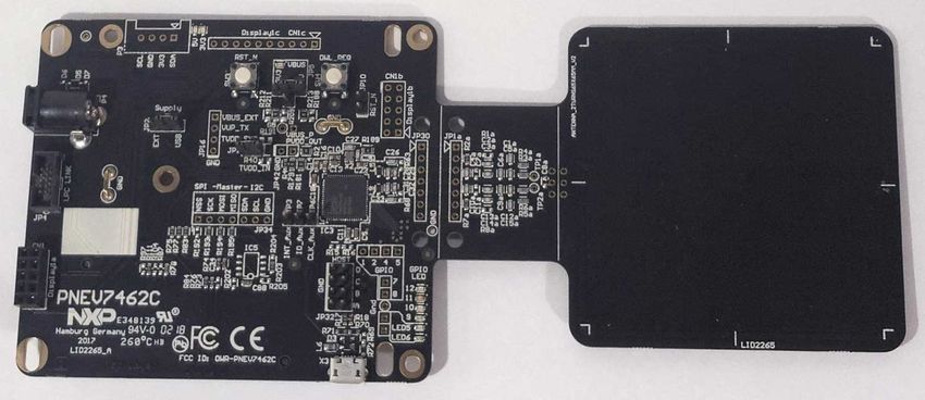
NXP Semiconductors
                                                                                                                     AN12365
                                                                                                 NTAG 5 - How to use energy harvesting

Revision history
Rev           Date       Description
v.1.2         20200518   Updates on modes of operation, EH block, see Section 3.3 and Section 2.3, Figure 3
                         updated
v.1.1         20200304   General update
v.1.0         20200109   Initial version

AN12365                         All information provided in this document is subject to legal disclaimers.           © NXP B.V. 2020. All rights reserved.

Application note                                Rev. 1.2 — 18 May 2020
COMPANY PUBLIC                                          530412                                                                                   2 / 25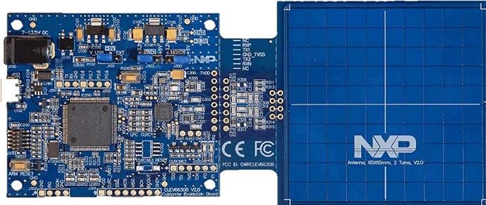
NXP Semiconductors
                                                                                                                        AN12365
                                                                                                    NTAG 5 - How to use energy harvesting

1         Abbreviations
                    Table 1. Abbreviations
                    Acronym           Description
                    NFC               Near Field Communication
                    EH                Energy Harvesting
                    ALM               Active Load Modulation
                    VCD               Vicinity Coupling Device
                    VICC              Vicinity Integrated Circuit Card

AN12365                            All information provided in this document is subject to legal disclaimers.           © NXP B.V. 2020. All rights reserved.

Application note                                   Rev. 1.2 — 18 May 2020
COMPANY PUBLIC                                             530412                                                                                   3 / 25
NXP Semiconductors
                                                                                                                            AN12365
                                                                                                        NTAG 5 - How to use energy harvesting

2         Introduction
                       This document describes "energy harvesting" capabilities of NTAG 5 family ICs. NTAG
                       5 phrase in this document refers to all three IC variants: NTAG 5 switch, NTAG 5 link,
                       NTAG 5 boost. To reduce complexity, NTAG 5 abbreviation is used through whole
                       document for all three IC variants.
                       The NTAG 5 provides the capability to harvest energy from the RF field. This feature
                       can be used to supply external circuits or devices (e.g., microcontrollers, sensors) with
                       enough energy to operate.

                       NTAG 5 is the first IC with configurable regulated power output.

                       This document focuses on showing how much energy the NTAG 5 can deliver and under
                       which conditions, how to design a circuitry to optimize energy harvesting capabilities.
                       It shall be considered that ALM (Active Load Modulation) functionality and energy
                       harvesting are not available at the same time.

                        Figure 1. Harvesting ambient RF energy with NTAG 5 - concept

                       In the case energy harvesting is used to power NTAG 5 (when VCC is not supplied
                       externally), all harvested excess power (power not required to supply NTAG 5) is
                       available to supply external circuits.

                       NTAG 5 consists of configurable current detection block. It allows triggering energy
                       harvesting only when enough energy is retrieved from RF to provide expected current
                       level.

                   2.1 Target applications
                       • Fully sealed devices
                                                                    2
                       • Sensor Tags, Sensor tags with NTAG 5 in I C master mode (w/o MCU), reference
                         [Application note]
                       • Maintenance of broken systems, in case of general power outage, reference
                         [Application note]
                       • Especially for devices where power is an issue

                   2.2 Influencing factors on energy harvesting
                       Main factors influence the power NTAG 5 is able to harvest are the following:
                       • Antenna size: Larger is the NTAG 5 antenna higher is the level of energy collected by
                         NTAG 5 from RF.

AN12365                                All information provided in this document is subject to legal disclaimers.           © NXP B.V. 2020. All rights reserved.

Application note                                       Rev. 1.2 — 18 May 2020
COMPANY PUBLIC                                                 530412                                                                                   4 / 25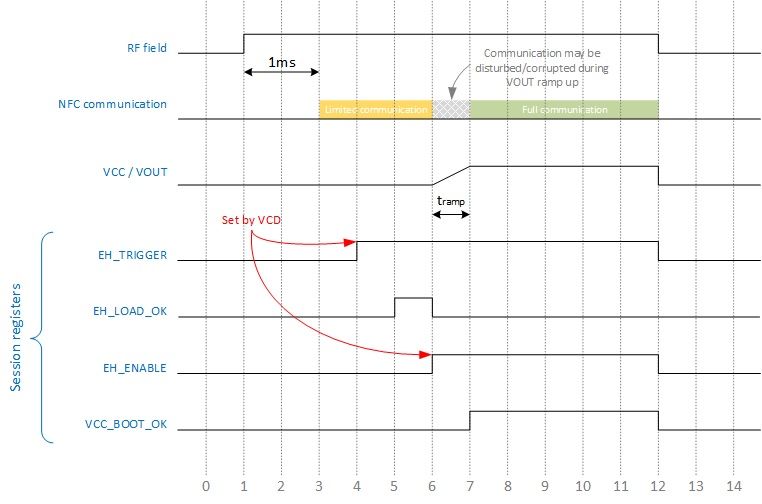
NXP Semiconductors
                                                                                                                                      AN12365
                                                                                                        NTAG 5 - How to use energy harvesting

                        • Antenna turn count: Lower is the number of turns higher is the level of energy collected
                          by NTAG 5 from RF.
                        • Antenna matching: In case of highly coupled systems (reader and NTAG 5 antennas
                          size are the same, with small or even zero distance in between) the reader can be
                          detuned from the tag. This can reduce amount of energy collected by NTAG 5.
                        • Field strength: Stronger is the field emitted by the RF reader higher is the level of
                          energy collected by NTAG 5. Field strength dropping while distance between reader
                          antenna and NTAG 5 antenna increase.

                        Note: In general, under the load VOUT voltage drops if too much current is taken
                        out of the NTAG 5 or if field strength gets weaker. In this condition (DISABLE_
                        POWER_CHECK = 0b and field strength too weak to deliver configured output) NTAG
                        5 only responds to INVENTORY command and READ/WRITE CONFIGURATION to
                        access session registers on NFC interface side.
                                   2
                        For stable I C communication, the VCC should not drop below recommended minimum
                        VCC (Electrical characteristics in [Datasheet]).

                   2.3 Modes of operation
                        There are two (2) modes which can be set for energy harvesting operation, with bits
                        EH_MODE:
                        • Energy harvesting optimized for low field strength (default) - if expected VCDs have
                          lower NFC field strength (e.g. NFC mobiles). The low field strength mode is optimized
                          for high energy harvesting efficiency and can drive up to 20 mW output power.
                        • Energy harvesting optimized for high field strength - if expected VCDs be able to output
                          more strong field (e.g. specially designed VCDs). The high field strength mode can
                          drive higher power and also supports a VCD with 10 % modulation index next to the
                          100 % ASK modulation scheme.

Table 2. Modes of EH operation comparison
                                       Low Field Strength                                                           High Field Strength
Energy harvesting efficiency           Best                                                                         10 % - 20 % reduced efficiency vs Low
                                                                                                                    Field Strength Mode
Energy harvesting power                < 20 mW                                                                      > 20 mW (< 50 mW)
Modulation scheme                      100 % ASK VCD Modulation                                                     10 % and 100 % ASK VCD Modulation

AN12365                                All information provided in this document is subject to legal disclaimers.                      © NXP B.V. 2020. All rights reserved.

Application note                                       Rev. 1.2 — 18 May 2020
COMPANY PUBLIC                                                 530412                                                                                              5 / 25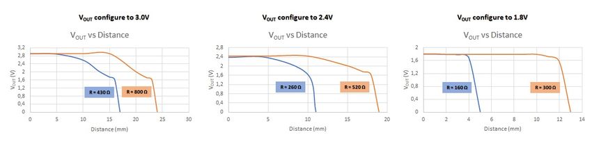
NXP Semiconductors
                                                                                                                               AN12365
                                                                                                           NTAG 5 - How to use energy harvesting

 Figure 2. Current vs. Load vs. H field

AN12365                                   All information provided in this document is subject to legal disclaimers.           © NXP B.V. 2020. All rights reserved.

Application note                                          Rev. 1.2 — 18 May 2020
COMPANY PUBLIC                                                    530412                                                                                   6 / 25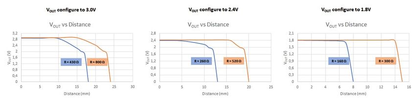
NXP Semiconductors
                                                                                                                                 AN12365
                                                                                                        NTAG 5 - How to use energy harvesting

3         Recommendations
                       To optimize energy harvesting as whole, following topics shall be considered: on system
                       level and on components surrounding IC.

                   3.1 System level
                       • Minimize the current needed to be harvested. Energy supplied via EH, needs to be
                         supplied by the reader, therefore reduces the read range of the NTAG 5.
                       • On MCU systems, clock down the MCU and also use the deep sleep modes to
                         minimize the current consumption.
                       • The power requirements connected to the energy harvesting pin should be kept at
                         minimum as needed by the external system. The larger the requirements are, the
                         harder it is for the reader to wake up and supply the NTAG 5.
                       • Use optimum Vtx level on VCD

                   3.2 Application level
                       The external capacitor (C below) value must be chosen to prevent voltage drop below
                       100 mV during VCD modulation pauses.

                                                            LA

                                             C1
                                                                                                                    VCC
                                                                                  NTAG 5
                                                                                                                     VOUT
                                                            LB                                                                        RLOAD
                                                                                                                            C2

                                                                                                                    GND

                        Figure 3. Example application circuit

                       Voltage drop during VCD pauses (miller modulation type) can be calculated following
                       below formula, where Vdrop is the voltage drop during VCD modulation pauses in volts, IL
                       is the load current in amps and tpause is the modulation pause duration in seconds:

                                                                                                                                                              (1)

AN12365                                All information provided in this document is subject to legal disclaimers.                © NXP B.V. 2020. All rights reserved.

Application note                                       Rev. 1.2 — 18 May 2020
COMPANY PUBLIC                                                 530412                                                                                        7 / 25
NXP Semiconductors
                                                                                                                                        AN12365
                                                                                                          NTAG 5 - How to use energy harvesting

                       Additionally, the external capacitor value impacts the VOUT ramp-up time according below
                       formula, where tramp is the VOUT ramp-up time in seconds and Ifield is the configured
                       output current in amps (refers to EH_VOUT_I_SEL):

                                                                                                                                                                      (2)

                                                                                                                                                      1
                       • VOUT can also be used as an "NFC field detector" alternative (among ED pin )
                                                                                     2
                       • In case NTAG 5's VOUT (harvested energy) also supplies I C bus, then VCC must be
                         connected to VOUT, and pull-up resistors are required on the SCL and SDA lines.
                         These pull-up resistors must be sized appropriately to limit the sink current when the
                         lines are pulled low. Resistors value depends on the devices connected on the bus,
                         recommendation is to start with value 4.7 kOhms and adjust it down if necessary.
                       • In case NTAG 5's VOUT (harvested energy) also supplies ED pin (Event Detect pin
                         [Application note]) in Pass-through mode [Application note], then the pull-up resistor on
                         the Event Detect line must be sized appropriately to limit the sink current when pulled
                         low by NTAG 5.
                       1
                           When using ED pin functionality, NTAG 5 does not need to be VCC supplied.

                   3.3 Energy harvesting block operation
                       NTAG 5 includes a power check block, which offers a current detection mechanism and
                       can be enabled or disabled through DISABLE_POWER_CHECK. Current detection
                       mechanism will be operating (if enabled) ONLY when RF field is available. The current
                       detection mechanism compares harvested current with a reference value and enables
                       the output Vout only, when the harvested current is higher than the reference value.
                       Note: If the current detection is enabled and there is not enough field strength available
                       to enable VOUT, EEPROM access is disabled. NTAG 5 is then answering ONLY to
                       INVENTORY command and READ/WRITE CONFIGURATION to access session
                       registers on NFC interface.

                       The block „energy harvesting“ can operate in low or high field strength mode
                       (Section 2.3) and it includes a shunt regulator which provides the configured regulated
                       voltage (EH_VOUT_V_SEL) at Vout.

                                                                                                                                  VCC
                                                                EH_VOUT_V_SEL
                                                                EH_MODE
                                          LA                    DISABLE_POWER_CHECK
                                                                                                                                  VOUT
                                                                                                           energy
                                    C1
                                                                                                          harvesting
                                                        rectifier
                                                                                  power                                                        C2             RLOAD
                                                                                  check                               EH_ENABLE

                                          LB
                                                                EH_TRIGGER
                                                                EH_VOUT_I_SEL
                                                                EH_LOAD_OK

                        Figure 4. NTAG 5's energy harvesting block diagram

AN12365                                  All information provided in this document is subject to legal disclaimers.                     © NXP B.V. 2020. All rights reserved.

Application note                                         Rev. 1.2 — 18 May 2020
COMPANY PUBLIC                                                   530412                                                                                             8 / 25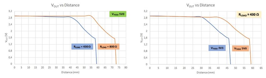
NXP Semiconductors
                                                                                                                       AN12365
                                                                                                   NTAG 5 - How to use energy harvesting

                   EH_LOAD_OK is a bit in session register that indicates if sufficient energy, harvested
                   from RF, is available.

AN12365                           All information provided in this document is subject to legal disclaimers.           © NXP B.V. 2020. All rights reserved.

Application note                                  Rev. 1.2 — 18 May 2020
COMPANY PUBLIC                                            530412                                                                                   9 / 25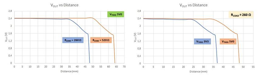
NXP Semiconductors
                                                                                                                             AN12365
                                                                                                         NTAG 5 - How to use energy harvesting

4         How to configure NTAG 5 for energy harvesting
                       Mode of energy harvesting feature can be configured by either of following bytes:
                                                                                                                                           2
                       • EH_CONFIG_REG in session register (Block address from NFC:A7h, from I C:10A7h,
                         Byte0) >> Current session
                                                                                              2
                       • EH_CONFIG in configuration memory (Block address from NFC:3Dh, from I C:103Dh,
                         Byte0) >> Start-up behavior

                       As soon as energy harvesting is used, VOUT and VCC must be connected. Otherwise
                       no EEPROM access is possible from NFC side and status registers reflect invalid
                       information.

                       Detailed description of those parameters can be found in NTAG 5 [Datasheet].

                       The two different possible methods of enabling EH are described in next chapters:
                       1. Enabling EH by session registers (Recommended method) [Section 4.1]
                       2. EH enabled during boot [Section 4.2]

                   4.1 Enabling EH by session registers - the recommended method
                       This first method is the recommended one because it provides more reliable NFC
                       communication (less time slot in which NFC communication cannot be fully achieved).
                       However it requires dedicated scenario from the VCD side, therefore requiring specific
                       application running on VCD.
                       Prerequisites:
                                                                                                            2
                       • in EH_CONFIG (3Dh from NFC / 103Dh from I C):
                         – Energy harvesting at startup must be disabled, setting bit EH_ENABLE to 0b, since it
                           will on the fly be enable through session register
                         – EH_VOUT_V_SEL and EH_VOUT_I_SEL must be set according to the requirement
                         – DISABLE_POWER_CHECK has no effect, as EH_ENABLE is set to 0b
                                                                    2
                       • In CONFIG (37h from NFC / 1037h from I C) desired energy harvesting mode must be
                         chosen (optimized for low or high field strength - see Section 2.3)
                       Procedure:
                       1. VCD triggers current detection by by writing to EH_CONFIG_REG session register
                          (A7h) → EH_TRIGGER (Bit3) set to 1b
                       2. VCD polls EH_CONFIG_REG (A7h) until the available field strength is sufficient →
                          EH_LOAD_OK (Bit7) equal to 1b
                       3. VCD enables the energy harvesting by writing to EH_CONFIG_REG session register
                          (A7h) → EH_ENABLE (Bit0) set to 1b and EH_TRIGGER (Bit3) set to 1b
                       4. VCD polls STATUS1_REG (A0h) until VCC ramps up → VCC_BOOT_OK (Bit7) equal
                          to 1b

                       Note: If VCD directly enables EH (step 3) without checking if field strength is sufficient
                       (step 1 and 2), risk is NTAG 5 may reset because of voltage drop (if not enough energy).
                       EH will be disabled (since only valid for current NFC session).
                                                                                                                                                         2
                       Note: If EH_ARBITER_MODE_EN (CONFIG_1 register 37h from NFC / 1037h from I C)
                       is set to 0 the ARBITER_MODE is selected via CONFIG_1_REG session register (A1h
                       from NFC) since related setting from CONFIG_1 configuration register is ineffective.
AN12365                                 All information provided in this document is subject to legal disclaimers.           © NXP B.V. 2020. All rights reserved.

Application note                                        Rev. 1.2 — 18 May 2020
COMPANY PUBLIC                                                  530412                                                                                 10 / 25
NXP Semiconductors
AN12365
NTAG 5 - How to use energy harvesting
Limitations:
• Until VOUT gets generated and VCC ramps up, the communication to memory is not
possible. Only INVENTORY command and access to session registers are possible
from NFC interface.
• Any NFC communication during VOUT ramp up may be disturbed/corrupted.
Figure 5. Enabling EH by session registers time state diagram
Timestamp Description
1 RF field appears
3 NTAG 5 is ready for NFC activation from VCD
4 VCD writes to session register: EH_TRIGGER = 1b
4-5 VCD polls for EH_LOAD_OK status signal in session registers
6 VCD writes to session register EH_ENABLE = 1b and EH_TRIGGER = 1b
VCC boot starts. VCC boot to be restarted if VCC toggles between time 6 and 7
2
7 NFC and I C fully functional
7-12 If the RF field strength drops or Load current increases, the VOUT will drop, consequently also VCC drops
If VCC goes below 1.62 V, the system reset will be triggered and NTAG 5 will reboot
12 RF field disappears leading to VOUT drop then NTAG 5 shutdown
Note: Writing to Session Registers to enable energy harvesting, will be treated as a
"Write alike" command which means VCC ramp can go up to 20 ms max. If VCC supply
does not come up until 20 ms, then the VCD needs to take a corrective action.
AN12365 All information provided in this document is subject to legal disclaimers. © NXP B.V. 2020. All rights reserved.
Application note Rev. 1.2 — 18 May 2020
COMPANY PUBLIC 530412 11 / 25NXP Semiconductors
AN12365
NTAG 5 - How to use energy harvesting
4.2 Energy harvesting enabled during boot
This second method is the only one which can be considered if there is no control to the
VCD application.
Prerequisites
2
• in EH_CONFIG (3Dh from NFC / 103Dh from I C):
– Energy harvesting at startup must be enabled, setting bit EH_ENABLE to 1b
– EH_VOUT_V_SEL and EH_VOUT_I_SEL must be set according to the requirement
– DISABLE_POWER_CHECK can be configured to use current detection monitor or
not
Procedure:
• Depending on DISABLE_POWER_CHECK setting, energy harvesting will be directly
enabled after boot or only when field strength becomes stronger enough to generate
the required load
Limitations:
• Until VOUT gets generated and VCC ramps up, the communication to EEPROM is not
possible. Only INVENTORY command and access to registers are possible from NFC
interface.
• Any NFC communication during VOUT ramp up may be disturbed/corrupted.
Figure 6. EH enabled by Configuration Bytes timing state diagram
Timestamp Description
1 RF field appears
3 NTAG 5 is ready for NFC activation from VCD
3-6 VCD can activate NTAG 5 but cannot access memory (only access to registers is granted)
6 VCC boot starts. VCC boot to be restarted if VCC toggles between time 6 and 7
2
7 NFC and I C fully functional
7-12 If the RF field strength drops or Load current increases, the VOUT will drop, consequently also VCC drops
If VCC goes below 1.62 V, the system reset will be triggered and NTAG 5 will reboot
AN12365 All information provided in this document is subject to legal disclaimers. © NXP B.V. 2020. All rights reserved.
Application note Rev. 1.2 — 18 May 2020
COMPANY PUBLIC 530412 12 / 25NXP Semiconductors
AN12365
NTAG 5 - How to use energy harvesting
Timestamp Description
12 RF field disappears leading to VOUT drop then NTAG 5 shutdown
The EH sequence will be retriggered after every boot.
Time between RF field appears and VCC boot starts (timestamp 1 to timestamp 6) when
EH is enabled at boot, indicated as t1 on above diagram, is about 1.52 ms.
To check, if the NTAG 5 is powered and if EH is enabled or not, session register can be
checked:
2
• STATUS0_REG (A0h from NFC / 10A0h from I C), bit VCC_SUPPLY_OK
2
• EH_CONFIG (A7h from NFC / 10A7h from I C), bit EH_ENABLE
AN12365 All information provided in this document is subject to legal disclaimers. © NXP B.V. 2020. All rights reserved.
Application note Rev. 1.2 — 18 May 2020
COMPANY PUBLIC 530412 13 / 25NXP Semiconductors
AN12365
NTAG 5 - How to use energy harvesting
5 Antenna design guidelines
Optimal energy transfer can be achieved by considering the following recommendations:
1. larger antenna size with lesser turns
2. antenna size close to a reader's antenna size (but not exact same size to avoid
decoupling effect at low or zero distance)
To achieve most optimum configuration for RF performance (read range) and energy
harvesting power yield, it is recommended to use a parallel capacitor for tuning and to
lower antenna's inductance.
Example: For an antenna having total 1 µH inductance, parallel 82 pF tuning can be
used.
More details on "How to design antenna for NTAG 5" can be found in [Application note].
AN12365 All information provided in this document is subject to legal disclaimers. © NXP B.V. 2020. All rights reserved.
Application note Rev. 1.2 — 18 May 2020
COMPANY PUBLIC 530412 14 / 25NXP Semiconductors
AN12365
NTAG 5 - How to use energy harvesting
6 Example measurements
6.1 Reference setup
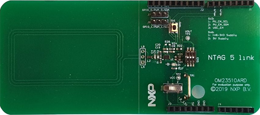
The reference setup used for the measurement is the NTAG 5 demo board referenced as
OM23510ARD featuring a 3 turns 54 mm x 27 mm antenna.
Figure 7. OM23510ARD NTAG 5 demo board
Following measurements are done using different devices, acting as Vicinity readers, to
provide wide range of NTAG 5 energy harvesting capabilities.
Note: Minimum load allowing to run energy harvesting depends on the VOUT
configuration:
• for VOUT configured to 3.0 V → minimum load is 430 Ω
• for VOUT configured to 2.4 V → minimum load is 260 Ω
• for VOUT configured to 1.8 V → minimum load is 160 Ω
6.1.1 CLRC663 plus demo board
Measurement with CLRC663 plus are performed using CLEV6630B demo board.
Figure 8. CLEV6630B CLRC663 plus demo board
AN12365 All information provided in this document is subject to legal disclaimers. © NXP B.V. 2020. All rights reserved.
Application note Rev. 1.2 — 18 May 2020
COMPANY PUBLIC 530412 15 / 25NXP Semiconductors
AN12365
NTAG 5 - How to use energy harvesting
See in below block diagram of the measurement setup.
Figure 9. CLRC663 plus measurement setup
Below are measurement results for different values of Rload and VTVDD, and different
VOUT configurations (EH_VOUT_V_SEL parameter).
Note: Measurements with CLRC663 plus are done with NTAG 5 set in energy harvesting
mode optimized for high field strength (EH_MODE parameter).
Figure 10. CLRC663 plus measurement results with VOUT configured to 3.0 V
Figure 11. CLRC663 plus measurement results with VOUT configured to 2.4 V
Figure 12. CLRC663 plus measurement results with VOUT configured to 1.8 V
AN12365 All information provided in this document is subject to legal disclaimers. © NXP B.V. 2020. All rights reserved.
Application note Rev. 1.2 — 18 May 2020
COMPANY PUBLIC 530412 16 / 25NXP Semiconductors
AN12365
NTAG 5 - How to use energy harvesting
6.1.2 PN7462 demo board
Measurement with PN7462 is performed using PNEV7462C demo board.
Figure 13. PNEV7462C PN7462 demo board
See in below block diagram of the measurement setup.
Figure 14. PN7462 measurement setup
Below are measurement results for different values of Rload and VTVDD, and different
VOUT configurations (EH_VOUT_V_SEL parameter).
Note: Measurements with PN7462 are done with NTAG 5 set in energy harvesting mode
optimized for high field strength (EH_MODE parameter).
Figure 15. PN7462 measurement results with VOUT configured to 3.0 V
AN12365 All information provided in this document is subject to legal disclaimers. © NXP B.V. 2020. All rights reserved.
Application note Rev. 1.2 — 18 May 2020
COMPANY PUBLIC 530412 17 / 25NXP Semiconductors
AN12365
NTAG 5 - How to use energy harvesting
Figure 16. PN7462 measurement results with VOUT configured to 2.4 V
Figure 17. PN7462 measurement results with VOUT configured to 1.8 V
6.1.3 NFC mobile phones
Measurement with mobile phones is performed using NFC mobile phones Google Pixel
3, Huawei P20 Pro and Apple iPhone 11.
Figure 18. NFC Mobile phones
See in below block diagram of the measurement setup.
AN12365 All information provided in this document is subject to legal disclaimers. © NXP B.V. 2020. All rights reserved.
Application note Rev. 1.2 — 18 May 2020
COMPANY PUBLIC 530412 18 / 25NXP Semiconductors
AN12365
NTAG 5 - How to use energy harvesting
Figure 19. NFC mobile phones measurement setup
Below are measurement results for different values of Rload and different VOUT
configurations (EH_VOUT_V_SEL parameter).
Note: Measurements with NFC mobile phones are done with NTAG 5 set in energy
harvesting mode optimized for low field strength (EH_MODE parameter).
Figure 20. Google Pixel 3 NFC mobile phone measurement results
Figure 21. Huawei P20 Pro NFC mobile phone measurement results
Figure 22. Apple iPhone 11 NFC mobile phone measurement results
AN12365 All information provided in this document is subject to legal disclaimers. © NXP B.V. 2020. All rights reserved.
Application note Rev. 1.2 — 18 May 2020
COMPANY PUBLIC 530412 19 / 25NXP Semiconductors
AN12365
NTAG 5 - How to use energy harvesting
6.2 Boot sequence example timings
Below is a diagram of a boot sequence example when EH is enabled by configuration
registers (see Section 4.2).
It shows timing of RF field ON event and VOUT signal ramp-up, until the start of a PWM
(GPIO_PAD1 configured as PWM output).
Figure 23. Enable EH by Config. bytes (Boot up behavior) - time/state diagram scope trace
AN12365 All information provided in this document is subject to legal disclaimers. © NXP B.V. 2020. All rights reserved.
Application note Rev. 1.2 — 18 May 2020
COMPANY PUBLIC 530412 20 / 25NXP Semiconductors
AN12365
NTAG 5 - How to use energy harvesting
7 References
[1] NTP5210 - NTAG 5 switch, NFC Forum-compliant PWM and GPIO bridge, doc.no.
5477xx
https://www.nxp.com/docs/en/data-sheet/NTP5210.pdf
2
[2] NTA5332 - NTAG 5 boost, NFC Forum-compliant I C bridge for tiny devices,
doc.no. 5475xx
https://www.nxp.com/docs/en/data-sheet/NTA5332.pdf
[3] AN11203 - NTAG 5 Use of PWM, GPIO and Event detection, doc.no. 5302xx
https://www.nxp.com/docs/en/application-note/AN11203.pdf
[4] AN12364 - NTAG 5 Bidirectional data exchange, doc.no. 5303xx
https://www.nxp.com/docs/en/application-note/AN12364.pdf
2
[5] AN12368 - NTAG 5 Link I C Master mode, doc.no. 5306xx
https://www.nxp.com/docs/en/application-note/AN12368.pdf
[6] AN12339 - Antenna Design Guide for NTAG 5
https://www.nxp.com/docs/en/application-note/AN12339.pdf
AN12365 All information provided in this document is subject to legal disclaimers. © NXP B.V. 2020. All rights reserved.
Application note Rev. 1.2 — 18 May 2020
COMPANY PUBLIC 530412 21 / 25NXP Semiconductors
AN12365
NTAG 5 - How to use energy harvesting
8 Legal information
customer’s third party customer(s). NXP does not accept any liability in this
respect.
8.1 Definitions
Export control — This document as well as the item(s) described herein
Draft — The document is a draft version only. The content is still under may be subject to export control regulations. Export might require a prior
internal review and subject to formal approval, which may result in authorization from competent authorities.
modifications or additions. NXP Semiconductors does not give any
representations or warranties as to the accuracy or completeness of Evaluation products — This product is provided on an “as is” and “with all
information included herein and shall have no liability for the consequences faults” basis for evaluation purposes only. NXP Semiconductors, its affiliates
of use of such information. and their suppliers expressly disclaim all warranties, whether express,
implied or statutory, including but not limited to the implied warranties of
non-infringement, merchantability and fitness for a particular purpose. The
entire risk as to the quality, or arising out of the use or performance, of this
8.2 Disclaimers product remains with customer. In no event shall NXP Semiconductors, its
affiliates or their suppliers be liable to customer for any special, indirect,
consequential, punitive or incidental damages (including without limitation
Limited warranty and liability — Information in this document is believed
damages for loss of business, business interruption, loss of use, loss of
to be accurate and reliable. However, NXP Semiconductors does not
data or information, and the like) arising out the use of or inability to use
give any representations or warranties, expressed or implied, as to the
the product, whether or not based on tort (including negligence), strict
accuracy or completeness of such information and shall have no liability
liability, breach of contract, breach of warranty or any other theory, even if
for the consequences of use of such information. NXP Semiconductors
advised of the possibility of such damages. Notwithstanding any damages
takes no responsibility for the content in this document if provided by an
that customer might incur for any reason whatsoever (including without
information source outside of NXP Semiconductors. In no event shall NXP
limitation, all damages referenced above and all direct or general damages),
Semiconductors be liable for any indirect, incidental, punitive, special or
the entire liability of NXP Semiconductors, its affiliates and their suppliers
consequential damages (including - without limitation - lost profits, lost
and customer’s exclusive remedy for all of the foregoing shall be limited to
savings, business interruption, costs related to the removal or replacement
actual damages incurred by customer based on reasonable reliance up to
of any products or rework charges) whether or not such damages are based
the greater of the amount actually paid by customer for the product or five
on tort (including negligence), warranty, breach of contract or any other
dollars (US$5.00). The foregoing limitations, exclusions and disclaimers
legal theory. Notwithstanding any damages that customer might incur for
shall apply to the maximum extent permitted by applicable law, even if any
any reason whatsoever, NXP Semiconductors’ aggregate and cumulative
remedy fails of its essential purpose.
liability towards customer for the products described herein shall be limited
in accordance with the Terms and conditions of commercial sale of NXP
Translations — A non-English (translated) version of a document is for
Semiconductors.
reference only. The English version shall prevail in case of any discrepancy
between the translated and English versions.
Right to make changes — NXP Semiconductors reserves the right to
make changes to information published in this document, including without
Security — While NXP Semiconductors has implemented advanced
limitation specifications and product descriptions, at any time and without
security features, all products may be subject to unidentified vulnerabilities.
notice. This document supersedes and replaces all information supplied prior
Customers are responsible for the design and operation of their applications
to the publication hereof.
and products to reduce the effect of these vulnerabilities on customer’s
applications and products, and NXP Semiconductors accepts no liability for
Suitability for use — NXP Semiconductors products are not designed,
any vulnerability that is discovered. Customers should implement appropriate
authorized or warranted to be suitable for use in life support, life-critical or
design and operating safeguards to minimize the risks associated with their
safety-critical systems or equipment, nor in applications where failure or
applications and products.
malfunction of an NXP Semiconductors product can reasonably be expected
to result in personal injury, death or severe property or environmental
damage. NXP Semiconductors and its suppliers accept no liability for
inclusion and/or use of NXP Semiconductors products in such equipment or
applications and therefore such inclusion and/or use is at the customer’s own 8.3 Licenses
risk.
Purchase of NXP ICs with NFC technology
Applications — Applications that are described herein for any of these
products are for illustrative purposes only. NXP Semiconductors makes Purchase of an NXP Semiconductors IC that complies with one of the
no representation or warranty that such applications will be suitable Near Field Communication (NFC) standards ISO/IEC 18092 and ISO/
for the specified use without further testing or modification. Customers IEC 21481 does not convey an implied license under any patent right
are responsible for the design and operation of their applications and infringed by implementation of any of those standards. Purchase of NXP
products using NXP Semiconductors products, and NXP Semiconductors Semiconductors IC does not include a license to any NXP patent (or other
accepts no liability for any assistance with applications or customer product IP right) covering combinations of those products with other products,
design. It is customer’s sole responsibility to determine whether the NXP whether hardware or software.
Semiconductors product is suitable and fit for the customer’s applications
and products planned, as well as for the planned application and use of
customer’s third party customer(s). Customers should provide appropriate
design and operating safeguards to minimize the risks associated with
their applications and products. NXP Semiconductors does not accept any
8.4 Trademarks
liability related to any default, damage, costs or problem which is based
on any weakness or default in the customer’s applications or products, or Notice: All referenced brands, product names, service names and
the application or use by customer’s third party customer(s). Customer is trademarks are the property of their respective owners.
responsible for doing all necessary testing for the customer’s applications
and products using NXP Semiconductors products in order to avoid a NTAG — is a trademark of NXP B.V.
default of the applications and the products or of the application or use by NXP — wordmark and logo are trademarks of NXP B.V.
AN12365 All information provided in this document is subject to legal disclaimers. © NXP B.V. 2020. All rights reserved.
Application note Rev. 1.2 — 18 May 2020
COMPANY PUBLIC 530412 22 / 25NXP Semiconductors
AN12365
NTAG 5 - How to use energy harvesting
Tables
Tab. 1. Abbreviations .....................................................3 Tab. 2. Modes of EH operation comparison .................. 5
AN12365 All information provided in this document is subject to legal disclaimers. © NXP B.V. 2020. All rights reserved.
Application note Rev. 1.2 — 18 May 2020
COMPANY PUBLIC 530412 23 / 25NXP Semiconductors
AN12365
NTAG 5 - How to use energy harvesting
Figures
Fig. 1. Harvesting ambient RF energy with NTAG 5 Fig. 13. PNEV7462C PN7462 demo board ..................17
- concept ........................................................... 4 Fig. 14. PN7462 measurement setup ...........................17
Fig. 2. Current vs. Load vs. H field .............................. 6 Fig. 15. PN7462 measurement results with VOUT
Fig. 3. Example application circuit ................................7 configured to 3.0 V ..........................................17
Fig. 4. NTAG 5's energy harvesting block diagram ...... 8 Fig. 16. PN7462 measurement results with VOUT
Fig. 5. Enabling EH by session registers time state configured to 2.4 V ..........................................18
diagram ............................................................11 Fig. 17. PN7462 measurement results with VOUT
Fig. 6. EH enabled by Configuration Bytes timing configured to 1.8 V ..........................................18
state diagram .................................................. 12 Fig. 18. NFC Mobile phones ........................................ 18
Fig. 7. OM23510ARD NTAG 5 demo board ...............15 Fig. 19. NFC mobile phones measurement setup ........ 19
Fig. 8. CLEV6630B CLRC663 plus demo board ........ 15 Fig. 20. Google Pixel 3 NFC mobile phone
Fig. 9. CLRC663 plus measurement setup ................ 16 measurement results .......................................19
Fig. 10. CLRC663 plus measurement results with Fig. 21. Huawei P20 Pro NFC mobile phone
VOUT configured to 3.0 V ...............................16 measurement results .......................................19
Fig. 11. CLRC663 plus measurement results with Fig. 22. Apple iPhone 11 NFC mobile phone
VOUT configured to 2.4 V ...............................16 measurement results .......................................19
Fig. 12. CLRC663 plus measurement results with Fig. 23. Enable EH by Config. bytes (Boot up
VOUT configured to 1.8 V ...............................16 behavior) - time/state diagram scope trace ..... 20
AN12365 All information provided in this document is subject to legal disclaimers. © NXP B.V. 2020. All rights reserved.
Application note Rev. 1.2 — 18 May 2020
COMPANY PUBLIC 530412 24 / 25NXP Semiconductors
AN12365
NTAG 5 - How to use energy harvesting
Contents
1 Abbreviations ...................................................... 3
2 Introduction ......................................................... 4
2.1 Target applications ............................................ 4
2.2 Influencing factors on energy harvesting ........... 4
2.3 Modes of operation ............................................5
3 Recommendations .............................................. 7
3.1 System level ...................................................... 7
3.2 Application level .................................................7
3.3 Energy harvesting block operation .................... 8
4 How to configure NTAG 5 for energy
harvesting .......................................................... 10
4.1 Enabling EH by session registers - the
recommended method .....................................10
4.2 Energy harvesting enabled during boot ........... 12
5 Antenna design guidelines .............................. 14
6 Example measurements ................................... 15
6.1 Reference setup .............................................. 15
6.1.1 CLRC663 plus demo board ............................. 15
6.1.2 PN7462 demo board ....................................... 17
6.1.3 NFC mobile phones .........................................18
6.2 Boot sequence example timings ......................20
7 References ......................................................... 21
8 Legal information .............................................. 22
Please be aware that important notices concerning this document and the product(s)
described herein, have been included in section 'Legal information'.
© NXP B.V. 2020. All rights reserved.
For more information, please visit: http://www.nxp.com
For sales office addresses, please send an email to: salesaddresses@nxp.com
Date of release: 18 May 2020
Document identifier: AN12365
Document number: 530412You can also read