AN12686 Using FlexIO to emulate Parallel Camera Interface on i.MX RT
←
→
Page content transcription
If your browser does not render page correctly, please read the page content below
AN12686
      Using FlexIO to emulate Parallel Camera Interface on i.MX RT
      Rev. 0 — 01/2020                                                                                                        Application Note

by:       NXP Semiconductors

                                                                                       Contents
1 Introduction                                                                         1 Introduction............................................ 1
The i.MX RT crossover embedded processor family features NXP’s advanced                2 FlexIO overview..................................... 1
                           ®       ®
implementation of the Arm Cortex -M7 core. This processor family has some
                                                                                       3 Parallel camera interface....................... 4
developments and derived several parts so far, from low-end parts to high-end
parts. Advanced features, such as the camera interface, are normally just              4 Using FlexIO to emulate parallel
integrated in the high-end parts. The high-end parts (such as i.MX RT117x)                camera interface................................. 6
have parallel and MIPI CSI interfaces. The middle-end parts (such as i.MX              5 Conclusion........................................... 14
RT105x and RT106x) only have parallel camera interfaces. The low-end parts
                                                                                       6 References.......................................... 14
(such as i.MX RT101x and RT102x) have no dedicated camera interfaces.
However, there are applications which require a camera interface with low-performance and low-cost requirements. In this
condition, the FlexIO module is the best candidate to meet this requirement. The FlexIO is a highly configurable IP peripheral
from NXP integrated in a variety of MCUs.
This document describes how to use the FlexIO to emulate the parallel camera interface to receive real-time image data from a
camera device based on i.MX RT1010.
The RT1010 processor integrates a Cortex-M7 core running at up to 500 MHz. The 128-KB on-chip RAM can be flexibly configured
as a core Tightly-Coupled Memory (TCM) or general-purpose RAM. The 80 LQFP package significantly reduces the PCB cost.
Overall, i.MX RT1010 is suitable for high-computing, low-memory, and low-cost applications.

2 FlexIO overview
FlexIO is highly configurable. It allows you to implement a variety of functions, including:
  • Emulation of serial communication interfaces, such as UART, SPI, I2C, I2S, and so on.
  • Emulation of parallel communication interfaces, such as the camera interface, Motorola 68K bus, Intel 8080 bus, and so
    on.
  • Generation of PWM waveforms.
  • Implementation of logic functions.
  • Implementation of state-machine functions.

2.1 FlexIO features
The i.MX RT FlexIO module provides these key features:
  • 32-bit shift registers (also known as shifters) with transmit, receive, and data match modes, the double buffered structure
    for continuous transfer, and the concatenation mechanism to support large transfer sizes.
  • Highly flexible 16-bit timers supporting a variety of internal or external triggers and reset, decrement, enable, and disable
    conditions.
  • Automatic start/stop bit generation and checking.
  • 4, 8, 16, or 32 multibit shift widths for parallel interface support.
  • Interrupt, DMA, or polled transmit/receive operation.
NXP Semiconductors
FlexIO overview
• Programmable baud rates supporting asynchronous operations during stop modes.
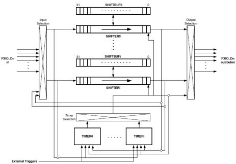
The following figure shows a high-level overview of the module.
Figure 1. Hardware connections diagram
2.2 Internal logic connection
To meet various requirements, the internal logic connections are very flexible and some of them are intricate. Here are some of
the capabilities:
• Any pin/pins can be assigned to a shifter for input or output, as shown in Figure 1.
• Any timer can be assigned to a shifter for shift control, as shown in Figure 1.
• Any pin can be assigned to a timer for timer input or output, as shown in Figure 1.
• Timer triggers can originate from shifter flags, pins, or outside the FlexIO module, as shown in Figure 1.
• The shift can be on the rising or falling edges of the shift clock.
• The pin direction and polarity are configurable.
• The trigger polarity is configurable.
• The timer’s enable, disable, decrement, and reset conditions may originate from the trigger, pin, adjacent timer, and so on.
For detailed information, see the device reference manual.
2.3 Shifters and timers
FlexIO consists of shifters, timers, and pins. The amount of these resources for a given processor can be read from the PARAM
register. For example, the FlexIO module on i.MX RT1010 has 8 shifters, 8 timers, and 32 pins.
The transmit and receive modes are two basic modes of the shifters. When a shifter is in the transmit mode, it loads data from
its buffer register and then shifts the data out to its assigned pin/pins. When a shifter is in the receive mode, it shifts the data from
its assigned pin/pins and then stores the data into its buffer register. The loading, storing, and shifting operations are controlled
by the shifter’s assigned timer.
Using FlexIO to emulate Parallel Camera Interface on i.MX RT, Rev. 0, 01/2020
Application Note 2 / 15NXP Semiconductors
FlexIO overview
The timers can be also configured in different operating modes if needed, including the dual 8-bit counters baud/bit mode, dual
8-bit counters PWM mode, and single 16-bit counter mode.
The dual 8-bit counters' baud/bit mode is usually used to construct a data transmitter. In this mode, the lower 8 bits of the 16-bit
timer divide the module clock source to generate the desired baud rate and the higher 8 bits count the shift bits of a frame. After
it is enabled, the timer loads the initial value from its compare register and starts to count down. When the lower 8 bits decrement
to zero, the timer’s shift clock and its output signal are toggled to generate rising or falling edges. The higher 8 bits count down
by one. The shift clock drives the shifter. The timer output signal usually drives a pin for the clock output, such as the SCK of a
SPI master and the WR of the 8080 bus. After that, the lower 8 bits reload the initial value to start another decrement cycle. The
two decrement cycles make up a shift cycle, which drives the shifter to shift one beat. When all 16 bits decrement to zero, all
data bits in the shifts are shifted out. The timer is then disabled before another transfer frame.
The dual 8-bit counter PWM mode is used to generate PWM outputs. The lower 8 bits are used to configure the high period of
the timer shift clock, and the upper 8 bits are used to configure the low period of the shift clock.
The single 16-bit counter mode is usually used to create a synchronous communication slave, such as the SPI slave, I2S slave,
and so on. All 16 bits are used to configure the timer shift clock.
2.4 Serial and parallel transfers
The FlexIO on the i.MX RT devices supports both serial and parallel transfers. The data is always shifted from the MSB to the
LSB in a shifter for both types of transfers. In the serial transmitter mode, the data is shifted out bit by bit from the LSB (bit 0). In
the serial receiver mode, the data is shifted in bit by bit from the MSB (bit 31). The process is shown in Figure 2-a.
In the parallel transmitter mode, the data is shifted out from the n LSBs of a shifter. In the parallel receiver mode, the data is
shifted in from the n MSBs, where n is the parallel bus width. Figure 2-b shows the use case of n=8.
Figure 2. Serial and parallel transfer diagrams
The following describes the parallel transfer mode:
• The data is shifted n bits on each shift clock, where n is the configured bus width.
• 4, 8, 16, or 32-bit bus widths are supported.
• It combines multiple shifters together for concatenation to support large transfer sizes and use the DMA method to access
the shifter buffer registers for high-speed transfers and low-power operations. The following figure shows the shifter
concatenation diagram, where the additional shifters work as FIFOs.
Using FlexIO to emulate Parallel Camera Interface on i.MX RT, Rev. 0, 01/2020
Application Note 3 / 15NXP Semiconductors
Parallel camera interface
Figure 3. Shifter concatenation for 8-bit parallel transfer diagram
• Only specific shifters (SHIFTER0 and SHIFTER4) support parallel the output to pins. However, all shifters (except for
SHIFTER0) support the output to the adjacent low-order shifters.
• Similarly, only specific shifters (SHIFTER3 and SHIFTER7) support the parallel input from pins. However, all shifters
(except for SHIFTER7) support inputting from the adjacent high-order shifters.
• Any FlexIO pin can be a parallel data output/input pin. However, the pin indexes must be successive for a specific usage,
such as pin0 to pin7, pin1 to pin8, and so on for the 8-bit bus.
2.5 General configurations and operations
The FlexIO can emulate various communication protocols. However, to emulate a dedicated peripheral and to handle the transmit
and receive process, the FlexIO must be configured by software.
Generally, to implement the master transmitter, the shifter is configured in the transmit mode and the assigned timer is configured
in the dual 8-bit counter baud/bit mode. The timer decrement clock originates from the module clock. The timer trigger originates
from the shifter flag with reversed polarity. Filling the shifter buffer via polling/interrupt/DMA clears the shifter flag, which enables
the timer to start count down. The decrement of the timer drives the shifter to shift the data out and generates the clock output
signal.
To implement the receiver, the shifter is configured in the receive mode. The timer is configured in the dual 8-bit counter
baud/bit mode for the synchronous master receiver, such as the 8080-bus reading implementation. This timer mode is also used
for asynchronous receivers, such as the UART receiver. The receive process is similar to that of the master transmitter, but the
data is shifted into the shifter rather than shifted out. For the synchronous receiver, the assigned timer is configured in the single
16-bit counter mode, such as the SPI slave receiver and the parallel camera interface. The decrement clock originates from the
pin input, such as the SPI SCK and the camera PCLK signal. The timer trigger originates from another pin, such as the SPI CS
and the camera HREF signal. The master device enables the timer and controls the decrement via pins. Similarly, the decrement
of the timer drives the shifter to shift in the data.
For the ease of use, NXP provides API drivers and driver examples in the MCUXpresso SDK. You can also find detailed
descriptions and similar APIs of these implementations in various application notes.
3 Parallel camera interface
A parallel camera sensor normally has 8/10/16/24 data lines to output the pixel data and an 8-bit interface camera is most
commonly used. For such camera, if a pixel is in an 8-bit size, one transfer cycle is required. If a pixel is in more than 8 bits,
additional transfer cycles are required. For example, an RGB565 (16-bit) format pixel takes two transfer cycles, and an RGB888
(24-bit) format pixel takes three transfer cycles.
Besides the data lines, there are also timing control outputs VSYNC/VREF, HREF/HSYNC, and PCLK. The following figure shows
the timing diagram of the camera sensor OV7670 used in this application example.
Using FlexIO to emulate Parallel Camera Interface on i.MX RT, Rev. 0, 01/2020
Application Note 4 / 15NXP Semiconductors
Parallel camera interface
Figure 4. Parallel camera interface timing diagram
The figure above shows a frame which contains 510 rows, including 480 valid data lines during VSYNC high. A data line contains
656 points, including 640 valid pixels during HREF high. Therefore, the resolution is VGA (640x480).
In the figure above, two PCLK cycles are used to output 16-bit RGB565/YUV422 format pixel data with the higher byte first and
the lower byte after it.
The data is changed on the PCLK falling edge and latched on the PCLK rising edge.
The frame resolution is adjustable. Different resolutions have similar signal-timing sequences. The following figure illustrates the
timing sequence’s difference between the VGA, QVGA (320x240), and QQVGA (160x120) resolutions.
Using FlexIO to emulate Parallel Camera Interface on i.MX RT, Rev. 0, 01/2020
Application Note 5 / 15NXP Semiconductors
Using FlexIO to emulate parallel camera interface
Figure 5. VGA, QVGA, and QQVGA timing
The figure above shows that the lower the frame resolution is, the longer the HREF blanking area is. The sizes of active areas
from different resolutions are the same. Other signals’ timings are similar for different resolutions.
4 Using FlexIO to emulate parallel camera interface
This section describes how to use the FlexIO to emulate a parallel camera interface with i.MX RT1010.
4.1 Application hardware
The application runs on the SOC validation board, because the available RT1010 EVK board does not have a FlexIO interface
header to connect the camera module. With this document, you can easily run the code on a customized hardware platform. The
following figure shows the hardware connections.
Figure 6. Hardware connections diagram
The following table describes the pin mux configurations for the camera signals.
Table 1. Pin configurations for camera module
RT1010 pin Pin mux function Camera signals
GPIO_09 FLEXIO1_FLEXIO01 OV7670_D0
GPIO_10 FLEXIO1_FLEXIO02 OV7670_D1
GPIO_11 FLEXIO1_FLEXIO03 OV7670_D2
Table continues on the next page...
Using FlexIO to emulate Parallel Camera Interface on i.MX RT, Rev. 0, 01/2020
Application Note 6 / 15NXP Semiconductors
Using FlexIO to emulate parallel camera interface
Table 1. Pin configurations for camera module (continued)
RT1010 pin Pin mux function Camera signals
GPIO_12 FLEXIO1_FLEXIO04 OV7670_D3
GPIO_13 FLEXIO1_FLEXIO05 OV7670_D4
GPIO_SD_00 FLEXIO1_FLEXIO06 OV7670_D5
GPIO_SD_01 FLEXIO1_FLEXIO07 OV7670_D6
GPIO_SD_02 FLEXIO1_FLEXIO08 OV7670_D7
GPIO_SD_03 FLEXIO1_FLEXIO09 OV7670_XCLK
GPIO_SD_04 FLEXIO1_FLEXIO10 OV7670_PCLK
GPIO_SD_05 FLEXIO1_FLEXIO11 OV7670_HREF
GPIO_06 IOMUXC_GPIO_06 (GPIO1_06) OV7670_VSYNC
GPIO_AD_07 LPI2C2_SDA OV7670_SIOD
GPIO_AD_08 LPI2C2_SCL OV7670_SIOC
Note the following about the camera pin mux:
• Cameras D0~D7 must be connected to 8 successive FlexIO pins, such as the FLEXIO1 pins FLEXIO01~FLEXIO08 in this
example.
• XCLK, PCLK, and HREF connect to any of the three FlexIO pins.
• VSYNC connects to a GPIO pin.
• SIOD and SIOC connect to the I2C pins.
The following table describes the pin mux configurations for the LCD signals.
Table 2. Pin configurations for LCD panel
RT1010 pin Pin mux function LCD signals
GPIO_AD_03 LPSPI1_SDI ILI9341_SDO
GPIO_AD_04 LPSPI1_SDO ILI9341_SDI
GPIO_AD_05 LPSPI1_PCS0 ILI9341_CS
GPIO_AD_06 LPSPI1_SCK ILI9341_SCK
GPIO_08 IOMUXC_GPIO_08 (GPIO1_08) ILI9341_DC
GPIO_07 IOMUXC_GPIO_07 (GPIO1_07) ILI9341_RESET
GPIO_SD_13 GPIO2_IO13 ILI9341_LED
Note the following about the LCD pin mux:
• LCD SDO, SDI, CS, and SDK connect to the RT1010 LPSPI pins.
• DC, RESET, and LED connect to the GPIO pins.
4.2 Application software structure
The MCUXpresso SDK is used to build the application software. The MCUXpresso SDK provides peripheral drivers, SOC header
and startup files, various middleware, and example code for various processors from NXP, such as i.MX RT, Kinetis, LPC, and
so on.
Using FlexIO to emulate Parallel Camera Interface on i.MX RT, Rev. 0, 01/2020
Application Note 7 / 15NXP Semiconductors
Using FlexIO to emulate parallel camera interface
The following figure shows the application data flow.
Figure 7. Data flow diagram
The figure above shows that the DMA is used to copy data from the FlexIO to the SRAM and from the SRAM to the LPSPI.
Therefore, the CPU load is very low in such simple applications.
Because the SRAM space is limited (128 KB), the QQVGA (160x120) frame resolution is used.
4.3 Operation principles of FlexIO camera interface
You can configure the FlexIO to emulate a parallel camera interface in different ways, such as with different data bus width,
number of concatenated shifters, and specific shifters, pins, and timers used.
The multi-beat transfer is used to support large transfer sizes. Here, a beat means a shift operation. One transfer sequence
requires the timer to generate multiple shift clocks. The number of beats per one transfer sequence is related to the number of
concatenated shifters and the bus width. One shifter has 32 bits. One shifter supports one 4-beat transfer for an 8-bit bus. Two
shifters support 8 beats and so on. In this application, all 8 shifters are used. Thus, 32 beats are supported for an 8-bit bus.
The following figure shows the FlexIO resources' organization for a parallel camera interface.
Using FlexIO to emulate Parallel Camera Interface on i.MX RT, Rev. 0, 01/2020
Application Note 8 / 15NXP Semiconductors
Using FlexIO to emulate parallel camera interface
Figure 8. FlexIO configuration for parallel camera interface
In the organization, all 8 shifters are concatenated together. TIMER0 is used to control the shifters’ shifting. TIMER1 is used to
generate XCLK (24-MHz in this application). D0-D7, HREF, and XCLK are based on the FlexIO pins. An additional GPIO pin is
used to receive the VSYNC signal. The SHIFTER0 status flag is used to trigger the DMA request.
The process of the transfer is as follows:
1. Configure the FlexIO, DMA, GPIO, and so on. Detailed configurations are shown in the following sections.
2. In a VSYNC rising-edge ISR, retarget the DMA destination address to a new frame buffer.
3. A new line starts to transfer. TIMER0 is enabled by an HREF rising edge.
4. TIMER0 starts to count down along with the PCLK input. At the same time, TIMER0 generates the shift clock controlling
the shifters to shift the data in. The shift clock is generated per one PLCK clock. 8-bit data are shifted per one shift
clock.
5. TIMER0 counts down to zero and a compare event occurs after 32 shift clocks.
6. A storing event is signaled by the compare event. Data are stored from SHIFTER0-SHIFTER7 to shifter buffers
SHIFTBUF0-SHIFTBUF7.
Using FlexIO to emulate Parallel Camera Interface on i.MX RT, Rev. 0, 01/2020
Application Note 9 / 15NXP Semiconductors
Using FlexIO to emulate parallel camera interface
7. The storing event fills up the shifter buffers, which sets the shifters’ status flags and triggers a DMA request.
8. The eDMA copies the data from shifter buffers SHIFTBUF0-SHIFTBUF7 to the SRAM. 32 bytes are copied per one
request.
9. After the compare event, TIMER0 loads the initial value from TIMCMP0 again. Then, steps 4-9 repeat.
10. After the line is transferred, HREF goes to low. TIMER0 is disabled until a new line starts to transfer. Then, steps 3-10
repeat.
11. After the frame is transferred, VSYNC goes to low. Then, steps 2-11 repeat.
This is the process of capturing one frame. The CPU is only required to retarget the DMA destination address in the VSYNC ISR.
All other operations for capturing the frame are done by FlexIO and eDMA. The display DMA source address configuration is
also set in the VSYNC ISR.
4.4 FlexIO configuration for parallel camera interface
The FlexIO configuration for the camera interface mainly consists of the shifter and timer configurations. The following code,
which is clipped from the API driver fsl_flexio_camera.c \ FLEXIO_CAMERA_Init(), implements the shifter configuration.
/* FLEXIO_CAMERA shifter config */
shifterConfig.timerSelect = base->timerIdx;
shifterConfig.timerPolarity = kFLEXIO_ShifterTimerPolarityOnPositive;
shifterConfig.pinConfig = kFLEXIO_PinConfigOutputDisabled;
shifterConfig.pinSelect = base->datPinStartIdx;
shifterConfig.pinPolarity = kFLEXIO_PinActiveHigh;
shifterConfig.shifterMode = kFLEXIO_ShifterModeReceive;
shifterConfig.parallelWidth = FLEXIO_CAMERA_PARALLEL_DATA_WIDTH - 1U;
shifterConfig.inputSource = kFLEXIO_ShifterInputFromNextShifterOutput;
shifterConfig.shifterStop = kFLEXIO_ShifterStopBitDisable;
shifterConfig.shifterStart = kFLEXIO_ShifterStartBitDisabledLoadDataOnEnable;
/* Configure the shifters as FIFO buffer. */
for (i = base->shifterStartIdx; i < (base->shifterStartIdx + base->shifterCount - 1U); i++)
{
FLEXIO_SetShifterConfig(base->flexioBase, i, &shifterConfig);
}
shifterConfig.inputSource = kFLEXIO_ShifterInputFromPin;
FLEXIO_SetShifterConfig(base->flexioBase, i, &shifterConfig);
The code above shows the shifter configurations:
• Timer selection for shifting clock generation: TIMER0 is selected for this application.
• Shifting polarity: Shift is on the positive edge of the Shift clock.
• Shifter Pin I/O configuration: The output is disabled, which means for input only.
• The first data pin selection: Pin 01 is selected in this application. The data pins are 01~08 when the parallel width is 8.
• Shifter pin polarity: The pin is active high, which means that the logic is not reversed from the pin to the shifter.
• Shifter mode: Receive mode.
• Parallel width: 8-bit in this application.
• Input source for the shifter: In this application, the input source of SHIFTER0~SHIFTER6 is the output of
SHIFTER1~SHIFTER7 (respectively) and the input source of SHIFTER7 is from the data pins. This is the shifter
concatenation feature.
• Shifter Stop bit: disabled.
• Shifter Start bit: disabled.
Using FlexIO to emulate Parallel Camera Interface on i.MX RT, Rev. 0, 01/2020
Application Note 10 / 15NXP Semiconductors
Using FlexIO to emulate parallel camera interface
The following code, which is clipped from the API driver fsl_flexio_camera.c \ FLEXIO_CAMERA_Init(), implements the shifting
timer configuration.
timerConfig.triggerSelect = FLEXIO_TIMER_TRIGGER_SEL_PININPUT(base->hrefPinIdx);
timerConfig.triggerPolarity = kFLEXIO_TimerTriggerPolarityActiveHigh;
timerConfig.triggerSource = kFLEXIO_TimerTriggerSourceInternal;
timerConfig.pinConfig = kFLEXIO_PinConfigOutputDisabled;
timerConfig.pinSelect = base->pclkPinIdx;
timerConfig.pinPolarity = kFLEXIO_PinActiveHigh;
timerConfig.timerMode = kFLEXIO_TimerModeSingle16Bit;
timerConfig.timerOutput = kFLEXIO_TimerOutputZeroNotAffectedByReset;
timerConfig.timerDecrement = kFLEXIO_TimerDecSrcOnPinInputShiftPinInput;
timerConfig.timerReset = kFLEXIO_TimerResetOnTimerTriggerRisingEdge;
timerConfig.timerDisable = kFLEXIO_TimerDisableOnTriggerFallingEdge;
timerConfig.timerEnable = kFLEXIO_TimerEnableOnTriggerRisingEdge;
timerConfig.timerStop = kFLEXIO_TimerStopBitDisabled;
timerConfig.timerStart = kFLEXIO_TimerStartBitDisabled;
timerConfig.timerCompare = 8U * base->shifterCount - 1U;
FLEXIO_SetTimerConfig(base->flexioBase, base->timerIdx, &timerConfig);
The code above shows the timer configurations:
• Timer trigger selection: HREF signal pin.
• Trigger polarity: Trigger is active high.
• Trigger source: Internal trigger, which means trigger from the FlexIO module itself.
• Timer pin I/O configuration: Output is disabled, which means for input only.
• Timer pin selection: PCLK signal pin.
• Timer pin polarity: The pin is active high, which means that the logic is not reversed from the pin to the timer.
• Timer mode: 16-bit counter mode.
• Timer output initial state: The timer outputs logic zero when enabled and not affected by the timer reset.
• Timer decrement condition: Counting down on the pin input, the shift clock equals to the pin input.
• Timer reset condition: On the trigger rising edge.
• Timer disablement condition: On the trigger falling edge.
• Timer enablement condition: On the trigger rising edge.
• Timer Stop bit: Disabled.
• Timer Start bit: Disabled.
• Timer compare (initial value): 63. The number of shifting is (63+1)/2=32, which equals the number of bytes in each DMA
transfer.
4.5 FlexIO timer configuration for camera XCLK
Usually, a camera sensor needs a clock source to work. The clock input is usually referred to as PCLK or MCLK. It can be derived
from an oscillator or a clock output from the processor.
The OV7670 camera sensor used in this application requires the clock with the range of 10~48 MHz and the typical value of 24
MHz. In the application, another FlexIO clock TIMER1 is used to generate a 24-MHz clock for this requirement. The following
code, which is clipped from flexio_ov7670.c \ FLEXIO_CameraXclkConfig(), implements the function to configure TIMER1.
timerConfig.triggerSelect = 0u;
timerConfig.triggerPolarity = kFLEXIO_TimerTriggerPolarityActiveHigh;
timerConfig.triggerSource = kFLEXIO_TimerTriggerSourceInternal;
Using FlexIO to emulate Parallel Camera Interface on i.MX RT, Rev. 0, 01/2020
Application Note 11 / 15NXP Semiconductors
Using FlexIO to emulate parallel camera interface
timerConfig.pinConfig = kFLEXIO_PinConfigOutput;
timerConfig.pinSelect = BOARD_CAMERA_FLEXIO_XCLK_PIN_INDEX;
timerConfig.pinPolarity = kFLEXIO_PinActiveHigh;
timerConfig.timerMode = kFLEXIO_TimerModeDual8BitPWM;
timerConfig.timerOutput = kFLEXIO_TimerOutputZeroNotAffectedByReset;
timerConfig.timerDecrement = kFLEXIO_TimerDecSrcOnFlexIOClockShiftTimerOutput;
timerConfig.timerReset = kFLEXIO_TimerResetNever;
timerConfig.timerDisable = kFLEXIO_TimerDisableNever;
timerConfig.timerEnable = kFLEXIO_TimerEnabledAlways;
timerConfig.timerStop = kFLEXIO_TimerStopBitDisabled;
timerConfig.timerStart = kFLEXIO_TimerStartBitDisabled;
timerConfig.timerCompare = 0x0201; /* 120MHz clock source generates 24MHz clock.*/
FLEXIO_SetTimerConfig(BOARD_CAMERA_FLEXIO_INST, 1u, &timerConfig);
The code above shows the timer configurations:
• Timer trigger selection: No trigger is needed for PWM generation. This assignment can have any value.
• Trigger polarity: Trigger is active high.
• Trigger source: Internal trigger.
• Timer pin I/O configuration: Output.
• Timer pin selection: XCLK signal pin.
• Timer pin polarity: The pin is active high, which means that the logic is not reversed from the timer to the pin.
• Timer mode: Dual 8-bit counters PWM mode.
• Timer output initial state: The timer outputs logic zero when enabled and not affected by the timer reset.
• Timer decrement condition: Counting down on the FlexIO module clock (120 MHz in this application), the shift clock
equals the timer output.
• Timer reset condition: Never reset.
• Timer disablement condition: Never disabled.
• Timer enablement condition: Always enabled.
• Timer Stop bit: Disabled.
• Timer Start bit: Disabled.
• Timer compare (initial value): 0x0201. The generated clock frequency from the 120-MHz FlexIO clock is 120/((2+1) + (1
+1)) = 24 MHz. The PWM duty of this configuration is not 50 %. If required, you can configure the value to 0x0202, which
generates 20-MHz 50 % duty waveform.
4.6 DMA TCD configurations
When the frame data is shifted in and the shifters are full, the data must be read out to the memory in time to avoid overflow. The
eDMA is used for the data transfer to lower the CPU load. The following code, which is clipped from flexio_ov7670.c \ configDMA
(), implements the DMA TCD (Transfer Control Descriptor) configuration.
/* Configure DMA TCD */
DMA0->TCD[FLEXIO_CAMERA_DMA_CHN].SADDR = FLEXIO_CAMERA_GetRxBufferAddress(&s_FlexioCameraDevice);
DMA0->TCD[FLEXIO_CAMERA_DMA_CHN].SOFF = 0u;
DMA0->TCD[FLEXIO_CAMERA_DMA_CHN].ATTR = DMA_ATTR_SMOD(0u) | DMA_ATTR_SSIZE(5u) |
DMA_ATTR_DMOD(0u) | DMA_ATTR_DSIZE(5u);
DMA0->TCD[FLEXIO_CAMERA_DMA_CHN].NBYTES_MLNO = 32u;
DMA0->TCD[FLEXIO_CAMERA_DMA_CHN].SLAST = 0u;
DMA0->TCD[FLEXIO_CAMERA_DMA_CHN].DADDR = (uint32_t)(*pFlexioCameraFrameBuffer);
DMA0->TCD[FLEXIO_CAMERA_DMA_CHN].DOFF = 32u;
DMA0->TCD[FLEXIO_CAMERA_DMA_CHN].CITER_ELINKNO = (OV7670_FRAME_BYTES / 32u);
Using FlexIO to emulate Parallel Camera Interface on i.MX RT, Rev. 0, 01/2020
Application Note 12 / 15NXP Semiconductors
Using FlexIO to emulate parallel camera interface
DMA0->TCD[FLEXIO_CAMERA_DMA_CHN].DLAST_SGA = 0;
DMA0->TCD[FLEXIO_CAMERA_DMA_CHN].CSR = 0u;
DMA0->TCD[FLEXIO_CAMERA_DMA_CHN].CSR |= DMA_CSR_DREQ_MASK;
DMA0->TCD[FLEXIO_CAMERA_DMA_CHN].BITER_ELINKNO = (OV7670_FRAME_BYTES / 32u);
The code above shows the DMA TCD configurations:
• Source address: FlexIO SHIFTBUF0 address.
• Source address offset: 0, which means no offset.
• Source address modulo: 0, which means that the source address modulo is disabled.
• Source data transfer size for each time access: 5, which means 32 bytes burst.
• Destination address modulo: 0, which means that the destination address modulo is disabled.
• Destination data transfer size for each time access: 5, which means 32 bytes burst.
• Minor loop byte count: 32 bytes.
• Source minor loop offset mapping: Disabled.
• Destination minor loop offset mapping: Disabled.
• Last source address adjustment: 0, which means no adjustment.
• Destination address: RAM buffer address.
• Destination address offset: 0, which means no offset.
• Major loop counter: (OV7670_FRAME_BYTES / 32u) = (160 x 120 x 2) / 32 = 1200.
• Last destination address adjustment: 0, which means no adjustment. The new destination address is configured in the
VSYNC ISR.
• Disable the DMA request after each major loop. The request is enabled in the VSYNC ISR each time.
4.7 FlexRAM configuration
The 128-KB internal RAM of RT1010 can be configured to be ITCM, DTCM, or OCRAM using the FlexRAM feature. By default,
the 128-KB RAM is divided into 32-KB ITCM, 32-KB DTCM, and 64-KB OCRAM.
On the other hand, one whole frame in this application takes up 160 x 120 x 2 = 38.4 KB. One frame buffer can be placed into
the OCRAM. However, if two frame buffers are used with the ping-pong buffering way, the default RAM allocation would not be
applicable. The following code, which is clipped from startup_MIMXRT1011.s, illustrates how to reallocate the RAM for the
application. The reason why this configuration is implemented in the startup assembly file is to make sure that no stacking
operation is executed before the reallocation. The stack address can be updated during the reallocation.
LDR R0, =0x400AC044 ;IOMUXC_GPR_GPR17 register
LDR R1, =0x000000D5
STR R1, [R0]
LDR R0, =0x400AC040 ;IOMUXC_GPR_GPR16 register
LDR R1, =0x00000007
STR R1, [R0]
The 128-KB RAM is divided into 32-KB ITCM and 96-KB OCRAM. In addition, the linker script file must be updated to match the
new RAM space. The code below shows the updated section of the IAR linker script file.
define symbol m_data2_start = 0x20200000;
define symbol m_data2_end = 0x20217FFF;
define region DATA2_region = mem:[from m_data2_start to m_data2_end];
define region CSTACK_region = mem:[from m_data2_end-__size_cstack__+1 to m_data2_end];
place in DATA2_region { block RW };
place in DATA2_region { block ZI };
Using FlexIO to emulate Parallel Camera Interface on i.MX RT, Rev. 0, 01/2020
Application Note 13 / 15NXP Semiconductors
Conclusion
place in DATA2_region { last block HEAP };
place in DATA2_region { block NCACHE_VAR };
place in CSTACK_region { block CSTACK };
A region named DATA2_region is defined to represent the 96-KB OCRAM. The blocks RW, ZI, HEAP, NCACHE_VAR, and
CSTACK are all placed into this region.
The frame buffers are defined in the NCACHE_VAR block with the following code clipped from flexion_ov7670.c.
typedef uint16_t FrameBuffer_t[OV7670_FRAME_HEIGHT][OV7670_FRAME_WIDTH];
#pragma data_alignment = 32
static FrameBuffer_t g_FlexioCameraFrameBuffer[OV7670_FRAME_BUFFER_CNT] @"NonCacheable";
5 Conclusion
This application note describes the use of FlexIO to emulate the parallel camera interface with the i.MX RT1010 processor. The
demo application uses the OV7670 camera module, which is configured to output QQVGA frames. The frame rate is up to 30 fps.
With this example, you can use the low-cost RT1010 processor in your applications with the alternative parallel camera interface.
6 References
• i.MX RT1010 Reference Manual (document IMXRT1010RM)
• Using FlexIO for Parallel Camera Interface (document AN5275)
• Generating PWM Using FlexIO (document AN5209)
• Using FlexIO to Drive 8080 Bus Interface LCD Module (document AN5313)
Using FlexIO to emulate Parallel Camera Interface on i.MX RT, Rev. 0, 01/2020
Application Note 14 / 15How To Reach Us Information in this document is provided solely to enable system and software implementers to
use NXP products. There are no express or implied copyright licenses granted hereunder to
Home Page:
design or fabricate any integrated circuits based on the information in this document. NXP
nxp.com reserves the right to make changes without further notice to any products herein.
Web Support: NXP makes no warranty, representation, or guarantee regarding the suitability of its products for
nxp.com/support any particular purpose, nor does NXP assume any liability arising out of the application or use
of any product or circuit, and specifically disclaims any and all liability, including without limitation
consequential or incidental damages. “Typical” parameters that may be provided in NXP data
sheets and/or specifications can and do vary in different applications, and actual performance
may vary over time. All operating parameters, including “typicals,” must be validated for each
customer application by customer's technical experts. NXP does not convey any license under
its patent rights nor the rights of others. NXP sells products pursuant to standard terms and
conditions of sale, which can be found at the following address: nxp.com/
SalesTermsandConditions.
While NXP has implemented advanced security features, all products may be subject to
unidentified vulnerabilities. Customers are responsible for the design and operation of their
applications and products to reduce the effect of these vulnerabilities on customer’s applications
and products, and NXP accepts no liability for any vulnerability that is discovered. Customers
should implement appropriate design and operating safeguards to minimize the risks associated
with their applications and products.
NXP, the NXP logo, NXP SECURE CONNECTIONS FOR A SMARTER WORLD, COOLFLUX,
EMBRACE, GREENCHIP, HITAG, I2C BUS, ICODE, JCOP, LIFE VIBES, MIFARE, MIFARE
CLASSIC, MIFARE DESFire, MIFARE PLUS, MIFARE FLEX, MANTIS, MIFARE ULTRALIGHT,
MIFARE4MOBILE, MIGLO, NTAG, ROADLINK, SMARTLX, SMARTMX, STARPLUG, TOPFET,
TRENCHMOS, UCODE, Freescale, the Freescale logo, AltiVec, C‑5, CodeTEST, CodeWarrior,
ColdFire, ColdFire+, C‑Ware, the Energy Efficient Solutions logo, Kinetis, Layerscape, MagniV,
mobileGT, PEG, PowerQUICC, Processor Expert, QorIQ, QorIQ Qonverge, Ready Play,
SafeAssure, the SafeAssure logo, StarCore, Symphony, VortiQa, Vybrid, Airfast, BeeKit,
BeeStack, CoreNet, Flexis, MXC, Platform in a Package, QUICC Engine, SMARTMOS, Tower,
TurboLink, UMEMS, EdgeScale, EdgeLock, eIQ, and Immersive3D are trademarks of NXP B.V.
All other product or service names are the property of their respective owners. AMBA, Arm,
Arm7, Arm7TDMI, Arm9, Arm11, Artisan, big.LITTLE, Cordio, CoreLink, CoreSight, Cortex,
DesignStart, DynamIQ, Jazelle, Keil, Mali, Mbed, Mbed Enabled, NEON, POP, RealView,
SecurCore, Socrates, Thumb, TrustZone, ULINK, ULINK2, ULINK-ME, ULINK-PLUS, ULINKpro,
µVision, Versatile are trademarks or registered trademarks of Arm Limited (or its subsidiaries) in
the US and/or elsewhere. The related technology may be protected by any or all of patents,
copyrights, designs and trade secrets. All rights reserved. Oracle and Java are registered
trademarks of Oracle and/or its affiliates. The Power Architecture and Power.org word marks
and the Power and Power.org logos and related marks are trademarks and service marks
licensed by Power.org.
© NXP B.V. 2020. All rights reserved.
For more information, please visit: http://www.nxp.com
For sales office addresses, please send an email to: salesaddresses@nxp.com
Date of release: 01/2020
Document identifier: AN12686You can also read