AN5650 VIPower transient thermal analysis using SPICE
←
→
Page content transcription
If your browser does not render page correctly, please read the page content below
AN5650

                                                                      VIPower transient thermal analysis using SPICE

Introduction
Calculating transient thermal response in a high side driver can get very complicated. To be accurate, transient thermal analysis
should include conduction losses, switching losses, supply current losses as well as clamping energy at turn off.
ST provides a solution using a thermal analysis tool called TwisterSIM that can be downloaded from ST web page (TwisterSIM).
TwisterSIM is very useful to determine the dynamic thermal response to transients from inrush to stall including clamping
energy capability. TwisterSIM also provides first level selection guide based on some of application requirements. Please refer
to UM1874 for details on how to use TwisterSIM.
TwisterSIM works well for short duration analyses. Durations of more than a few seconds, however, can take enormous
amounts of time to process. In this case ST provides a Foster model in every VIPower high side driver datasheet that is similar
to what is used in TwisterSIM. With this model, longer duration dynamic thermal analyses can be performed in SPICE.
The effort comes in modelling the power dissipation. Conduction losses are more than a simple square of the current multiplied
by the on-resistance (RDS(on)) of the switch. The RDS(on) changes with temperature and doubles between 25 °C and 150 °C.
This change in on-resistance (RDS(on)) dramatically affects the power dissipated in the switch. As a result, a few elements need
to be added to the basic Foster model provided in every VIPower datasheet.
This application note describes the process of adding the power dissipation elements to make an accurate long-term thermal
analysis. This is not intended to analyze shorted loads or to emulate the functionality of the high side driver (that are thermal
intervention, current limit, or inductive clamping), but to provide a thermal response to various complex loads not easily
simulated in TwisterSIM. For the M07 high side driver protection strategy please refer to AN5368.

AN5650 - Rev 1 - April 2021                                                                                                www.st.com
For further information contact your local STMicroelectronics sales office.
AN5650
                                                                                                   The Foster thermal impedance model

1                The Foster thermal impedance model

                 In every VIPower M07 high side driver datasheet there is a six order Foster model for thermal impedance. The
                 Foster model includes provisions for each the outputs. Each model is created by curve fitting from actual thermal
                 testing results. That means the elements do not necessarily fit the natural boundaries of an IC (die, package,
                 circuit board). There is some correlation, however it is not intentional. The first few elements tend to be die related
                 just due to their time constants. The last few elements are more related to the circuit board thermal capability.

                                       Figure 1. Six order Foster model equivalent circuit for a 2-channel HSD

                 When using the above model in SPICE, the current represents the power dissipation and voltage represents the
                 temperature. The channel power dissipation components can be simulated using or manipulating various current
                 sources available on SPICE. The equivalent resistors and capacitors are adjusted based on the circuit board heat
                 sinking area. The values for these components also vary depending on the device package and die size. The
                 parameters used to fill in the Foster model are found in all M07 VIPower high side driver datasheets (see Table 1).

                                            Table 1. Example of a thermal parameter table (VND7050AJ)

                    Area/island (cm2)            Footprint                  2                      8                       4L

                     R1 = R7 (°C/W )                1.8
                     R2 = R8 (°C/W )                3.2
                       R3 (°C/W )                   8                       8                      8                       6
                       R4 (°C/W )                   14                      6                      6                       4
                       R5 (°C/W )                   30                     20                      10                      3
                       R6 (°C/W )                   26                     20                      18                      7
                    C1 = C7 (Ws/°C )             0.00035
                    C2 = C8 (Ws/°C )              0.005
                       C3 (Ws/°C )                 0.05
                       C4 (Ws/°C )                  0.2                    0.3                     0.3                    0.4
                       C5 (Ws/°C )                  0.4                     1                      1                       4
                       C6 (Ws/°C )                  3                       5                      7                       18

                 This basic model provides for the thermal impedances based on four different circuit board layouts. It is possible
                 choose from one of these four layouts or estimate something in between based on specific layout.

AN5650 - Rev 1                                                                                                                  page 2/25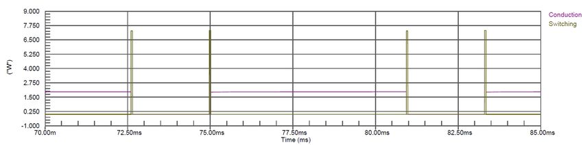
AN5650
                                                                                                          Modelling power elements

2                Modelling power elements

                 SPICE simulators can easily incorporate the Foster models found in our datasheets. A few elements need to
                 be added for this model to provide accurate junction temperatures. This can be broken down into their separate
                 contributions.
                 •     Conduction losses
                 •     Switching losses
                 •     Supply current losses
                 The power losses can be modelled in many ways. The below schematic illustrates two different ways of modelling
                 the power losses due to load current. The current and power dissipation sources discussed here are just two
                 ways available. SPICE is capable to simulate several combinations of power losses.

                                            Figure 2. Foster thermal model including power sources

2.1              Initial conditions
                 Initial conditions are essentially the ambient temperature at the start of an evaluation. These are defined by
                 the ICx control statements and the TAmb voltage source in the schematic in Figure 2. The initial conditions are
                 mandatory in ensuring the proper thermal analysis. Typically, the initial conditions and the ambient temperature
                 (represented as a voltage) are the same. In the schematic example of Figure 2, the ambient temperature and
                 initial conditions are 85 V.

2.2              Conduction losses
                 The on-resistance (RDS(on)) of the switch is dependent on the junction temperature. To compensate for this
                 dependency, a two stage simulation is implemented. This replaces the PdChx piecewise linear estimation of
                 power found in the datasheet model with a two-stage system where the current is first defined and then the power
                 dissipation can be dynamically calculated using that defined current with the junction temperature (TJx).
                 In the schematic shown in Figure 2, ILOAD_Chx is used to define the actual load current. Then the second stage,
                 PdCHx, calculates the resulting power using an equation that includes the temperature effects on RDS(on).

AN5650 - Rev 1                                                                                                              page 3/25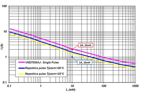
AN5650
                                                                                                                Conduction losses

2.2.1            Load current definition
                 •    Periodic (PWM) outputs.
                      Load current can be defined in any way that is convenient for the waveform. In the above example,
                      ILOAD_Ch1 is a pulse width modulated signal set with a 71% duty cycle at 120 Hz. Because this is a
                      periodic signal with some frequency, switching losses are also considered as another power contributor.
                      This output power then has two contributors, conduction and switching. These are mutually exclusive
                      contributors. While the driver is switching, the conduction losses are not considered and vice versa.
                 •    Non periodic outputs.
                      Non-periodic or odd duration waveforms can be described using piecewise linear (IPWL) function in SPICE.
                      ILOAD_Ch2 for example, is a simple piecewise linear step function. Because it is not a PWMmed output
                      switching losses do not need to be considered. A motor inrush, run, and stall currents can be emulated in
                      this manner.

2.2.2            Calculating the conduction losses
                 The second stage takes the predefined current and converts it to power using the junction temperature to adjust
                 the RDS(on). A reasonable approximation of on-resistance for worst case analysis doubles the RDS(on) between
                 25 °C and 150 °C. The Equation 1 provides a simple linear interpolation reflecting the thermal characteristics
                 of on-resistance over temperature. This is not exact. However, it is accurate enough for worst case calculation
                 purposes.

                 Equation 1 – Junction temperature compensated RDS(on)

                                                                                   T J − 25 ºC
                                                   RDS on = RDS on @ 25 ºC 1 +                                                  (1)
                                                                                     125 ºC

                 This can be simplified to be more easily implemented in SPICE.

                 Equation 2 – Junction temperature compensated RDS(on) simplified

                                                 RDS on T J = RDS on @ 25 ºC 0.8 + 0.008T J                                     (2)

                 The simple I2R power equation for conduction losses then looks like:

                 Equation 3 – Conduction losses with respect to temperature

                                               PCOND = IOUT2 × RDS on @ 25 ºC 0.8 + 0.008T J                                    (3)

                 What this looks like in SPICE for OUT0 using a 50 mΩ switch (VND7050AJ):

                 Equation 4 – Current to power equation estimation for SPICE model
                                            BPdCℎ0 0 TJ0 I = V SNS0 ∧ 2 * 0.05 * 0.8 + 0.008 * V TJ0                            (4)

                 Where:
                 •   BPdCh0 is calculated power dissipation due to conduction losses in Ch0
                 •   V(SNS0) is the voltage seen at the SNS0 node (ILOAD_Ch0 * 1 Ω)
                 •   0.05 is the output on-resistance at 25 °C for Ch0 (RDS(on) @ 25 ºC = 50 mΩ).
                 •    V(TJ0) is the measured junction temperature at the Ch0 node (TJ0).

AN5650 - Rev 1                                                                                                            page 4/25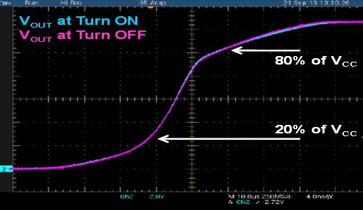
AN5650
                                                                                                                         Switching losses

3                Switching losses

                 Switching losses are a result of the driver behaving as a linear output for very short periods of time. The output is
                 neither on nor off. It is being driven linearly from one rail to the other. As a result, switching losses are calculated
                 using voltage and current (as opposed to I2R).

                 Equation 5 – Basic power equation during switching

                                                           PSwitcℎ t = VOUT t × IOUT t                                                 (5)

                 The Figure 4 illustrates the switching losses in a simple trapezoidal output. With this simple illustration, we can
                 see that EMI comes from the “corners” of the waveform and the power dissipation is mostly in the middle of the
                 transition. To reduce switching losses the slew rate needs to be fast. However, to reduce EMI the opposite is true.

                                                Figure 3. Resistive load switching losses waveform

                 To reduce EMI while reducing switching losses, ST’s VIPower high side drivers have rather sophisticated turn
                 on/off slopes. These are purposely done to reduce EMI while keeping switching losses to a minimum. This makes
                 trapezoidal estimation of switching losses rather complicated.

                                      Figure 4. Typical VIPower M07 high side driver switching waveforms

                 With that, switching losses for VIPower high side drivers are expressed in terms of specification parameters, Won
                 and Woff. These parameters define the energy consumed during a single switch event (rise or fall) at a specific
                 load and supply voltage. The advantage is a much simpler method of calculating an accurate value for switching
                 losses.

AN5650 - Rev 1                                                                                                                   page 5/25
AN5650
                                                                                                    Switching losses as a DC average

                                                  Table 2. Switching losses definition (VND7050AJ)

                 VCC = 13 V, -40 ºC < TJ < 150 ºC, unless otherwise specified

                     Symbol                           Parameter                       Test conditions    Min.    Typ.   Max.     Unit

                      Won       Switching energy losses at turn-on (twon)           RL = 6.5 Ω             -     0.25   0.33      mJ

                      Woff      Switching energy losses at turn-off (twoff)         RL = 6.5 Ω             -     0.23   0.31      mJ

                 Switching losses can be calculated in a number of ways using the parameters of Table 2. The simplest is
                 calculating the average DC power loss and adding that to the junction temperature (TJx) node. For a more
                 detailed examination of switching losses two pulse current sources can be used, one for rise time and one for fall
                 time. Again, these pulse current sources would be inserting current into the TJx nodes (reference the TJ0 node in
                 Figure 2). Switching losses affect junction temperature and as a result affect RDS(on). However, RDS(on) does not
                 affect switching losses. Therefore, contributions to switching losses are not inserted as a part of the conduction
                 losses calculation.

3.1              Switching losses as a DC average
                 The simplest way to insert switching losses is incorporating a DC estimation of switching losses. This is more
                 than sufficient for most thermal evaluations. It is by far the simplest to calculate. To calculate the losses due to
                 switching requires multiplying the sum of the two switching parameters (Won and Woff) by the switching frequency.
                 This however is only accurate at the voltage and load specified in the datasheet.

                 Equation 6 – Switching losses using Won and Woff

                                                              PSwitcℎ = Won + Woff freq                                              (6)

                 Switching losses, in however complex the waveform might be, are still essentially voltage multiplied by current.
                 With that we can “adjust” the losses due to switching by swapping out the specified voltage and load for the
                 application voltage and load. The VIPower M07 specifications use a load resistance to specify the Won / Woff
                 losses. The typical load definition is in terms of current. As a result, the following equation can be used to
                 calculate the average switching losses (for a resistive load).

                 Equation 7 – Resistive switching losses using Won and Woff adjusting for application conditions

                                                                I   V     RL
                                                      PSw_avg = new new      Won + Woff freq                                         (7)
                                                                  Vspec 2

                 Where:
                 •   PSw_avg are the adjusted resistive load switching losses
                 •    Vnew is the application supply voltage
                 •    Inew is the application load current
                 •    RL is the load resistance used to specify the Won/Woff parameters
                 •    Vspec is the supply voltage used to specify the Won/Woff parameters (13 V)

                 With this calculation the average power dissipated due to switching losses can be inserted into the TJx node
                 as shown in Figure 5. This does not generate in the simulation results the “bumps” in junction temperature due
                 to switching. It does, however, provide a reasonable job of representing the elevation of the average junction
                 temperature over time.

AN5650 - Rev 1                                                                                                                 page 6/25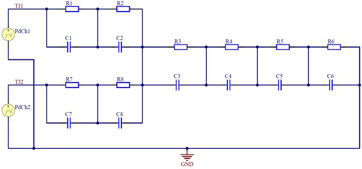
AN5650
                                                                                              Instantaneous switching losses simulation

                                             Figure 5. Inserting average switching power dissipation

                 Inductive loads with a freewheeling diode generate a bit more power when switching. Due to the geometry of
                 the waveforms, inductive load switching losses can use the same switching losses Equation 7 multiplied by 3.
                 However, VIPower M07 high side drivers tend to switch too slowly for the switching frequency needed for most
                 inductive loads. A quick switching losses calculation can easily illustrate this.

3.2              Instantaneous switching losses simulation
                 To calculate the instantaneous switching losses two pulse current sources are used. One defines the rise, or
                 turn-on, losses and one defines the fall, or turn-off, losses. They are different for two reasons. First, they are not
                 the same amplitude. Second, unless the duty cycle is 50%, they occur at different places in the period.

                                                        Figure 6. Simulated switching losses

                 Since switching losses and conduction losses are mutually exclusive care must be taken to ensure that they do
                 not overlap. This means offsetting the pulses to sit just prior to turn-on and just after turn-off.

                                          Figure 7. Switching and conduction losses simulation results

                 Offsets take into account the rise time parameter duration. Each pulsed waveform has a rise time, a duration, and
                 a fall time. These are additive. Setting the waveform rise and fall times to zero eliminates any possible thermal
                 contribution due to overlap. It is important to remember that this is a simulation where power sources are super
                 positioned so that they represent actual power being dissipated. Realistic rise and fall times are not required. Only
                 the final, superposed result is relevant.

AN5650 - Rev 1                                                                                                                   page 7/25
AN5650
Instantaneous switching losses simulation
3.2.1 Calculating the output rise and fall times
Rise and fall times are not provided in the VIPower high side driver datasheets. ST provides the expected slew
rates. From these parameters it can derive the expected rise and fall times with a simple equation.
Table 3. Switching parameters for the VND7050AJ
VCC = 13 V, -40 ºC < TJ < 150 ºC, unless otherwise specified
Symbol Parameter Test conditions Min. Typ. Max. Unit
td(on) Turn-on delay time at TJ = 25 ºC 10 60 120 μs
RL = 6.5 Ω
td(off) Turn-off delay time at TJ = 25 ºC 10 40 10 μs
(dVOUT/dt)on Turn-on voltage slope at TJ = 25 ºC 0.1 0.3 0.7 V/μs
RL = 6.5 Ω
(dVOUT/dt)off Turn-off voltage slope at TJ = 25 ºC 0.1 0.32 0.7 V/μs
The rise and fall time durations can be calculated using the above parameters and the application supply voltage:
Equation 8 – Rise time calculation
Vsupply
trise = (8)
dVOUT
dt on
Equation 9 – Fall time calculation
Vsupply
tfall = (9)
dVOUT
dt off
Where :
• trise is the duration used for the rise time in the simulation (reference from Figure 2: rise_0)
• tfall is the duration used for the fall time in the simulation (reference from Figure 2: fall_0)
• Vsupply is the supply voltage of the application
• (dVOUT/dt)on is the rise time slew rate given in the datasheet
• (dVOUT/dt)off is the fall time slew rate given in the datasheet
The slew rate parameters in the datasheet include the minimum, typical and maximum values. For simplicity the
typical value can be used. The energy is the same and the overall junction temperature is the same as the energy
dissipated is the same. The only difference is a slight peak in junction temperature when using the faster slew
rates. This is because there is the same amount of energy being dissipated over a shorter duration.
3.2.2 Calculating the energy in each transition
As mentioned in Section 3.1 , the Won and Woff parameters are only valid at 13 V at the load resistance
specified. As a result, some adjustment need to be done to accommodate for different supply voltages and
loads. Secondly, it needs to spread the calculated power over the switching duration. It is not ideal in that
the simulation (a square pulse) does not reflect perfectly the actual instantaneous power during the transition
(somewhat sinusoidal). However, it is close enough for this purpose.
By adapting Equation 7 the supply and load differences for each transition can be calculated:
Equation 10 – Adjusting Won for supply and load
I V RL
ESw_on = new new Won (10)
Vspec2
AN5650 - Rev 1 page 8/25AN5650
Instantaneous switching losses simulation
Equation 11 – Adjusting Woff for supply and load
I V RL
ESw_off = new new Woff (11)
Vspec 2
Turning these into equivalent currents for the simulation requires to divide the result by the transition times and
obtain Joules per second (J/s = W) for the duration of the switch.
Equation 12 – Calculating power during switching (rise time)
dVOUT
InewRL
ESw_on dt on W
PSw_on =
trise = on (12)
Vspec2
Equation 13 – Calculating power during switching (fall time)
dVOUT
ESw_off InewRL
dt off
PSw_off =
tfall = Woff (13)
Vspec2
AN5650 - Rev 1 page 9/25AN5650
Clamping inductive energy
4 Clamping inductive energy
Driving inductive loads without a freewheeling diode is possible. Care must be taken to ensure to not exceed
the inductive energy capability of the driver at turn off. Excessive power dissipation due to high clamping energy
can cause inelastic thermo-mechanical stress on the surface of the silicon. That is, the silicon expands rapidly
and unevenly, heating up faster where the power dissipation is the highest. When the device cools, the silicon
does not completely return to the original size. This phenomenon can be defined using the Coffin-Mason thermal
fatigue model. This model defines the highest thermal gradient across the die without causing inelastic expansion
to be approximately 60 °C.
Equation 14 – Coffin-Mason thermal fatigue model
Nf = Af−α × ΔT−β × G TMAX (14)
where:
• Nf is the number of cycles to failure
• f is the cycling frequency
• ΔT is the range of temperature during the cycle
• G(TMAX) is an Arrhenius term evaluated at the max temperature reached during the cycle
• α is 2 (typically)
• β is 1/3 (typically)
As a result, this thermal gradient must be avoided. The best way to do this is to calculate the inductance and
current and plot that on the current vs inductance plots given in the datasheets (see Figure 8).
Figure 8. VND7050AJ maximum turn off energy plot
Looking at the Figure 8, anything below the lines are safe. For instance:
• A 1 A, 10 mH load is safe for both repetitive as well as single pulses. That is, this amount of energy does not
degrade the device. However, repetitive pulses may add enough heat to overheat the part.
• A 2 A, 10 mH load exceeds the repetitive pulse limits. It is marginal for single events and should be verified
in TwisterSIM.
If either of the parameters (current or inductance) are not inside the plot definitions, then you can run the
simulation in TwisterSIM. Calculating the effects of clamping inductive energy is a short-term simulation and can
be easily performed in TwisterSIM. If TwisterSIM determines that the load inductance is more than the device will
be able to reliably handle, then a warning is displayed (see Figure 9).
AN5650 - Rev 1 page 10/25AN5650
Clamping inductive energy
Figure 9. TwisterSIM excessive inductance warning
The TwisterSIM simulation results indicate if the junction temperature transition during the clamping function
exceeds a safe level. If it does, then a freewheeling diode may be needed.
If repetitive clamping an inductive load is not too much inductive energy (see Figure 8), then the contribution
to the thermal load can be estimated using a DC average. Then, the contribution to the thermal load can be
estimated using a DC average. This is because the thermal peak is diffused into the driver long before the driver
is turned back on.
DC average power (W) is done by calculating the energy (J) consumed in the driver and multiplying it by the
frequency (J/s = W).
Calculating the energy during a clamp requires a bit more math than just calculating the energy in the inductor.
This is because the driving circuit is also providing the clamping through the supply and not directly through
ground back into the inductor (see Figure 10).
Figure 10. Current flow during inductive clamp
An s-domain equation can be written to describe the system in Figure 10. That equation can be transformed into
the time domain by a Laplace transform. The resulting time domain equation is then solved for the current shown
in Equation 15 below:
Equation 15 – Clamping current equation
RIt
IClamp t = VClamp − VBatt − VClamp − VBatt − IOUTRI e− LI (15)
Solving this for tClamp at 0 A provides the clamp duration:
Equation 16 – Clamping duration
L IOUTRI
IClamp = I ln 1 − (16)
RI VClamp − VBatt
Integrating the power (VClamp x IClamp(t)) over the clamping duration (tClamp) we obtain:
Equation 17 – Clamping energy
LIVClamp VClamp − VBatt
EClamp = VClamp − VBatt ln + IOUTRI (17)
RI2 VClamp − VBatt + IOUTRI
AN5650 - Rev 1 page 11/25AN5650
Clamping inductive energy
Multiplying this by the frequency obtains the average power dissipated by the clamping function.
Equation 18 – Average power dissipation due to repetitive clamping
LIVClamp VClamp − VBatt
PClamp_avg = VClamp − VBatt ln (18)
RI2 VClamp − VBatt + IOUTRI
+ IOUTRI freq
This can be added as a DC current source into the circuit:
Figure 11. Inserting the average power dissipation due to clamping
AN5650 - Rev 1 page 12/25AN5650
Supply current power dissipation calculations (Psupply)
5 Supply current power dissipation calculations (Psupply)
Losses due to quiescent current are simply the supply voltage multiplied by the supply current. Care must be
taken to choose the correct current from the datasheet. The current to use is IGND(ON). This parameter defines the
current coming out of the ground pin while the outputs are under a load. The supply current changes with load
current. This is because there is current out of the multisense pin that mirrors a portion of current from the high
side switch. The portion of current from the high side switch shows up on the ground pin. As a result, the ground
current changes depending on the output current(s).
Table 4. Supply current parameter, IGND(ON) (VND7050AJ)
Symbol Parameter Test conditions Min. Typ. Max. Unit
VCC = 13 V, VSEn = 5 V,
Control stage current
IGND(ON) consumption in ON state. All VFR = VSEL0, 1 = 0 V, VIN0 = 5 V, VIN1 = 5 V, - - 12 mA
channels active.
IOUT0 = 2 A, IOUT0 = 2 A
This power dissipation is created in the control section of the die. As a result, the Psupply current is injected after
the channel-only elements in the Foster model. That is, the current (power) is inserted before the R3, C3 element
pair (refer to Figure 2).
AN5650 - Rev 1 page 13/25AN5650
Programming the elements (summary)
6 Programming the elements (summary)
This section provides a summary of the different elements used in Figure 2.
6.1 Conduction losses definitions
Current definition has two components. First to describe the load current accurately then to calculate the power as
a result of that current.
6.1.1 Current definition for conduction losses
To accommodate for the rise time the current is delayed by the rise time. This allows the switching losses at
turn-on not to overlap with the conduction losses.
PWM current parameters (for our example ILOAD_Ch0):
• Initial value is 0
• Pulsed value is application current (the example in Figure 2 uses 5 A)
• Time delay is trise (from Equation 8 above)
• Rise time is 0 s
• Fall time is 0 s
• Pulse width is duty/PWM frequency
• Period is 1/PWM frequency
A SPICE PWM load current definition (example) is:
ILOAD_Ch0 0 SNS0 DC 0 PULSE(0 5 45us 0s 0s 5.92ms 8.33ms) AC 1 0
Piecewise linear current definitions are typically used for on/off loads where the current changes naturally during
the course of driving it. A good example would be a motor load current definition. This definition would have
inrush, run, and stall currents while the switch is only turned on at the beginning and off at the end.
A SPICE PWL load current definition (example) is:
ILOAD_Ch1 0 SNS1 DC 0 PWL(0 0 3 0 3.01 5 10 5) AC 1 0
6.1.2 Power calculations for conduction losses
The power calculation is a simple equation illustrated in Section 2.2.2 . The only changes to this equation
are done to accommodate for the different RDS(on) values in the different switches. The below example shows
a different nodal connection for the PWMed output as sense resistors (Rsense and Rsensesw) were added to
enable visibility to the power injected into the junction.
The power dissipation calculation SPICE command using pre-defined load currents (example) is:
BPdCh0 NetPdCh0_1 TJ0 I=V(SNS0)^2*0.050*(0.8+0.008*V(TJ0))
BPdCh1 0 TJ1 I=V(SNS1)^2*0.05*(0.8+0.008*V(TJ1))
AN5650 - Rev 1 page 14/25AN5650
Switching losses definitions
6.2 Switching losses definitions
6.2.1 Rise time definitions
The rise time starts off the simulation. There is no delay associated with it.
trise parameters (for our example rise_0) are:
• Initial value is 0 s
• Pulsed value is PSw_on as calculated in Equation 10
• Time delay is 0 s
• Rise time is 0 s
• Fall time is 0 s
• Pulse width is trise (from Equation 8)
• Period is 1/frequency
The rise time power SPICE command line (example) is:
Irise_0 Netfall_0_1 TJ0 DC 0 PULSE(0 7.3333 0 0s 0s 45us 8.33ms) AC 1 0
6.2.2 Fall time definitions
The fall time is delayed by both the rise time and the duty cycle (on time).
tfall parameters (for proposed example fall_0) are:
• Initial value is 0
• Pulsed value is PSw_off as calculated in Equation 11
• Time delay is duty/frequency + trise
• Rise time is 0 s
• Fall time is 0 s
• Pulse width is tfall (from Equation 9)
• Period is 1/frequency
The fall time power SPICE command line (example) is:
Ifall_0 Netfall_0_1 TJ0 DC 0 PULSE(0 7.2941 5.965ms 0s 0s 42.5us 8.33ms) AC 1 0
6.3 Supply current power dissipation definition
This is a simple current source. The value 0.162 is a result of 13.5 V x 12 mA.
The supply current power dissipation SPICE command line (example) is:
IPsupply 0 NetC2_2 0.162
AN5650 - Rev 1 page 15/25AN5650
Reading the results
7 Reading the results
The results from the SPICE simulation provide more than the junction temperature. At the same time the results
are limited in being able to reflect any of the thermal protection functionality (see AN5368 for details on VIPower
protection strategies).
The results reflect the junction temperature at a given moment for sure. However, this simulation does not reflect
thermal interventions such as power limitation or thermal shutdown. Nor does it reflect current limit.
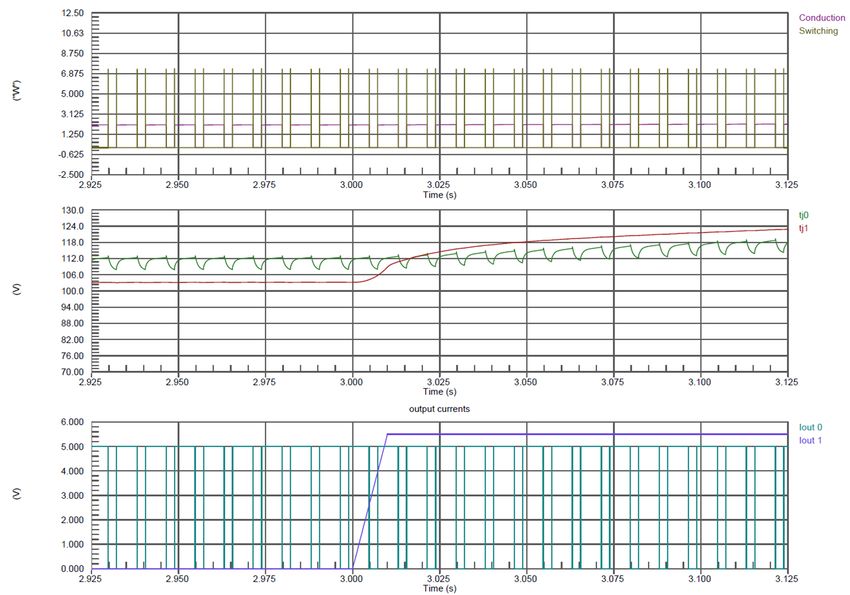
The Figure 12 illustrates a portion of a 10 s simulation. This section illustrates the output 1 transition from off to
on. In this plot two junction temperatures are inserted onto one plot, the two output currents onto one plot and the
two power dissipation components of OUT0 onto one plot. The power dissipation for OUT1 is not shown.
Figure 12. Simulation results
From Figure 12 it can be seen that there are no dramatic thermal excursions. If there were, it would be best to
measure the temperature difference between the junction and the node between R2 and R3 where the quiescent
current power is injected (see Figure 2). From this delta it can be estimated if the device enter power limitation. If
the difference between these two nodes is anything close to 60 °C then it would be advisable to rerun this portion
of the simulation in TwisterSIM. TwisterSIM has a more complex thermal model than what is in the datasheet. The
TwisterSIM model accommodates for the power limitation function more accurately. Using the difference between
the junction (TJx) and node between R2 and R3 as an indicator of power limitation is only an approximation.
If the junction temperature ever exceeds 150 ºC then we can assume that the part can enter thermal shutdown.
The advantage of using SPICE to simulate the thermal response is that it can take less time for longer duration
simulations without affecting accuracy. It can also allow for more complex configurations. It may take less time to
run your simulation in TwisterSIM that it would for you to walk through this lengthy application note and implement
this into your spice simulator. However once done it is available for the next design.
AN5650 - Rev 1 page 16/25AN5650
Code for the simulations shown
Appendix A Code for the simulations shown
The SPICE netlist for Figure 2 generated by Altium (comments in red added by the author) is:
Junction Temperature VND7050AJ 4L with Ron adjust
*SPICE Netlist generated by Advanced Sim server on 1/10/2020 11:55:34 AM
*Schematic Netlist:
* FOSTER Capacitances
C1 TJ0 NetC1_2 0.00035
C2 NetC1_2 NetC2_2 0.005
C3 NetC2_2 NetC3_2 0.05
C4 NetC3_2 NetC4_2 0.4
C5 NetC4_2 NetC5_2 4
C6 NetC5_2 NetC6_2 18
C7 TJ1 NetC7_2 0.00035
C8 NetC7_2 NetC2_2 0.005
*tfall pulse
Ifall_0 Netfall_0_1 TJ0 DC 0 PULSE(0 7.2941 5.965ms 0s 0s 42.5us + 8.33ms) AC 1 0
*initial conditions
.IC V(TJ0)=85V
.IC V(TJ1)=85V
*Load current definitions
ILOAD_Ch0 0 SNS0 DC 0 PULSE(0 5 45us 0s 0s 5.92ms 8.33ms) AC 1 0
ILOAD_Ch1 0 SNS1 DC 0 PWL(0 0 3 0 3.01 6 10 6) AC 1 0
BPdCh0 NetPdCh0_1 TJ0 I=V(SNS0)^2*0.050*(0.8+0.008*V(TJ0))
BPdCh1 0 TJ1 I=V(SNS1)^2*0.05*(0.8+0.008*V(TJ1))
*losses due to the power supply
IPsupply 0 NetC2_2 0.192
*FOSTER resistances
R1 TJ0 NetC1_2 1.8
R2 NetC1_2 NetC2_2 3.2
R3 NetC2_2 NetC3_2 6
R4 NetC3_2 NetC4_2 4
R5 NetC4_2 NetC5_2 3
R6 NetC5_2 NetC6_2 7
R7 TJ1 NetC7_2 1.8
R8 NetC7_2 NetC2_2 3.2
*trise pulse
Irise_0 Netfall_0_1 TJ0 DC 0 PULSE(0 7.3333 0 0s 0s 45us 8.33ms) AC 1 0
*sense resistors for the conduction losses calculators
Rs0 0 SNS0 1
Rs1 0 SNS1 1
*Sense resistors added to measure “power” into the device.
Rsense 0 NetPdCh0_1 0
Rsensesw 0 Netfall_0_1 0
*Ambient temperature setting
VTAmb NetC6_2 0 85V
AN5650 - Rev 1 page 17/25AN5650
Code for the simulations shown
.SAVE 0 NetC1_2 NetC2_2 NetC3_2 NetC4_2 NetC5_2 NetC6_2 NetC7_2 Netfall_0_1
.SAVE NetPdCh0_1 SNS0 SNS1 TJ0 TJ1 Ifall_0[v] ILOAD_Ch0[v] ILOAD_Ch1[v] IPsupply[v]
.SAVE Irise_0[v] VTAmb#branch @VTAmb[z] @C1[i] @C2[i] @C3[i] @C4[i] @C5[i] @C6[i]
.SAVE @C7[i] @C8[i] @R1[i] @R2[i] @R3[i] @R4[i] @R5[i] @R6[i] @R7[i] @R8[i] @Rs0[i]
.SAVE @Rs1[i] @Rsense[i] @Rsensesw[i] @C1[p] @C2[p] @C3[p] @C4[p] @C5[p] @C6[p] @C7[p]
.SAVE @C8[p] @Ifall_0[p] @ILOAD_Ch0[p] @ILOAD_Ch1[p] @IPsupply[p] @Irise_0[p] @R1[p]
.SAVE @R2[p] @R3[p] @R4[p] @R5[p] @R6[p] @R7[p] @R8[p] @Rs0[p] @Rs1[p] @Rsense[p]
.SAVE @Rsensesw[p] @VTAmb[p]
*PLOT TRAN -1 1 A=NetC1_2
*PLOT OP -1 1 A=NetC1_2
*Selected Circuit Analyses: duration and step size of simulation
.TRAN 0.0001666 10 0 0.0001666
.OP
.END
AN5650 - Rev 1 page 18/25AN5650
Alternative RDS(on) equation
Appendix B Alternative RDS(on) equation
There is an alternative RDS(on) equation to the simple linear equation (referencing Equation 1).
The Equation 1 is a linear equation that is fairly accurate for +6σ distribution data and remains within the
specification parameters. This equation is best to use when calculating worst case hot temperature (above 25
°C) analysis. However, a more accurate equation is available for the typical RDS(on) overtemperature. This last
equation provides the typical RDS(on) curve that works over the full temperature range from -40 °C to 150 °C.
Equation 19 – Typical RDS(on) overtemperature
T J + 125 ºC 1.6
RDS on T J = RDS on @ 25 ºC 1 + (19)
300 ºC
For typical RDS(on) over the temperature range, this equation is the best fit.
AN5650 - Rev 1 page 19/25AN5650
Acronyms, abbreviations and reference documents
Appendix C Acronyms, abbreviations and reference documents
Table 5. Acronyms and abbreviations
Terms Description
Conduction losses Power dissipation in a switch while it is on and conducting current into the load
EMI Electromagnetic interference
A thermal modeling method using resistors and capacitors to emulate the dynamic thermal response
Foster model
of a semiconductor
IC Integrated circuit
IPWL A SPICE function that generates a piecewise linear current source
M07 Seventh generation VIPower technology
Piecewise Linear, a line function that describes a line by defining successive points and connecting
PWL
them with straight lines
PWM Pulse width modulation
PWMmed Pulse width modulated
RDS(on) On resistance of an enhanced MOSFET
The rate of change in voltages or current when switching from one state to another (on to off or off to
Slew rate
on)
Open-source software that simulates the operating conditions of analog circuits. It is short for
SPICE
'Simulation Program with Integrated Circuit Emphasis'.
Switching losses Power dissipation in a switch while it is transitioning between off to on or on to off
TwisterSIM Thermal tool made by ST for thermal simulations of ST VIPower products
Vertical Intelligent Power, a semiconductor process developed by ST that is composed of a power
VIPower
MOSFET with embedded control circuitry
Switching energy parameters used to calculate switching losses in ST high side drivers. They
Won, Woff
represent the amount of energy dissipated in a single switching event (on or off)
Table 6. Reference documents
Document name Document type
UM1874 TwisterSIM user manual
AN5368 VIPower M0-7 thermal protections
AN5650 - Rev 1 page 20/25AN5650
Revision history
Table 7. Document revision history
Date Version Changes
19-Apr-2021 1 Initial release.
AN5650 - Rev 1 page 21/25AN5650
Contents
Contents
1 The Foster thermal impedance model . . . . . . . . . . . . . . . . . . . . . . . . . . . . . . . . . . . . . . . . . . . . . . 2
2 Modelling power elements . . . . . . . . . . . . . . . . . . . . . . . . . . . . . . . . . . . . . . . . . . . . . . . . . . . . . . . . . 3
2.1 Initial conditions . . . . . . . . . . . . . . . . . . . . . . . . . . . . . . . . . . . . . . . . . . . . . . . . . . . . . . . . . . . . . . . . 3
2.2 Conduction losses. . . . . . . . . . . . . . . . . . . . . . . . . . . . . . . . . . . . . . . . . . . . . . . . . . . . . . . . . . . . . . 3
2.2.1 Load current definition. . . . . . . . . . . . . . . . . . . . . . . . . . . . . . . . . . . . . . . . . . . . . . . . . . . . . 4
2.2.2 Calculating the conduction losses . . . . . . . . . . . . . . . . . . . . . . . . . . . . . . . . . . . . . . . . . . . . 4
3 Switching losses . . . . . . . . . . . . . . . . . . . . . . . . . . . . . . . . . . . . . . . . . . . . . . . . . . . . . . . . . . . . . . . . . .5
3.1 Switching losses as a DC average . . . . . . . . . . . . . . . . . . . . . . . . . . . . . . . . . . . . . . . . . . . . . . . . 6
3.2 Instantaneous switching losses simulation . . . . . . . . . . . . . . . . . . . . . . . . . . . . . . . . . . . . . . . . . 7
3.2.1 Calculating the output rise and fall times . . . . . . . . . . . . . . . . . . . . . . . . . . . . . . . . . . . . . . . 8
3.2.2 Calculating the energy in each transition. . . . . . . . . . . . . . . . . . . . . . . . . . . . . . . . . . . . . . . 8
4 Clamping inductive energy . . . . . . . . . . . . . . . . . . . . . . . . . . . . . . . . . . . . . . . . . . . . . . . . . . . . . . .10
5 Supply current power dissipation calculations (Psupply) . . . . . . . . . . . . . . . . . . . . . . . . . .13
6 Programming the elements (summary) . . . . . . . . . . . . . . . . . . . . . . . . . . . . . . . . . . . . . . . . . . . .14
6.1 Conduction losses definitions . . . . . . . . . . . . . . . . . . . . . . . . . . . . . . . . . . . . . . . . . . . . . . . . . . . 14
6.1.1 Current definition for conduction losses. . . . . . . . . . . . . . . . . . . . . . . . . . . . . . . . . . . . . . . 14
6.1.2 Power calculations for conduction losses . . . . . . . . . . . . . . . . . . . . . . . . . . . . . . . . . . . . . 14
6.2 Switching losses definitions . . . . . . . . . . . . . . . . . . . . . . . . . . . . . . . . . . . . . . . . . . . . . . . . . . . . . 15
6.2.1 Rise time definitions . . . . . . . . . . . . . . . . . . . . . . . . . . . . . . . . . . . . . . . . . . . . . . . . . . . . . 15
6.2.2 Fall time definitions . . . . . . . . . . . . . . . . . . . . . . . . . . . . . . . . . . . . . . . . . . . . . . . . . . . . . . 15
6.3 Supply current power dissipation definition . . . . . . . . . . . . . . . . . . . . . . . . . . . . . . . . . . . . . . . . 15
7 Reading the results . . . . . . . . . . . . . . . . . . . . . . . . . . . . . . . . . . . . . . . . . . . . . . . . . . . . . . . . . . . . . . .16
Appendix A Code for the simulations shown. . . . . . . . . . . . . . . . . . . . . . . . . . . . . . . . . . . . . . . . . .17
Appendix B Alternative RDS(on) equation . . . . . . . . . . . . . . . . . . . . . . . . . . . . . . . . . . . . . . . . . . . . . .19
Appendix C Acronyms, abbreviations and reference documents . . . . . . . . . . . . . . . . . . . . . .20
Revision history . . . . . . . . . . . . . . . . . . . . . . . . . . . . . . . . . . . . . . . . . . . . . . . . . . . . . . . . . . . . . . . . . . . . . . .21
AN5650 - Rev 1 page 22/25AN5650
List of tables
List of tables
Table 1. Example of a thermal parameter table (VND7050AJ) . . . . . . . . . . . . . . . . . . . . . . . . . . . . . . . . . . . . . . . . . . . 2
Table 2. Switching losses definition (VND7050AJ) . . . . . . . . . . . . . . . . . . . . . . . . . . . . . . . . . . . . . . . . . . . . . . . . . . . 6
Table 3. Switching parameters for the VND7050AJ. . . . . . . . . . . . . . . . . . . . . . . . . . . . . . . . . . . . . . . . . . . . . . . . . . . 8
Table 4. Supply current parameter, IGND(ON) (VND7050AJ) . . . . . . . . . . . . . . . . . . . . . . . . . . . . . . . . . . . . . . . . . . . . 13
Table 5. Acronyms and abbreviations . . . . . . . . . . . . . . . . . . . . . . . . . . . . . . . . . . . . . . . . . . . . . . . . . . . . . . . . . . . 20
Table 6. Reference documents . . . . . . . . . . . . . . . . . . . . . . . . . . . . . . . . . . . . . . . . . . . . . . . . . . . . . . . . . . . . . . . 20
Table 7. Document revision history . . . . . . . . . . . . . . . . . . . . . . . . . . . . . . . . . . . . . . . . . . . . . . . . . . . . . . . . . . . . . 21
AN5650 - Rev 1 page 23/25AN5650
List of figures
List of figures
Figure 1. Six order Foster model equivalent circuit for a 2-channel HSD . . . . . . . . . . . . . . . . . . . . . . . . . . . . . . . . . . . 2
Figure 2. Foster thermal model including power sources . . . . . . . . . . . . . . . . . . . . . . . . . . . . . . . . . . . . . . . . . . . . . . 3
Figure 3. Resistive load switching losses waveform . . . . . . . . . . . . . . . . . . . . . . . . . . . . . . . . . . . . . . . . . . . . . . . . . 5
Figure 4. Typical VIPower M07 high side driver switching waveforms . . . . . . . . . . . . . . . . . . . . . . . . . . . . . . . . . . . . . 5
Figure 5. Inserting average switching power dissipation. . . . . . . . . . . . . . . . . . . . . . . . . . . . . . . . . . . . . . . . . . . . . . . 7
Figure 6. Simulated switching losses. . . . . . . . . . . . . . . . . . . . . . . . . . . . . . . . . . . . . . . . . . . . . . . . . . . . . . . . . . . . 7
Figure 7. Switching and conduction losses simulation results . . . . . . . . . . . . . . . . . . . . . . . . . . . . . . . . . . . . . . . . . . . 7
Figure 8. VND7050AJ maximum turn off energy plot . . . . . . . . . . . . . . . . . . . . . . . . . . . . . . . . . . . . . . . . . . . . . . . . 10
Figure 9. TwisterSIM excessive inductance warning . . . . . . . . . . . . . . . . . . . . . . . . . . . . . . . . . . . . . . . . . . . . . . . . 11
Figure 10. Current flow during inductive clamp . . . . . . . . . . . . . . . . . . . . . . . . . . . . . . . . . . . . . . . . . . . . . . . . . . . . . 11
Figure 11. Inserting the average power dissipation due to clamping . . . . . . . . . . . . . . . . . . . . . . . . . . . . . . . . . . . . . . 12
Figure 12. Simulation results . . . . . . . . . . . . . . . . . . . . . . . . . . . . . . . . . . . . . . . . . . . . . . . . . . . . . . . . . . . . . . . . . 16
AN5650 - Rev 1 page 24/25AN5650
IMPORTANT NOTICE – PLEASE READ CAREFULLY
STMicroelectronics NV and its subsidiaries (“ST”) reserve the right to make changes, corrections, enhancements, modifications, and improvements to ST
products and/or to this document at any time without notice. Purchasers should obtain the latest relevant information on ST products before placing orders. ST
products are sold pursuant to ST’s terms and conditions of sale in place at the time of order acknowledgement.
Purchasers are solely responsible for the choice, selection, and use of ST products and ST assumes no liability for application assistance or the design of
Purchasers’ products.
No license, express or implied, to any intellectual property right is granted by ST herein.
Resale of ST products with provisions different from the information set forth herein shall void any warranty granted by ST for such product.
ST and the ST logo are trademarks of ST. For additional information about ST trademarks, please refer to www.st.com/trademarks. All other product or service
names are the property of their respective owners.
Information in this document supersedes and replaces information previously supplied in any prior versions of this document.
© 2021 STMicroelectronics – All rights reserved
AN5650 - Rev 1 page 25/25You can also read


