Comparative study of atomic force mode and tunneling mode tip-enhanced Raman spectroscopy
←
→
Page content transcription
If your browser does not render page correctly, please read the page content below
Eur. Phys. J. Appl. Phys. 40, 197–201 (2007)
        DOI: 10.1051/epjap:2007144                                                                                                           THE EUROPEAN
                                                                                                                                             PHYSICAL JOURNAL
                                                                                                                                             APPLIED PHYSICS

        Comparative study of atomic force mode and tunneling mode
        tip-enhanced Raman spectroscopy
        G. Picardi1,a , Q. Nguyen1 , J. Schreiber2 , and R. Ossikovski1
        1
            LPICM, École Polytechnique, CNRS, 91128 Palaiseau, France
        2
            HORIBA Jobin Yvon SAS, Raman Division, 231 rue de Lille, 59650 Villeneuve d’Ascq, France
                       Received: 19 July 2007 / Accepted: 22 August 2007
                       Published online: 31 October 2007 –
                                                           c EDP Sciences

                       Abstract. In Tip-Enhanced Raman Spectroscopy (TERS) a metal (or metallized) sharp tip is used to
                       enhance the electromagnetic field by a localized surface-plasmon excitation. Two different modes – atomic
                       force mode (AFM) and scanning tunneling mode (STM) – together with their respective types of probe
                       tips are used in TERS experiments. We have compared the efficiency in enhancing the Raman signal on a
                       thin dye layer for metal-coated AFM tips as well as for electrochemically etched metal STM tips. A much
                       higher enhancement factor and better reproducibility were found when using STM tips. The very different
                       performance is mainly attributed to the more efficient plasmonic excitation when using bulk-metal tips and
                       possibly to the morphological differences in the tip and apex shapes existing between the two tip types.
                       PACS. 07.79.Fc Near-field scanning optical microscopes – 07.79.Lh Atomic force microscopes – 78.30.-j
                       Infrared and Raman spectra – 73.20.Mf Collective excitations

        1 Introduction                                                                           TERS enhancement of up to 106 (enough to attain single
                                                                                                 molecule sensitivity) was reported for a dye layer between
        Raman spectroscopy, an optical characterization tech-                                    a gold tip and a flat gold surface [6,7], while a 14-nm
        nique widely used for chemical and structural analysis,                                  lateral resolution has been reached in Raman imaging of
        is intrinsically limited in spatial resolution to roughly half                           single wall carbon nanotubes [8,9].
        the wavelength of the excitation light, that is, in case of                                  Several factors affect the enhancement observed in the
        UV-Raman, to approximately 150 nm [1]. On the other                                      experiments, such as the tip material, the tip shape, the
        side, scanning probe microscopies (SPM) are preferentially                               nature of the sample substrate underneath the tip, the il-
        used for high resolution surface imaging, routinely show-                                lumination configuration and the tip-sample distance. In
        ing the arrangements of individual molecules or atoms but                                this paper, we present an experimental TERS study com-
        lacking any direct chemical sensitivity.                                                 paring etched metal tips used in STM mode and metal-
             Recently, Raman spectroscopy has been combined                                      coated tips used in AFM contact mode. The comparison
        with either an atomic force microscope (AFM) [2–4] or a                                  was performed on thin dye layer samples deposited on
        scanning tunneling microscope (STM) [5] in a novel tech-                                 a metal surface. In Section 2 the experimental setup, as
        nique called tip enhanced Raman spectroscopy (TERS) or                                   well as the tip and sample preparation procedures, are de-
        scanning near-field Raman spectroscopy. TERS has the                                      scribed. The TERS experimental results are presented in
        premises to perform optical imaging and spectroscopic                                    Section 3 and discussed in Section 4, by analyzing criti-
        analysis with sub-diffraction limited resolution. Within                                  cally the possible factors influencing the observed signal
        this approach, a nanometer-sized metal (Au or Ag) object,                                enhancement, such as tip material and geometry.
        i.e. the end apex of a probe tip, is placed inside the laser
        spot. By acting as a local antenna, the tip enhances by sev-
        eral orders of magnitude the incident electromagnetic field
        in its close surrounding. Only molecules located within the
                                                                                                 2 Experimental
        near field of the enhancing tip are affected and thus probed
        by TERS. The field enhancement stems from a combina-                                      A high resolution Raman spectrometer (HR800 from
        tion of the electrostatic lightning rod effect and the excita-                            HORIBA Jobin Yvon) is coupled to an AFM micro-
        tion of Localized Surface Plasmons (LSP) at the tip apex.                                scope (XE-100 from PSIA) through a home-made opto-
        TERS has potentially a wide range of applications: from                                  mechanical coupling system (Fig. 1). The system con-
        materials nano-characterization in the semiconductor in-                                 sists of three mirrors, four manual translational stages
        dustry to single molecule studies in the biological field. A                              and a long working-distance objective (50×, NA = 0.45
                                                                                                 from Olympus) oriented at 70◦ with respect to the sam-
            a
                e-mail: gennaro.picardi@polytechnique.edu                                        ple normal. The same objective is used for backscattering

        Article published by EDP Sciences and available at http://www.edpsciences.org/epjap or http://dx.doi.org/10.1051/epjap:2007144

Downloaded from https://www.cambridge.org/core. IP address: 46.4.80.155, on 24 Nov 2020 at 06:28:23, subject to the Cambridge Core terms of use, available at https://www.cambridge.org/core/terms
. https://doi.org/10.1051/epjap:2007144
198 The European Physical Journal Applied Physics
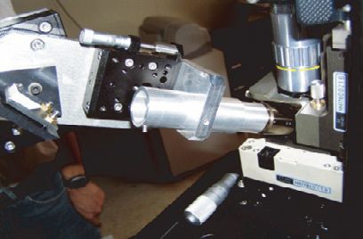
Fig. 1. Schematics of the TERS set-up. A picture of the 70◦ -tilted Raman objective and the AFM microscope sample holder
is given in the insert.
collection of the Raman radiation. The XE-100 head has the help of the oblique view from the spectrometer cam-
been modified (see insert in Fig. 1) in order to allow for era and the translational stages. A “tip-enhanced” Raman
the close approach of the objective to the tip-sample re- spectrum was then collected with the tip engaged. The
gion. The system supports both AFM and STM operat- tip was subsequently retracted at a distance of several µm
ing modes by changing the corresponding tip support. A while maintaining the laser alignment and a second spec-
633-nm-wavelength He-Ne laser beam (p-polarization) is trum was recorded. The above procedure may be repeated
focused to the tip apex and aligned through the microme- several times on the same or on another sample point as
ter stages. Laser power was kept below 1 mW in order to a reproducibility check.
avoid sample heating and possible tip apex deterioration.
Commercially available AFM (from Veeco, Mikro-
masch, Nanosensors) tips were coated by thermal evapo- 3 Results
ration with a 10-nm adhesive Cr layer followed by a 20- In a TERS experiment, the observed contrast C is defined
to 40-nm Au coating (evaporation speed: 0.2–0.1 nm/s). as the ratio of the Raman scattered intensity (for a specific
STM tips were prepared by electrochemical etching of a band) with the tip engaged and the tip withdrawn:
0.25-mm Au wire (from Goodfellow ) in a concentrated
HCl/ethanol 1:1 mixture. Tips with final apex radii lower C = Itip engaged /Itip withdrawn . (1)
than 30 nm can be reproducibly prepared in this way [10, This ratio can be used as a measure of the ability of a
11]. A home made circuit automatically switches off the TERS experiment to discriminate the contribution to the
etching current as soon as the lower portion of the wire signal due to the tip enhancement from that coming from
detaches. Figures 2a and 2b show scanning electron mi- the entire illuminated surface. Figures 3a and 3b show
croscope (SEM) pictures of an AFM and an STM tip, typical Raman spectra of the BCB dye layer with and
respectively. without the presence of the tip, in AFM and STM modes
A dye layer was deposited on an Au-coated substrate respectively. A maximum contrast of 1.4 (at 585 cm−1 )
by casting a single drop from a 10−6 M Brilliant Cresyl was found in AFM mode while contrast values ranging
Blue (BCB) solution in ethanol and subsequent rinsing in from 20 up to 100 (depending on the tip-to-tip perfor-
the pure solvent in order to remove any excess material mance variation) were observed in STM mode. (The steep
and to have only a molecular layer adsorbed on the metal background increase observed in the “red” region of the
surface. The Au-coated substrate is essential for fluores- Figure 3a spectrum is due to a stray light contribution
cence quenching and for the tunneling feedback control from the red diode laser used for the AFM mode optical
in the STM operating mode. Flame-annealed atomically feedback.)
smooth Au(111) surfaces (from Arrandee) and a 60-nm Because of the substantially lower contrast values ob-
evaporated Au layer on glass were used, for STM and tained in AFM mode compared to STM mode ones,
AFM mode measurements, respectively. the tip-withdrawn-spectrum response in the AFM exper-
In each experiment, two Raman spectra were acquired iments was intentionally “boosted” by using an evapo-
in the following sequence: the tip was first approached to rated Au substrate presenting a granular roughness (about
the sample (in STM current-feedback mode or in AFM 2 nm rms) and consequently supporting some surface en-
contact mode with, respectively, 1–0.5 nA tunneling cur- hanced Raman (SERS) effect. By using a “mildly” ac-
rent at 0.1 V and 1–5 nN contact force) and the laser tivated SERS substrate it is thus possible to make visi-
spot was focused onto the tip – sample contact point with ble even a very small signal enhancement due to the tip,
Downloaded from https://www.cambridge.org/core. IP address: 46.4.80.155, on 24 Nov 2020 at 06:28:23, subject to the Cambridge Core terms of use, available at https://www.cambridge.org/core/terms
. https://doi.org/10.1051/epjap:2007144G. Picardi et al.: Comparative study of atomic force mode and tunneling mode tip-enhanced Raman spectroscopy 199
Fig. 2. SEM pictures of (a) an Au-coated AFM tip (top view)
and (b) an etched-Au wire STM tip (side view). The flake at
the STM tip apex results from carbon contamination from the Fig. 3. Tip enhanced Raman spectra of a BCB dye layer de-
vacuum pump. posited on metal surface recorded in AFM and STM modes.
Lower trace corresponds to the tip withdrawn, the upper trace
– to the tip engaged. (a) Au-coated AFM tip operating on a
as is the case in Figure 3b. In contrast to the AFM tip dye-covered evaporated Au film. Acquisition time: 10 s. Laser
experiments, in the experiments with the STM etched power: 0.5 mW. (b) Etched-Au STM tip operating on a dye-
tips the atomically smooth Au surface supports almost no covered atomically smooth Au film. Acquisition time: 20 s.
Laser power: 0.5 mW.
SERS effect and the “tip engaged” spectrum is practically
flat while the “tip-enhanced” spectrum is still remarkably
high, see Figure 3b. AFM tips previously tested on these
atomically smooth substrates were not able to provide any An approximate estimation of the Raman signal en-
appreciable signal enhancement. hancement factor (EF ) can be performed by assuming
The difference in enhancement performance between that the difference in signal intensities between the “tip
STM and AFM tips is accompanied by a similar difference engaged” spectrum and the “tip withdrawn” spectrum is
in enhancement reproducibility. TERS spectra recorded mainly due to those molecules of the sample that are clos-
in STM mode showed quite different contrast values (ow- est to the tip apex since the enhanced (or near) field gener-
ing to the tip-to-tip variation), but for almost all of the ated by the plasmon excitation at the tip apex decays very
tested tips a clear Raman spectra exhibiting the dye vi- rapidly with moving away from the tip. Within the sim-
brational fingerprints was recorded in tip-engaged posi- plest configurational approximation, the tip enhanced sig-
tion. On the contrary, despite testing different kinds of nal comes from a circular area with radius comparable to
commercial AFM tips as well as slightly varying the evap- the tip apex radius. In this case the enhanced field can be
oration procedure conditions (metal film thickness, evap- considered to be constant over a circle, although different
oration speed, angle of the cantilever with respect to the and more realistic field distributions below the tip apex
crucible), a signal enhancement was observed only for a have been taken in account by Pettinger et al. [12]. There-
small number of AFM tips (about 20 percent). fore, the EF can be calculated from the experimental C
Downloaded from https://www.cambridge.org/core. IP address: 46.4.80.155, on 24 Nov 2020 at 06:28:23, subject to the Cambridge Core terms of use, available at https://www.cambridge.org/core/terms
. https://doi.org/10.1051/epjap:2007144200 The European Physical Journal Applied Physics
values by normalizing the signals by the corresponding a half sphere (or a half ellipsoid). A “nano-star” [15] ap-
laser illuminated (or focal) area A and by the TERS cir- pears as a more adequate description of the apex surface
cular area presenting a number of protusions that (cooperatively)
support plasmon excitation.
C = 1+EF (Stip engaged /Stip withdrawn ) = 1+EF (πrtip2
/A). Regarding other differences between the two kinds of
(2) tips, it can be readily found either from the SEM pic-
As a direct consequence of the oblique incidence, the laser tures or from the microscope side view that the STM tips
beam forms an elliptical spot on the sample with major present a smaller aperture angle (G. Picardi et al.: Comparative study of atomic force mode and tunneling mode tip-enhanced Raman spectroscopy 201
in shear-force feedback mode [23,24]. Different tip-coating 6. B. Pettinger, B. Ren, G. Picardi, R. Schuster, G. Ertl,
procedures exist [25] and the possibility to further refine Phys. Rev. Lett. 92, 096101 (2004)
the tip shape by ion milling can also be considered. How- 7. K.F. Domke, D. Zhang, B. Pettinger, J. Am. Chem. Soc.
ever, these preparation methods become less straigthfor- 128, 14721 (2006)
ward and, once again, the general reproducibility has still 8. A. Hartschuh, E.J. Sanchez, X. Sunney Xie, L. Novotny,
to be demonstrated. Phys. Rev. Lett. 90, 095503 (2003)
9. N. Anderson, A. Hartschuh, S. Cronin, L. Novotny, J. Am.
Chem. Soc. 127, 2533 (2005)
10. B. Ren, G. Picardi, B. Pettinger, Rev. Sci. Instrum. 75,
5 Conclusions 837 (2004)
11. L. Billot, L. Berguiga, M. Lamy de la Chapelle, Y. Gilbert,
We presented a comparative study of two commonly used R. Bachelot, Eur. Phys. J. Appl. Phys. 31, 139 (2005)
TERS experimental approaches: using metal-coated tips 12. B. Pettinger, B. Ren, G. Picardi, R. Schuster, G. Ertl, J.
in AFM contact mode and using etched-metal tips in STM Raman Spectrosc. 36, 541 (2005)
mode. The experimental results on a dye layer deposited 13. T. Schmid, T.A. Schmitz, P.D. Setz, B.S. Yeo, W. Zhang,
on a metal film indicate a much stronger TERS effect R. Zenobi, Chimia 60, (2006)
and overall better reproducibility when using metal-etched 14. B.S. Yeo, T. Schmid, W. Zhang, R. Zenobi, Anal. Bioanal.
STM tips. Possible reasons for this observation, such as Chem. 387, 2655 (2007)
the intrinsically lower “optical quality” of the coated tips 15. F. Hao, C.L. Nehl, J.H. Hafner, P. Nordlander, Nano Lett.
with respect to the massive metal ones as well as the dif- 7, 729 (2007)
ferences in tip shapes, have been discussed. We believe 16. C. Georgi, M. Hecker, E. Zschech, Appl. Phys. Lett. 90,
that this study may prove helpful when planning a TERS 171102 (2007)
experiment. 17. R.W. Rendell, D.J. Scalapino, Phys. Rev. B 24, 3276
(1981)
18. J.A. Porto, P. Johansson, S.P. Apell, T.L. Lopez-Rios,
One of the authors (Q. Nguyen) gratefully recognizes a CIFRE Phys. Rev. B 67, 085409 (2003)
PhD scholarship by Ecole Polytechnique and HORIBA Jobin 19. K. Meguro, K. Sakamoto, R. Arafune, M. Satoh, S.
Yvon. Ushioda, Phys. Rev. B 65, 165405 (2002)
20. A. Cvitkovic, N. Ocelic, J. Aizpurua, R. Guckenberger, R.
Hillenbrand, Phys. Rev. Lett. 97, 060801 (2006)
21. W. Zhang, X. Cui, B.S. Yeo, T. Schmid, C. Hafner, R.
Zenobi, Nano Lett. 7, 1401 (2007)
References 22. It is to be stressed again that better TERS performance
is observed on metallic substrates whatever the operating
1. V. Poborchii, T. Tada, T. Kanayama, Appl. Phys. Lett. mode (AFM or STM)
89, 233505 (2006) 23. C.C. Neacsu, J. Dreyer, N. Behr, M.B. Raschke, Phys. Rev.
2. R.M. Stoeckle, Y.D. Suh, V. Deckert, R. Zenobi, Chem. B 73, 193406 (2006)
Phys. Lett. 318, 131 (2000) 24. N. Anderson, A. Hartschuh, L. Novotny, Nano Lett. 7, 577
3. M.S. Anderson, Appl. Phys. Lett. 76, 3130 (2000) (2007)
4. N. Hayazawa, A. Tarun, Y. Inouye, S. Kawata, J. Appl. 25. J.J. Wang, Y. Saito, D.N. Batchelder, J. Kirkham, C.
Phys. 92, 6983 (2002) Robinson, D.A. Smith, Appl. Phys. Lett. 86, 263111
5. B. Pettinger, G. Picardi, R. Schuster, G. Ertl, Single Mol. (2005)
3, 285 (2002)
Downloaded from https://www.cambridge.org/core. IP address: 46.4.80.155, on 24 Nov 2020 at 06:28:23, subject to the Cambridge Core terms of use, available at https://www.cambridge.org/core/terms
. https://doi.org/10.1051/epjap:2007144You can also read