DESIGN WIN FOR SMARTPHONE: THE STRATEGIC CHOICES MADE BY SAMSUNG, APPLE, XIAOMI
←
→
Page content transcription
If your browser does not render page correctly, please read the page content below
Press Release
April 28th, 2021
LYON, France
DESIGN WIN FOR SMARTPHONE:
THE STRATEGIC CHOICES MADE BY
SAMSUNG, APPLE, XIAOMI…
Smartphone Design Win Quarterly Monitor – Q1, 2021
Q1 2021 TECHNICAL DYNAMICS :
• Design wins:
o System Plus Consulting announces an average of 188 chips per smartphone,
against 176 chips in Q4 2020.
o Top 3 vendors: this period shows Qualcomm leading the market with 17% of
the total design wins. Then after, we see Qorvo and Murata.
o USA dominates the market with 47% design wins. Japan and China are following.
• eBoM :1
o Memory represents 28% of eBoM cost in Q1 2021.
o NAND & DRAM drive the cost, with only 4 players involved: Samsung, Kioxia,
SK Hynix and Micron.
• Die area:
o The total die area in Q1 2021 reaches 10,339 mm².
o The market is mainly dominated by two countries, USA and Korea with more
than 76% market shares2.
o Samsung is leading the die area utilization in Q1 2021, with 30% of the total die
area.
o Without doubt, memory is the main driver.
o Memory accounts for 4,262 mm² of dies area in Q1 2021
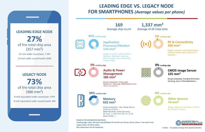
LEADING-EDGE TECHNOLOGIES AND TECHNOLOGY NODES
Huge investments worldwide from the likes of TSMC and SK Hynix, underpin this technology
node right now, making this metric one to watch. “We've all heard about the buzz in Europe, the
US, Taiwan and South Korea surrounding investments to establish a supply chain for these leading-
edge technologies,” asserts Romain Fraux, CEO of System Plus Consulting. “In this
context, it's really important to track how these technology nodes are being used in the smartphones
industry.”
Technology nodes of 14 nm down to 5 nm represent 27% of die area in devices. Importantly,
around 1.9 million units of 12-inch wafers are shipped per quarter using these technology
1
eBoM: Engineering Bill of Material
2
Based on the die area in mm²
Press Release
nodes. Meanwhile some 2.2 million and 1.0 million units of 12-inch wafers are shipped with
the legacy 28-16 nm and 90-32 nm nodes per quarter, respectively.
“You won't see a metric like this anywhere else,” highlights Fraux. “For silicon wafer manufacturers,
for example, this is so important as you can understand your market in terms of wafer size, technology
and other segments.”

COMPONENT, PACKAGING AND SILICON CHIP: WHAT ARE THE
TECHNICAL CHOICES MADE BY SAMSUNG, APPLE…?
Electronic costing and technology experts at System Plus Consulting have released the
Smartphone Design Win Monitor which provides unique industry insight into the latest
component, packaging and silicon chip choices of smartphone makers.
Much of the detail is based on teardowns from System Plus Consulting, which uncover the
innovative design features and new semiconductor components within a smartphone. “You can
often find some online data on, say, chipset providers, but this will only provide a small part of the
entire picture,” says Romain Fraux. “With our quarterly Smartphone Design Win Monitor, we are
providing an exhaustive view of the content of the smartphones we've analysed in terms of technology
choice, based on our many tear-downs.”

THE US AREA HAS CAPTURED A MIGHTY 47% OF DESIGN WINS
Each Smartphone Design Win Monitor looks at 8 representative handsets per quarter, tracking
the shipment market share – so if one vendor has 20% market share then around 20% of the
phones analysed will come from that vendor.
“The Monitor includes a database with historical and latest information, providing a one-year view so
readers can understand trends on an annual basis,” explains Audrey Lahrach, Technology &
Cost Analyst, deeply involved in the development of the Smartphone Design Win
Monitor at System Plus Consulting. Detail is provided on the phone and IC3 manufacturer
with, for example, data and graphs illustrating the design wins per vendor from quarter to

3
    IC: Integrated Circuit

                                                                                                    2
Press Release
quarter. Indeed, in the most recent quarterly update, Qualcomm has a clear lead on design
wins, followed by Qorvo and Murata.
Likewise, data on design wins per nationality - which represents the country of a company's
headquarters - are provided. Latest figures reveal how the US has captured a mighty 47% of
design wins, a figure that had changed very little from the previous quarter.
Data is also provided on package footprint per vendor, category and packaging technology.
For example, in the latest Monitor, Qualcomm and Samsung are leading the pack on footprint
but huge variations are seen from quarter to quarter.
In a similar vein, recent data on electronic bill of materials - eBoM - reveals that, at least for
now, memory is driving the cost of phones, with 28% in Q1 2021 against 34% in Q4 2020.
This excludes display, battery, PCB4 and mechanical components.
In addition, data on die, wafer and technology indicates that Samsung - a key provider of
memory chips - now leads die area utilization, with 3,123 mm2 (30%).
More information in the dedicated article: Smartphone Design Win Monitor : discover the
decisions that global manufacturers make article.
System Plus Consulting’s Smartphone Design Win Monitor will be
published every beginning of March (Q1), June (Q2), September (Q3)
and December (Q4)...
Targeting financial investors, device maker marketing teams, companies
involved in the supply chain for equipment, packaging, materials and
more, the quarterly update offers a clear view of the semiconductor companies leading this rapidly
growing market, drawing comparisons between OEM5s and including easily digestible information on
the supply chain and technology evolution. This smartphone monitor utilizes data from representative
phones (65+ phones per year torn down in the System Plus Consulting Phone Teardown Track
Module).
Stay tuned on reverse-costing.com to get further information about our activities!
System Plus Consulting is partner with Yole Développement (Yole), both part of Yole Group of
Companies.
Press contacts for Yole Group
Sandrine Leroy, Director, Public Relations, sandrine.leroy@yole.fr
Marion Barrier, Assistant, Public Relations, marion.barrier@yole.fr
www.yole.fr - www.reverse-costing.com – LinkedIn – Twitter
4
PCB: Printed Circuit Board
5
OEM: Original Equipment Manufacturer
3Press Release
About the authors
Romain Fraux is the CEO of System Plus Consulting, part of our Yole Group of companies. System Plus
Consulting’s activities are dedicated to reverse costing analyses of electronics, from semiconductor devices to
electronic systems. Supporting industrial companies in their development, Romain and his team are offering a
complete range of services, costing tools and reports. They deliver in-depth production cost studies and estimate
objective selling price of a product, all based on a detailed physical analysis of each component in System Plus
Consulting laboratory. Romain has been working for System Plus Consulting for more than 15 years and was
previously the company’s CTO. He holds a bachelor’s degree in Electrical Engineering from Heriot-Watt
University of Edinburgh (Scotland), a master’s degree in Microelectronics from the University of Nantes (France),
and a Master of Business Administration.
Audrey Lahrach serves as a Technology & Cost Analyst, MEMS, Sensors & Display at System Plus Consulting,
part of Yole Développement. With significant expertise in the field of MEMS & sensors, including inertial, pressure
and gas, as well as in the field of display technologies, Audrey produces reverse engineering & costing analyses
while also running custom projects. Her mission is performed in collaboration with the laboratory team, and
together they define the objectives of the analyses and determine the methodologies to reveal the structure of
the devices and all materials required for their development and production. Audrey's aim is to determine and
understand the technology choices made by the leading sensing companies, from the materials to the device itself.
Thanks to her previous experience with CMOS image sensors and camera manufacturing, Audrey is also involved
in the development of System Plus Consulting’s imaging activities. Audrey holds a master’s degree in
Microelectronics from the University of Nantes (France).
About System Plus Consulting
System Plus Consulting specializes in the cost analysis of electronics, from semiconductor devices to electronic
systems. Created more than 20 years ago, System Plus Consulting has developed a complete range of services,
costing tools and reports to deliver in-depth production cost studies and estimate the objective selling price of
a product… More
For more information and images, please visit www.reverse-costing.com
###
4You can also read