DesignCon 2018 16Gb/s and Beyond with Single-Ended I/O in High-Performance Graphics Memory
←
→
Page content transcription
If your browser does not render page correctly, please read the page content below
DesignCon 2018
16Gb/s and Beyond with Single-
Ended I/O in High-Performance
Graphics Memory
Tim Hollis, Micron Technology, Inc.
[Email: thollis@micron.com]
Salman Jiva, Micron Semiconductor Products
Martin Brox, Micron Semiconductor GmbH
Wolfgang Spirkl, Micron Semiconductor GmbH
Thomas Hein, Micron Semiconductor GmbH
Dave Ovard, Micron Technology, Inc.
Roy Greeff, Micron Technology, Inc.
Dan Lin, Micron Technology, Inc.
Michael Richter, Micron Semiconductor GmbH
Peter Mayer, Micron Semiconductor GmbH
Walt Moden, Micron Technology, Inc.
Maksim Kuzmenka, Micron Semiconductor GmbH
Mani Balakrishnan, Micron Semiconductor GmbH
Milena Ivanov, Micron Semiconductor GmbH
Manfred Plan, Micron Semiconductor GmbH
Marcos Alvarez Gonzalez, Micron Semiconductor GmbH
Bryce Gardiner, Micron Technology, Inc.
Dong Soon Lim, Micron Technology, Inc.
Jörg Weller, Micron Semiconductor GmbH
                                                                1
©2018 Micron Technology, Inc. All rights reserved. Information, products, and/or specifications are subject to change without
notice. All information is provided on an “AS IS” basis without warranties of any kind. Drawings may not be to scale. Micron, the
Micron logo, and all other Micron trademarks are the property of Micron Technology, Inc. All other trademarks are the property of
their respective owners. Rev. A, 01/18 CCM004‐676576390‐10965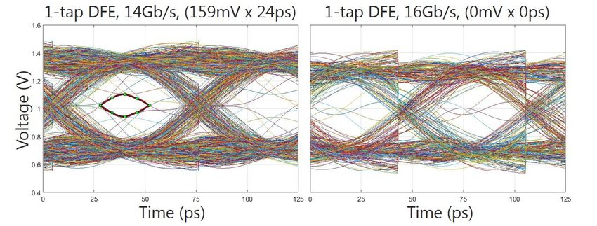
Abstract
GDDR5 has emerged as a leading DRAM interface for applications requiring high
system bandwidth like graphic cards, game consoles and high-performance compute
systems. However, the requirements of newer applications drive even higher memory
bandwidth. The paper discusses the development of GDDR6 as a lower-risk and more
cost-effective solution as compared to other high-bandwidth memory solutions. We
further introduce GDDR6 as offering a 2x increase in per-pin bandwidth over GDDR5,
while maintaining compatibility with the established GDDR5 ecosystem. Circuit and
channel performance scaling will be discussed and validated through measurement to
demonstrate the potential for scaling GDDR6 to 16Gb/s.

Authors Biography

Tim Hollis received the B.S. degree in Electrical Engineering from the University of
Utah, Salt Lake City, UT in 2003 and the Ph.D. in Electrical Engineering from Brigham
Young University, Provo, UT in 2007, focusing on channel equalization and jitter
attenuation circuits for high-speed serial interconnects. He joined Micron Technology,
Inc.’s Advanced Architecture Group in 2006 and currently serves as the Technical Lead
for Micron Technology, Inc.’s Signal Integrity R&D team, focusing on future I/O
development. Dr. Hollis holds 122 issued US and International patents and is a Senior
Member of the IEEE.

Salman Jiva is a segment marketing and business development manager for Micron
Technology, Inc.’s Compute and Networking Business Unit. He leads the product and
customer strategy efforts for Micron Technology, Inc.’s networking segment and partners
with Micron Technology, Inc.’s ecosystem to enable technologies with key
semiconductor and system partners. Before coming to Micron Technology, Inc., Salman
spent over seven years at Altera Corporation, where he held several positions in product
management, product marketing and technical marketing for their high end FPGAs, SoCs
and respective technologies. Salman also spent 6 years at Cisco Systems as a hardware
and systems engineer designing enterprise class switches and routers. Mr. Jiva earned his
M.S degree in electrical engineering from Santa Clara University.

Martin Brox received Dipl. and Dr. degrees from the University Münster in 1988 and
1992 respectively. In 1988 he joined Siemens Corporate Research and in 1992 moved to
the IBM/Siemens/Toshiba DRAM development project. In 1997 he returned to
Siemens/Munich which later became Infineon and Qimonda responsible for RDRAM,
GDDR3 and GDDR5. In 2009 he joined Elpida (now part of Micron Technology, Inc.)
focusing on GDDR5, GDDR5X and GDDR6. Dr. Brox served on the program committee
of ISSCC and is serving on ESSCIRC/ESSDERC.
                                                                2
©2018 Micron Technology, Inc. All rights reserved. Information, products, and/or specifications are subject to change without
notice. All information is provided on an “AS IS” basis without warranties of any kind. Drawings may not be to scale. Micron, the
Micron logo, and all other Micron trademarks are the property of Micron Technology, Inc. All other trademarks are the property of
their respective owners. Rev. A, 01/18 CCM004‐676576390‐10965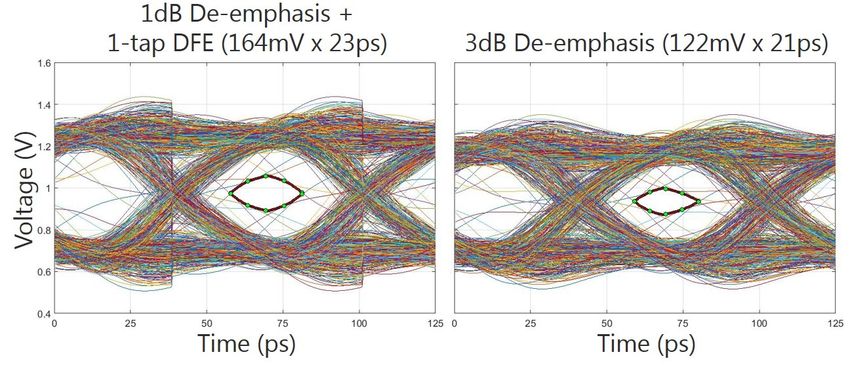
Wolfgang Spirkl received a diploma degree in Physics from the Ludwig-Maximilians-
University (LMU, Munich, Germany) in 1986, and a Ph.D. degree in Physics as well from
the LMU in 1990. From 1998 on he worked for Siemens (later Infineon, Qimonda) in the
verification of embedded, network, commodity and graphic DRAM. He is currently
working in the Micron Technology, Inc.’s Munich Design Centre on product and test for
high speed graphic DRAM.

Thomas Hein received the Diploma in information technology from the Technical
University of Dresden in 1995. In 1995 he joined Siemens Semiconductors, which
became Infineon Technologies and later Qimonda AG, where he led the design of
multiple Multi-Bank MDRAM, SGRAM, GDDR1/3/4/5 designs. From 2009 to 2014 he
worked for Elpida Memory (Europe) GmbH. In 2014, he joined Micron Semiconductor
(Deutschland) GmbH where he currently working on definition and design and of various
high-speed GDDR5, GDDR5X and GDDR6 DRAMs. He was the design lead of the 8G
GDDR5X. His interests in DRAM design includes new DRAM architectures, chip
packaging and high-speed interfaces.

Dave Ovard received a B.S. degree in electrical engineering from the University of Utah
(Salt Lake City, Utah USA) in 1987. He has been a member of the Signal Integrity R&D
Group at Micron Technology, Inc. (Boise, Idaho USA) since 1999. Prior to joining
Micron Technology, Inc., he worked at Unisys, developing military data links;
Omnipoint Communications, developing early CDMA cell phone technology; and
Micron Communications, developing RFID technology. Mr. Ovard is a member of the
IEEE and holds more than 60 patents.

Roy Greeff received a B.S. degree in electrical engineering from the University of Utah
(Salt Lake City, Utah USA) in 1978. Presently he works at Micron Technology, Inc.
(Boise, Idaho USA) as a Senior Signal Integrity Engineer. Previously he worked as
Microwave Communications Engineer in the defense industry. Mr. Greeff has more than
40 patents.

Feng (Dan) Lin received the Ph.D. degree in Electrical Engineering (EE) from the
University of Idaho, Boise, ID in 2000, and M.S. and B.S. degrees in EE from the
University of Electrical Science and Technology of China in 1995 and 1992 respectively.
He joined DRAM Design R&D at Micron Technology, Inc., Boise in 2000, focusing on
the development of high-speed, leading edge DRAM for high-performance computing.
He most recently serves as the lead designer in Signal Integrity R&D team for advanced
memory architecture and future I/O development. Dr. Lin is a co-author of the textbook
DRAM Circuit Design, Fundamental and High-Speed Topics (Wiley-IEEE Press, 2008).
Dr. Lin holds over 117 U.S. and foreign patents to date.

                                                                3
©2018 Micron Technology, Inc. All rights reserved. Information, products, and/or specifications are subject to change without
notice. All information is provided on an “AS IS” basis without warranties of any kind. Drawings may not be to scale. Micron, the
Micron logo, and all other Micron trademarks are the property of Micron Technology, Inc. All other trademarks are the property of
their respective owners. Rev. A, 01/18 CCM004‐676576390‐10965
Michael Richter received a diploma in electrical engineering from the Technical
University Munich (Munich, Germany) in 1982. He joined Siemens Semiconductors in
1984 where his work included ASIC design and design support for ASIC customers.
Later, he joined Infineon Technologies AG where he served as a Program Manager of a
high-speed crypto IC project. With Qimonda AG he was responsible for product
definition and standardization of GDDR5, which he continued with Elpida Memory and
now with Micron Technology, Inc. on GDDR5X and GDDR6.

Peter Mayer made a professional training as radio and TV technician and received a
Diploma in electrical engineering from the University of Erlangen (Germany) in 1997. In
1997 he joined Siemens Semiconductor in Munich which became Infineon Technologies
and later Qimonda. There he served in product engineering team and lead graphics
memory (SGRAM, GDDR1 to GDDR5) system team. In 2009 the graphics group joined
Elpida (now Micron Technology, Inc.), where he works on GDDR5, GDDR5x and
GDDR6 system enabling, system design analysis and technical customer support. He is
author or co-author of several US and international patents.

Walter Moden received a B.S. and 2 M.S. degrees from the University of Idaho
(Moscow, ID) in 1984, 1986, and 1989. He has been at Micron Technology, Inc. (Boise,
Idaho USA) since 1988, holding various positions in the Assembly and Packaging
Groups. Currently working as a Principle Package Design Engineer focusing on high
speed memory. Mr. Moden holds over 140 U.S. and foreign patents.

Maksim Kuzmenka received a diploma in electronics from the Belarusian State
University of Informatics and Electronic (Minsk, Belarus) in 1993. In 1993, he joined
BELOMO (Belarusian Optic-Mechanics Association) where he worked in the area of
pulse mode power supplies design. In 2001, he joined the Memory Products division of
Infineon Technologies which was later changed to Qimonda and Elpida (now Micron
Technology, Inc.). He participated in the development of IO and multiple other analog
and mixed mode circuitry. Mr. Kuzmenka is the (co-)author of several European and U.S.
patents

Mani Balakrishnan received a B.S. degree from the Coimbatore Institute of Technology
(Coimbatore, India) in 2000 and an M.S. degree from the University of Southern
California (Los Angeles, California USA) in 2003. He worked with Biomorphic from
2004 to 2006 in CMOS Image Sensor and Intel India from 2006 to 2012 in Design and
Development of High-speed IO blocks for the Intel Architecture Group. In 2013, he
joined Elpida (now Micron Technology, Inc.). He is working on High-speed PLL and
Receiver Blocks.

Milena Ivanov received Master degree in telecommunications from the Technical
University in Sofia, Bulgaria, in 1996, and the Diploma in electrical engineering from the
                                                                4
©2018 Micron Technology, Inc. All rights reserved. Information, products, and/or specifications are subject to change without
notice. All information is provided on an “AS IS” basis without warranties of any kind. Drawings may not be to scale. Micron, the
Micron logo, and all other Micron trademarks are the property of Micron Technology, Inc. All other trademarks are the property of
their respective owners. Rev. A, 01/18 CCM004‐676576390‐10965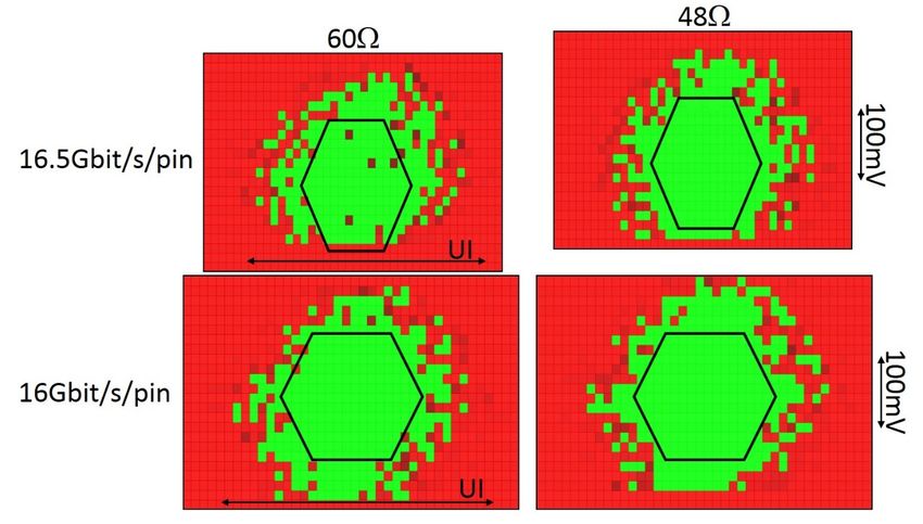
Technical University of Munich, Germany in 2005. She joined the Memory Products
Division of Infineon Technologies (which became Qimonda AG) in 2005 and was active
in the development of emerging memories, in particular, conductive bridging RAM. In
2009 she joined Elpida (now Micron Technology, Inc.) and was engaged in the
development of GDDR5, GDDR5X and GDDR6. Ms. Ivanov is author as well as co-
author of several US-patents.

Manfred Plan received a diploma in electrical engineering from the Technical
University of Munich (Munich, Germany) in 1987. In 1988, he joined Siemens AG,
received admission to a trainee program (Siemens Graduate Program), and worked in
different product development divisions (Berkeley, California USA and Villach, Austria).
From 1990 until 1998, he was active in chip and memory design for the Consumer
Development division and until 2000 in microprocessor design for the Chipcard
Development division at Siemens/ Infineon AG. In 2000, he moved to the Memory
Product Development division at Infineon/Qimonda AG where he worked on embedded
DRAM, RLDRAM, and GDDR5 until 2009, and he then joined Elpida (now Micron
Technology, Inc.). Mr. Plan is a member of FEANI, co-author of several publications,
and holds some national patents as well as one U.S. patent.

Marcos Alvarez Gonzalez received a B.S. and M.S. degree in computer science and
engineering from the Universidad de A Corunna (Spain) in 2008 and a M.S. degree in
computer science and artificial intelligence from Arizona State University (USA) in
2010. He joined Micron Technology, Inc. (Boise, ID, USA) in 2010 as a quality and
reliability assurance engineer. In 2015 he started working for Micron Semiconductor
Deutschland (Munich, Germany) as a senior product engineer.

Bryce Gardiner received a BS degree in electrical engineering, from the University of
Utah, Salt Lake City, Utah in 2009. He is currently a Senior Signal Integrity Engineer in
the Systems Signal Integrity group at Micron Technology, Inc. (Boise, ID USA). His
current work at Micron Technology, Inc. is in providing power and signal integrity
analysis by optimizing test boards, characterization boards and systems across Micron
Technology, Inc.’s entire product portfolio. Before joining Micron Technology, Inc. in
2010, he worked for Northrop Grumman in their Electronic Navigation Systems
Division, developing Electronic Guidance Systems. Mr. Gardiner is a member of IEEE.

Dong Soon Lim received a B.S. degree in electrical engineering from the University of
Dong-A (Busan, Korea) in 1996. He is working as a senior signal integrity engineer at
Micron Technology, Inc. (Boise, Idaho USA). He is responsible for the electrical models,
substrate design optimization, SI and PI performance of high speed memory packages.
His interests include high speed package design and system level analysis for high-speed
products, such as LPDDR4 and graphic DRAM. Before joining Micron Technology, Inc.,

                                                                5
©2018 Micron Technology, Inc. All rights reserved. Information, products, and/or specifications are subject to change without
notice. All information is provided on an “AS IS” basis without warranties of any kind. Drawings may not be to scale. Micron, the
Micron logo, and all other Micron trademarks are the property of Micron Technology, Inc. All other trademarks are the property of
their respective owners. Rev. A, 01/18 CCM004‐676576390‐10965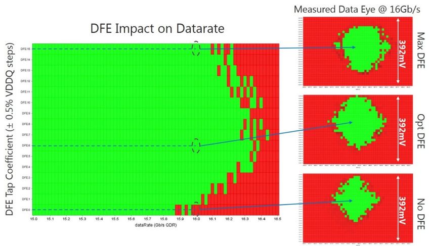
he worked as senior signal Integrity engineer in the area of wireless network system,
mobile chip & package, and mobile product at Samsung Electronics (Suwon, Korea).
Jörg Weller (M’07) was born in Munich, Germany in 1968. He received a diploma in
electrical engineering (M.S.E.E.) from the Technical University of Munich in 1994. He
joined Siemens AG in 1994, where he was responsible for the design and layout of a 4
M-bit DRAM, continuing with production wafer testing for RDRAMs in 1998. In 2001,
he started design analysis for graphics DRAMs with Infineon AG. Following the spin-off
of Qimonda AG in 2006, he continued design analysis work on GDDR3 and GDDR5
interfaces. In 2009, he joined Elpida Memory Europe and was involved in graphic
DRAM development. With the transition to Micron Technology, Inc. in 2012 he
continued to work on GDDR5, GDDR5x and GDDR6 graphic DRAM.

                                                                6
©2018 Micron Technology, Inc. All rights reserved. Information, products, and/or specifications are subject to change without
notice. All information is provided on an “AS IS” basis without warranties of any kind. Drawings may not be to scale. Micron, the
Micron logo, and all other Micron trademarks are the property of Micron Technology, Inc. All other trademarks are the property of
their respective owners. Rev. A, 01/18 CCM004‐676576390‐10965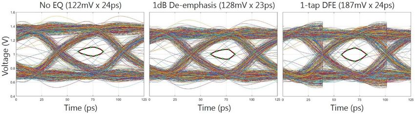
Introduction
GDDR5 has been an enabler of high performance applications for nearly 10 years. While
the first devices were introduced at a data rate of 6 Gb/s/pin [1], today, cards reaching 8
Gb/s/pin are readily available in the marketplace. Yet, even the fastest GDDR5 claimed is
only running at 9 Gb/s/pin [2]; barely exceeding the speed of parts already commercially
available. Thus, as successful as GDDR5 has been, this apparent slow-down in
bandwidth scaling needed to be addressed. To preempt the inevitable gap between market
bandwidth demands and available memory component performance, the industry has
pursued two parallel paths.
One approach has been to develop a completely new memory architecture, coincidently
named High Bandwidth Memory (HBM) [3]. With the understanding that memory
interface performance is limited primarily by the slower DRAM transistor process, as
well as the chip-to-chip interconnect, HBM chose to completely redefine the problem by
adopting an extremely wide (many wires) interface, thus allowing the DRAM
input/output (I/O) circuitry to operate well within the DRAM process capabilities. That
redefinition, however, requires a substantial enhancement in the supporting technologies;
namely the reliance on Silicon Interposer and Through-Silicon-Via (TSV) technologies to
couple the GPU/ASIC with the DRAM.
HBM, as it has been defined, thus consists of a TSV-interconnected stack of DRAMs
resting on a logic buffer die, which communicates with the GPU/ASIC across a fine-
pitched Si interposer-based channel at relatively low per-pin data rates. While the HBM
architecture offers many advantages, its complexity, in terms of testability, stability,
durability and overall cost have limited its adoption to only the highest-tier applications.
In parallel with the development of HBM, the more evolutionary path of the GDDR
family of DRAMs has continued to scale in performance, offering a more cost-effective
and flexible alternative. Without redefining the system, GDDR5X directly addressed the
key bandwidth limiters through internal data path and clocking enhancements [4], thus
providing for less risky adoption in more cost-sensitive applications (e.g., gaming, etc.,).
GDDR5X is currently found in the marketplace reaching per-pin data rates of up to 11.4
Gb/s [5].
Even as GDDR5X continues to make incremental improvements, the next natural step on
the GDDR path was to develop a GDDR6 standard capable of supporting per-pin data
rates doubling GDDR5. Presently the official GDDR6 JEDEC standard covers a range
from 12Gb/s – 14Gb/s, but in this paper, we will demonstrate GDDR6 scalability to at
least 16Gb/s/pin. The remainder of the paper is divided into three primary sections:
silicon changes (e.g., circuit and architecture) and channel enhancements required to
support scaling the single-ended GDDR interface all the way to 16Gb/s, along with
performance measurements of Micron Technology, Inc.’s first 8Gb, 16Gb/s/pin GDDR6
offering.

                                                                7
©2018 Micron Technology, Inc. All rights reserved. Information, products, and/or specifications are subject to change without
notice. All information is provided on an “AS IS” basis without warranties of any kind. Drawings may not be to scale. Micron, the
Micron logo, and all other Micron trademarks are the property of Micron Technology, Inc. All other trademarks are the property of
their respective owners. Rev. A, 01/18 CCM004‐676576390‐10965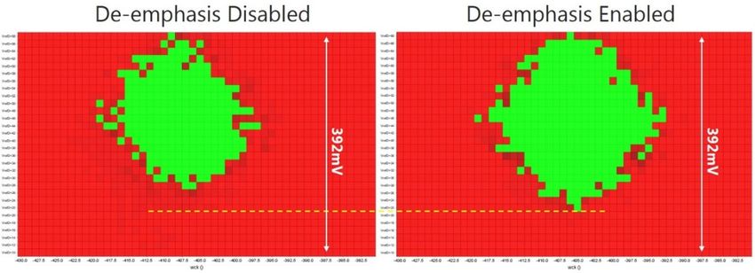
Figure 1: Die photo of Micron Technology, Inc.’s first 8Gb, 16Gb/s-capable
GDDR6 offering
Silicon Changes
An image of Micron Technology, Inc.’s first GDDR6 die is shown in Fig. 1. While
circuit and architectural changes were needed to achieve the new bandwidth target, a
primary goal of the GDDR6 component definition was to stay close to the evolutionary
path, and thus take advantage of the advanced GDDR5 and GDDR5X infrastructure,
including established packaging, handling and testing methods. As a result, external
features like the general command protocol have been held over from the previous
standards.
The most prominent new feature, in terms of system application, has been the added
support for dual-channel (2 x16) operation. Another change, visible to the system, is
support for stronger on-die termination and output driver pull-up strength of 48. While
the output driver remains somewhat asymmetric (60/40 or 48/40), this support for
48 improves signal symmetry, while providing a better match to the typical
characteristic impedance of the package + printed circuit board (PCB) channel for
enhanced signal integrity.
Aside from these changes, and some specification extensions related to Phase Locked
Loop (PLL) operation and clocking flexibility, GDDR6 speeds are enabled through the
accumulation of several incremental improvements over the GDDR generations. Data
Bus Inversion (DBI) was introduced as early as GDDR4, and has continued to prove
effective at mitigating simultaneous switching output (SSO) noise while lowering
signaling power [6]. Decision Feedback Equalization (DFE) for channel impairment
compensation, PLL for jitter filtering, regulated voltage supplies to minimize Power
8
©2018 Micron Technology, Inc. All rights reserved. Information, products, and/or specifications are subject to change without
notice. All information is provided on an “AS IS” basis without warranties of any kind. Drawings may not be to scale. Micron, the
Micron logo, and all other Micron trademarks are the property of Micron Technology, Inc. All other trademarks are the property of
their respective owners. Rev. A, 01/18 CCM004‐676576390‐10965
Supply Induced Jitter (PSIJ) in the high-speed Write Clock (WCK) distribution were all
included in early GDDR5 designs [1]. Output driver boosting (similar to pre-emphasis)
was incorporated into GDDR5 to open the data eye as speeds continued to push, while at
the same time, innovative internal modes of operation, like Frequency Controlled
Switching (FCS) of charge pumps, used to set the varied voltage levels throughout the
DRAM, proved helpful in reducing internal supply variation for greater stability along
the data path [7]. Duty cycle correction and input clock equalization, along with
inductive-capacitive (LC) resonant clock tree termination and a more prevalent use of
current-mode-logic (CML) circuit design enabled yet higher speeds through reducing
jitter in the DRAM clock distribution [2].
To overcome limitations in DRAM array timing, GDDR5X doubled the data prefetch,
increasing the number of bits presented to the output driver with each data access. To
double the datarate out of the DRAM without increasing the memory system clock
frequency, GDDR5X supports both Double Data Rate (DDR) and Quad Data Rate
(QDR) modes of operation. A PLL on the DRAM provides a degree of jitter filtering, and
at the same time may be used as a WCK frequency multiplier in QDR mode, though the
GDDR6 JEDEC specification provides flexibility in PLL usage, supporting high-speed
operation without the PLL. To improve signal integrity when reading data from the
memory, tunable de-emphasis was incorporated into the output driver structure; a non-
trivial design due to the inherent asymmetry in the unbalanced pull-up/pull-down drive
strength definition. Further, to guarantee a more robust interface, increasingly complex
and accurate training and calibration of the interface timing and voltage margins has
become essential [8], and, as needed, GDDR5 and beyond support per-pin de-skew of the
data bus. Finally, to ensure that errors are not introduced during chip-to-chip
communication, the results of Cyclic Redundancy Check (CRC) calculations are
transmitted from DRAM to the GPU/ASIC over an Error Detect Code (EDC) pin at half
of the data rate [4,7]. Nearly all of these incremental advances developed or adopted
throughout the history of GDDR find their place within the GDDR6 architecture, and in a
later section of this paper corresponding benefits will be quantified through
characterization of Micron Technology, Inc.’s GDDR6 silicon.

Channel Enhancements
While the chip-to-chip interconnect consists of several key components, many of which
are the responsibility of the system architect, one key channel component which is
defined within the JEDEC standard is the ball assignment for the ball grid array (BGA) of
the DRAM package. Not only does the ball assignment influence signal integrity within
the DRAM package, but it can either facilitate or hinder the routing of the main PCB
channel. This is because the relative proximity of signals in the ball grid extends into the
PCB through the vertical via transitions to the planar routing layers, which could be 100s
of microns deep within the PCB substrate. The ball grid often represents a compromise
between the needed signal integrity of the channel, the spatial requirements of the die
physical layer (PHY), the greater die architecture and cost. The ball grid should limit
                                                                9
©2018 Micron Technology, Inc. All rights reserved. Information, products, and/or specifications are subject to change without
notice. All information is provided on an “AS IS” basis without warranties of any kind. Drawings may not be to scale. Micron, the
Micron logo, and all other Micron trademarks are the property of Micron Technology, Inc. All other trademarks are the property of
their respective owners. Rev. A, 01/18 CCM004‐676576390‐10965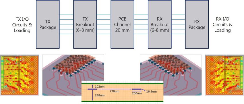
unwanted signal coupling (crosstalk) in the vertical interconnect, while promoting clean
routing of signals, including sufficient and consistent signal return paths to their optimal
locations at the silicon interface.

 Figure 2: Comparison of the JEDEC-specified BGA ball assignments for GDDR5X and
                   GDDR6 (upper-left quadrant, single-byte only).

Fig. 2 compares the upper-left quadrant of the JEDEC-specified GDDR5X and GDDR6
package ball assignments; each of the four quadrants supports a single byte of data lines.
While not shown in this format, the transition from GDDR5X to GDDR6 included a
slight increase in ball pitch from 0.65mm to 0.75mm. On the other hand, as shown, the
newly-defined GDDR6 ballout distributes the high-speed data signal balls over a larger
area within the grid by extending into the fourth column from the center of the package
(column 2), leading to several advantages. For example, VSS balls are more equally
distributed across the ball matrix resulting in better signal returns. Coupling between data
lines and the even more critical WCK lines is reduced, as well as coupling between data
and EDC pins. The proximity of uni-directional (WCK, EDC, etc.) and bi-directional
(DQ, DBI, etc.) signals in the package produces distinct coupling conditions during
DRAM Read and Write operations, and warrants careful analysis.
A qualitative evaluation of the worst-case data ball positions in the GDDR5X and
GDDR6 definitions projects that the DQ3 signal in the GDDR5X case will experience far
end crosstalk (FEXT) from DQ0, DQ1, DQ2 and WCK, with even more detrimental near
end crosstalk (NEXT) from the EDC signal. (NEXT is expected to be a greater concern,
as much of the FEXT will be mitigated through stripline routing of the high-speed
signals.) In the GDDR6 case, the DQ2 signal experiences FEXT from DQ0, DQ1 and
DQ3 and NEXT from EDC. Thus, the high-speed clocks have been spatially separated
from the single-ended data lines. Additionally, at least one aggressor has been removed
                                                               10
©2018 Micron Technology, Inc. All rights reserved. Information, products, and/or specifications are subject to change without
notice. All information is provided on an “AS IS” basis without warranties of any kind. Drawings may not be to scale. Micron, the
Micron logo, and all other Micron trademarks are the property of Micron Technology, Inc. All other trademarks are the property of
their respective owners. Rev. A, 01/18 CCM004‐676576390‐10965
from proximity to the EDC ball, which further increases the robustness of the interface.
Of course, this qualitative discussion does not account for the pin assignments at the far
(GPU) end of the channel, but the GDDR6 DRAM package ballout at least promotes
cleaner channel routing between chips.
Figure 3: Comparison of crosstalk in GDDR5X and GDDR6 DRAM packages.
Fig. 3 adds some data to this qualitative discussion of coupling, by presenting the sum of
a crosstalk within the DRAM package onto the worst-case DQ lines (left), DQ3 for
GDDR5X and DQ2 for GDDR6, along with the sum of all crosstalk onto the EDC lines
(right). A DRAM Write operation is assumed for both cases, and thus far-end coupling
from all signals onto the DQ of interest, with the exception of the EDC, is summed and
then combined with the corresponding near-end coupling from the EDC line in the left
plot. In the right plot, near-end coupling from all signals onto the EDC line is
accumulated.
While the package models were both extracted out to 40GHz, the GDDR5X extraction
accounted for half of the physical package, while the GDDR6 extraction only accounted
for a quadrant of the package, which may help to explain the apparent differences in
“smoothness” of the response curves. It is clear, however, from the left side of Fig. 3, that
the accumulated coupling onto the worst-case DQ is improved in the GDDR6 package,
consistent with our intuition-based comparison of the two ball-outs. The improvement in
the EDC response, on the right, may not be as clear, but poses less of a problem as the
specification allows for the EDC signal to toggle at half-rate.
As a developer of memory technologies, Micron Technology, Inc. does not often delve
into the world of system architecture and design. Yet, as all high-speed interface
designers know, it is difficult to produce an optimized composite channel when
developing the distinct component packages and main substrate connectivity in isolation.
Thus, to facilitate better DRAM packaging and I/O characteristics, Micron Technology,
Inc. purchased recent “off-the-shelf” high-speed graphics cards to study the typical
DRAM to GPU interconnect as a point of reference for channel optimization studies (see
11
©2018 Micron Technology, Inc. All rights reserved. Information, products, and/or specifications are subject to change without
notice. All information is provided on an “AS IS” basis without warranties of any kind. Drawings may not be to scale. Micron, the
Micron logo, and all other Micron trademarks are the property of Micron Technology, Inc. All other trademarks are the property of
their respective owners. Rev. A, 01/18 CCM004‐676576390‐10965Fig. 4). Such an approach has greatly increased our modeling confidence, in that our
assumptions (channel length, pitch, stack-up, etc.) are justified through commercially
available technologies.
Figure 4: Exemplary GPU-to-DRAM channel from an “off-the-shelf” graphics card.
Figure 5: End-to-end channel model producing all simulation results throughout this
paper.
That said, none of the simulation results shared in this paper correspond directly to an
analyzed graphics card channel. Rather, we have chosen to share results based on
simulations couched in distinct, yet reasonable assumptions. Our end-to-end channel
12
©2018 Micron Technology, Inc. All rights reserved. Information, products, and/or specifications are subject to change without
notice. All information is provided on an “AS IS” basis without warranties of any kind. Drawings may not be to scale. Micron, the
Micron logo, and all other Micron trademarks are the property of Micron Technology, Inc. All other trademarks are the property of
their respective owners. Rev. A, 01/18 CCM004‐676576390‐10965model is symmetric, assuming the via transitions below the DRAM package, as well as
the DRAM package routing / construction, at both ends of the link, as shown in Fig. 5.
As indicated in the figure, the channel is broken into segments to allow for more accurate
3D modeling of the vertical interconnect and package, while the main PCB route is
represented by 2D models for flexibility in studying the impact of channel length, data
line width, routing pitch, stack-up, etc. Both ends of the channel are terminated,
depending on the direction of the signaling operation, through 48Ω or 60Ω to a 1.35V
VDDQ supply. The parasitic capacitive loading at the die pad is assumed to be 0.5pF at
each end of the channel. While countless transistor-level simulations have been
completed for both the output and input paths of the DRAM, all simulation results shown
in this paper are based on linear driver modeling to enable rapid, peak distortion analysis
(PDA) of worst case pattern conditions [9]. We acknowledge that the unmatched pull-
up/pull-down characteristics of the driver cannot be perfectly captured through linear
modeling, but we remain confident, based on internal modeling correlation, that this
assumption does not significantly alter the results of the paper.
As a goal of this paper is to demonstrate bandwidth scalability in GDDR6, Fig. 6 presents
the worst-case data eye openings at 14Gb/s and 16Gb/s for the baseline model. It is
important to note that the platforms, on which the exemplary channel models were based,
were not designed to support 16Gb/s. Thus, the cases shown in Fig. 6 potentially push
beyond the boundaries of expected performance. Nevertheless, it is observed that with the
available DFE functionality incorporated into GDDR6, this channel delivers an open eye
at 14Gb/s. At 16Gb/s, however, the received data eye is completely closed, even after
equalization.
Figure 6: Baseline channel simulation employing available single-tap DFE, but without
any other channel enhancements.
13
©2018 Micron Technology, Inc. All rights reserved. Information, products, and/or specifications are subject to change without
notice. All information is provided on an “AS IS” basis without warranties of any kind. Drawings may not be to scale. Micron, the
Micron logo, and all other Micron trademarks are the property of Micron Technology, Inc. All other trademarks are the property of
their respective owners. Rev. A, 01/18 CCM004‐676576390‐10965What steps then may be taken to enable 16Gb/s signaling over this basic channel
structure (e.g., materials, distance, routing cross-section, etc.)? One option, not
incorporated into the model that produced the eyes in Fig 6, is the well-known back
drilling of vias to mitigate impedance discontinuities and crosstalk in the vertical
interconnects below the component packaging. In the simulation world, it is
straightforward to evaluate what impact a process like back drilling would have on
overall performance.
Much can be learned from the channel pulse response, as presented in Fig. 7. First, a few
details. For simplicity, all PDA-based calculations are done on a sample basis (e.g., x
samples per unit interval (UI)) rather than on absolute time. While the pulse responses
shown are labelled as “volts” and “sample”, final eye measurements are output as
absolute voltage and time. All cursors highlighted in red are separated by 1 UI (62.5ps)
and are shifted such that the main cursor aligns with the center of the resulting data eye.
While only 13 post cursors are shown, several additional cursors are captured and
included in all eye closure calculations. The number of cursors must be chosen so as not
to ignore perturbations later in the pulse tail. This is particularly true for a high-speed
graphics channel, which, being relatively loss-less, may support lingering reflections
resulting from imperfect channel termination, as well as other discontinuities.
Figure 7: Pulse response comparison of the channel without and with via back drilling.
Fig. 7 compares the 16Gb/s pulse responses for a common data line with and without
back drilling. Qualitatively it is observed that back drilling positively impacts the channel
response in a variety of ways. First it increases the main cursor value (amplitude), while
reducing the first three post cursors significantly. Further it greatly reduces the magnitude
of the signal reflection dispersed over post cursors 8-13. Based on the superposition of
the pre-cursor and first 13 post-cursors alone, PDA projects vertical eye openings of
428.16mV and 269.65mV with and without back drilling, respectively. While one might
14
©2018 Micron Technology, Inc. All rights reserved. Information, products, and/or specifications are subject to change without
notice. All information is provided on an “AS IS” basis without warranties of any kind. Drawings may not be to scale. Micron, the
Micron logo, and all other Micron trademarks are the property of Micron Technology, Inc. All other trademarks are the property of
their respective owners. Rev. A, 01/18 CCM004‐676576390‐10965expect 269.65mV to provide sufficient margin, in the presence of crosstalk the closed
data eye shown on the right side of Fig. 5 is not necessarily surprising, even with DFE.
To validate this last statement regarding the degree of crosstalk observed across the
channel, Fig. 8 compares the un-equalized back-drilled case, with and without aggressors
(e.g., all remaining DQ lines in the Byte, along with the EDC and DBI signals). Based on
this simulation, about 238mV of crosstalk is expected in the cleaner (e.g., back-drilled) of
the two channel environments. More crosstalk would be expected in the absence of back
drilling. Thus, as a goal of this paper is to demonstrate a practical path to 16Gb/s, all
remaining simulations assume back drilling of vias in the PCB as a foundation for
additional enabling steps, including equalization.
Figure 8: Simulated data eye openings at 16Gb/s – ISI only (left) and with additive
crosstalk from the remaining high-speed data lines, EDC and DBI signals (right).
Based on a further review of the raw pulse response from the right side of Fig. 7, a
practical, power-efficient equalizer solution might only need to address the 1st post
cursor. The GDDR6 I/O incorporates both tunable single-tap de-emphasis into the output
driver and tunable single-tap DFE within the input path, both designed to operate on the
1st post cursor. Fig. 9 compares the relative effectiveness of the available de-emphasis
and DFE. As shown, the de-emphasis improves the eye height by 6mV, while degrading
the eye width by 1ps. The DFE, on the other hand, improves the eye height by 65mV
without degrading the eye width. It is important to note that the results shown are
channel-specific and are insufficient to make a universal assessment of the relative value
of either equalization method, though some qualitative observations can be made when
comparing the corresponding pulse responses, as demonstrated by Fig. 10.
15
©2018 Micron Technology, Inc. All rights reserved. Information, products, and/or specifications are subject to change without
notice. All information is provided on an “AS IS” basis without warranties of any kind. Drawings may not be to scale. Micron, the
Micron logo, and all other Micron trademarks are the property of Micron Technology, Inc. All other trademarks are the property of
their respective owners. Rev. A, 01/18 CCM004‐676576390‐10965Figure 9: Simulated data eye openings at 16Gb/s – No equalization (left), single-tap de-
emphasis (center) and single-tap DFE (right).
As highlighted in Fig. 10, de-emphasis-based equalization (green and blue curves)
reduces the overall amplitude of the signal while reducing the 1st post cursor. As a result,
the optimal amount of de-emphasis corresponds to a balance between signal amplitude
and ISI cancellation. For the channel under consideration, 3dB of de-emphasis (blue
curve) nearly reduces the 1st post cursor to zero, yet, as will be shown, a larger eye
opening is possible with only 1dB of de-emphasis (green curve). This is because 3dB of
de-emphasis does not leave enough of the main cursor to provide a net increase in eye
opening, while 1dB of de-emphasis, on the other hand, results in a net positive of 6mV.
Intuitively, because the DFE zeros out the 1st post cursor without reducing the signal
amplitude, one would expect a better overall result, which is clearly demonstrated in Fig.
9. One other nuance captured in Fig. 10 is that de-emphasis, while primarily addressing
the 1st post cursor, may impact additional post cursors for better or worse. As shown in
this particular case, the 2nd post cursor is degraded slightly by de-emphasis, while this
behavior does not occur with DFE. However, this same fact that de-emphasis may affect
more than just the tap in question could produce much better results under different
channel conditions.
16
©2018 Micron Technology, Inc. All rights reserved. Information, products, and/or specifications are subject to change without
notice. All information is provided on an “AS IS” basis without warranties of any kind. Drawings may not be to scale. Micron, the
Micron logo, and all other Micron trademarks are the property of Micron Technology, Inc. All other trademarks are the property of
their respective owners. Rev. A, 01/18 CCM004‐676576390‐10965Figure 10: Overlay of channel pulse responses comparing various equalization methods.
Fig. 11 presents two additional equalization conditions. As shown on the left, when
combining the “best” amount of de-emphasis, namely 1dB, with a corresponding
optimized tap of DFE (to cancel the remaining 1st post cursor ISI), the resulting eye is
smaller than that achieved by applying DFE alone (see right side of Fig. 9). This is
because the de-emphasis unnecessarily reduces the signal amplitude and the DFE offers
no gain to compensate for that reduction. The eye diagram on the right of Fig. 11,
corresponding to 3dB of de-emphasis, is also interesting. Recalling from the pulse
responses of Fig. 10 that even though 3dB of de-emphasis would almost perfectly zero
out the 1st post cursor, the resulting eye height remains identical to the un-equalized case
(while the timing degrades by 3ps). Comparison of this eye with the original un-equalized
eye in Fig. 9 reveals that the ISI is, indeed, reduced by the de-emphasis, but the overall
signal amplitude is reduced by a similar amount (at least when all of the crosstalk and
reflections are accounted for).
17
©2018 Micron Technology, Inc. All rights reserved. Information, products, and/or specifications are subject to change without
notice. All information is provided on an “AS IS” basis without warranties of any kind. Drawings may not be to scale. Micron, the
Micron logo, and all other Micron trademarks are the property of Micron Technology, Inc. All other trademarks are the property of
their respective owners. Rev. A, 01/18 CCM004‐676576390‐10965Figure 11: Simulated data eye openings at 16Gb/s – Combined de-emphasis and DFE
(left) and stronger (3dB) de-emphasis (right).
Two final observations regarding equalization. It is worth noting that none of the
equalization methods described herein improve eye width. Thus, every effort should be
made to minimize crosstalk across these high-speed parallel interconnects. It is also
important to understand that while additional equalization methods could be employed in
this application, such are not explicitly called for by the JEDEC GDDR6 specification,
and therefore are not evaluated here. Nevertheless, 1-tap of DFE, coupled with the back-
drilling of PCB vias, appears sufficient to support 16Gb/s signaling.
GDDR6 Performance Measurements
As it is generally helpful to increase confidence through complimenting simulation with
measured results, ATE-based characterization of Micron Technology, Inc.’s first GDDR6
offering is shared, beginning with Fig. 12, which compares the measured link margin at
16Gb/s and 16.5Gb/s, based on shmooing the DRAM and tester reference voltages along
with the phase of the data relative to the data clock and strobe. Green and Red points
distinguish between error-free operation, and the detection of errors, respectively. As
shown, GDDR6’s support for the stronger 48Ω termination is expected to improve
signaling margins, especially at higher speeds.
18
©2018 Micron Technology, Inc. All rights reserved. Information, products, and/or specifications are subject to change without
notice. All information is provided on an “AS IS” basis without warranties of any kind. Drawings may not be to scale. Micron, the
Micron logo, and all other Micron trademarks are the property of Micron Technology, Inc. All other trademarks are the property of
their respective owners. Rev. A, 01/18 CCM004‐676576390‐10965Figure 12: Measured link margin shmoos at 16Gb/s/pin and 16.5 Gb/s/pin for 60Ω and
48Ω line termination.
Fig. 13 presents the impact of DFE from two perspectives. First, the maximum
achievable data rate (x-axis), as determined by an agreed-upon degree of eye opening
(height and width), is plotted against an increasing amount of DFE compensation (y-
axis). There are at least two key take-aways. First, the observation that, in spite of the
relatively clean tester environment, there is a clear benefit to be gained in optimizing the
DFE coefficient selection, above and below which the maximum achievable data rate is
degraded. And second, 16Gb/s is nearly achievable without DFE, and thus the
equalization adds margin and reliability to the interface.
19
©2018 Micron Technology, Inc. All rights reserved. Information, products, and/or specifications are subject to change without
notice. All information is provided on an “AS IS” basis without warranties of any kind. Drawings may not be to scale. Micron, the
Micron logo, and all other Micron trademarks are the property of Micron Technology, Inc. All other trademarks are the property of
their respective owners. Rev. A, 01/18 CCM004‐676576390‐10965Figure 13: Measured achievable data rate shmoo (left) and corresponding link margin
shmoos for three DFE settings: no equalization (bottom-right), optimal DFE (center-
right) and maximum DFE (top-right).
For a deeper comparison, the right side of the figure presents three measured link margin
shmoos corresponding to no equalization, optimal DFE setting, and maximum (not
optimal) DFE. Interestingly, the non-optimized, maximum DFE setting does not degrade
the results substantially, but the optimal setting clearly represents the best solution, in
terms of symmetry and overall eye height. Fig. 14 presents the impact of enabling de-
emphasis. Based on these results, de-emphasis appears to provide substantial benefit over
the ATE channel.
Figure 14: Measured link margin shmoos at 16Gb/s without and with single-tap de-
emphasis enabled.
20
©2018 Micron Technology, Inc. All rights reserved. Information, products, and/or specifications are subject to change without
notice. All information is provided on an “AS IS” basis without warranties of any kind. Drawings may not be to scale. Micron, the
Micron logo, and all other Micron trademarks are the property of Micron Technology, Inc. All other trademarks are the property of
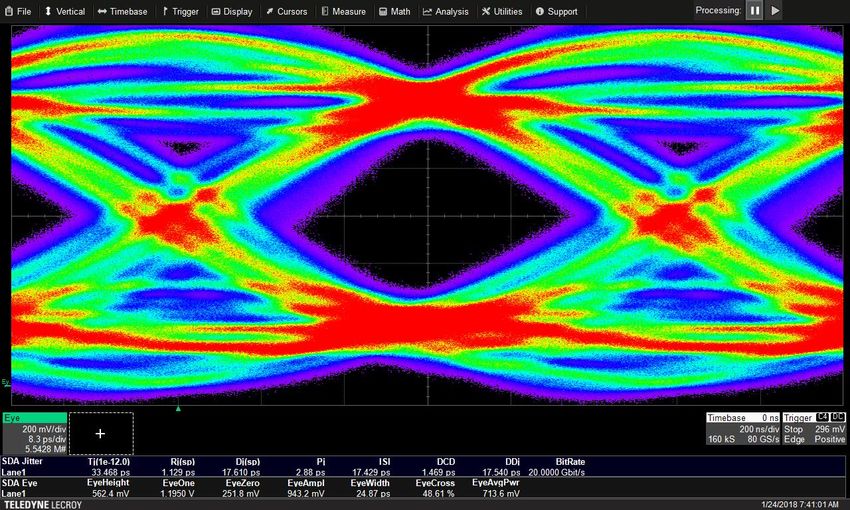
their respective owners. Rev. A, 01/18 CCM004‐676576390‐10965Figure 15: Measured 20Gb/s data eye based on a PRBS6 pattern
While the preceding results demonstrate full DRAM functionality up to as high as
16.5Gb/s, it is possible for the overall performance of an architecture to be capped by
timing limitations in the memory array itself. To determine if this GDDR6 interface could
extend beyond the 16.5Gb/s range, the device was placed into a mode of operation which
exercises only the I/O while bypassing the memory array. The oscilloscope measurement
presented in Fig.15 confirms that when bypassing the memory array, and with a small,
but helpful, boost in I/O supply voltage, it is possible to push Micron Technology, Inc.’s
GDDR6 I/O as high as 20Gb/s.
Summary
As compute systems continue to advance, their efficacy often depends on the
accessibility of memory. While some high-tier applications can absorb the high cost and
complexity of HBM, the performance of GDDR DRAM continues to scale, providing a
more flexible, low-risk, cost-effective alternative. Through reviewing the current state of
GDDR5X and ATE-based measurements of Micron Technology, Inc.’s first GDDR6
offering, along with known circuit and channel enhancements (namely an improved
DRAM package ball out definition with looser pitch and via back drilling within the
PCB), we are confident in claiming that GDDR6 data rates will extend beyond the
14Gb/s/pin target defined by JEDEC all the way to 16Gb/s/pin. As a result, GDDR6
looks to be an attractive compliment for generations to come.
21
©2018 Micron Technology, Inc. All rights reserved. Information, products, and/or specifications are subject to change without
notice. All information is provided on an “AS IS” basis without warranties of any kind. Drawings may not be to scale. Micron, the
Micron logo, and all other Micron trademarks are the property of Micron Technology, Inc. All other trademarks are the property of
their respective owners. Rev. A, 01/18 CCM004‐676576390‐10965References:
[1] S. J. Bae et al., "A 60nm 6Gb/s/pin GDDR5 Graphics DRAM with Multifaceted
Clocking and ISI/SSN-Reduction Techniques," ISSCC-2008, pp. 278-613.
[2] H. Y. Joo et al., "A 20nm 9Gb/s/pin 8Gb GDDR5 DRAM with an NBTI monitor,
jitter reduction techniques and improved power distribution," ISSCC-2016, pp. 314-315.
[3] D. U. Lee et al., "1.2V 8Gb 8-channel 128GB/s high-bandwidth memory (HBM)
stacked DRAM with effective microbump I/O test methods using 29nm process and
TSV," ISSCC-2014, pp. 432-433.
[4] M. Brox et al., “An 8Gb 12Gb/s/pin GDDR5X DRAM for Cost-Effective High-
Performance Applications”, ISSCC-2017, pp. 388-389.
[5] NVIDIA TITAN Xp – Design & Visualization, https://www.nvidia.com/en-us/design-
visualization/products/titan-xp/, Accessed November 3, 2017
[6] T. M. Hollis, “Data Bus Inversion in High-Speed Memory Applications,” IEEE
Transactions on Circuits and Systems II: Express Briefs, vol. 56, no. 4, April 2009.
[7] R. Kho et al., "A 75 nm 7 Gb/s/pin 1 Gb GDDR5 Graphics Memory Device with
Bandwidth Improvement Techniques," in IEEE Journal of Solid-State Circuits, pp. 120-
133, Jan. 2010.
[8] A. Shiloy, “GDDR5X Standard Finalized by JEDEC: New Graphics Memory up to
14 Gbps,” January 22, 2016., https://www.anandtech.com/show/9883/gddr5x-standard-
jedec-new-gpu-memory-14-gbps, Accessed November 3, 2017.
[9] B. K. Casper, M. Haycock and R. Mooney, "An accurate and efficient analysis
method for multi-Gb/s chip-to-chip signaling schemes," 2002 Symposium on VLSI
Circuits. Digest of Technical Papers (Cat. No.02CH37302), Honolulu, HI, USA, 2002,
pp. 54-57.
22
©2018 Micron Technology, Inc. All rights reserved. Information, products, and/or specifications are subject to change without
notice. All information is provided on an “AS IS” basis without warranties of any kind. Drawings may not be to scale. Micron, the
Micron logo, and all other Micron trademarks are the property of Micron Technology, Inc. All other trademarks are the property of
their respective owners. Rev. A, 01/18 CCM004‐676576390‐10965You can also read