Development of a long pulsed RF test stand and its applications for performance studies of 1 MW CW klystron
←
→
Page content transcription
If your browser does not render page correctly, please read the page content below
Sådhanå (2020)45:36                                                                                                               Ó Indian Academy of Sciences
https://doi.org/10.1007/s12046-020-1281-z   Sadhana(0123456789().,-volV)FT
                                                                        3](0123456789().,-volV)

Development of a long pulsed RF test stand and its applications
for performance studies of 1 MW CW klystron
           PURUSHOTTAM SHRIVASTAVA, T REGHU* , J MULCHANDANI, V MANDLOI,
           P MOHANIA, A MAHAWAR, HARGOVIND SINGH and VIKAS RAJPUT

           Pulsed High Power Microwave Division, Raja Ramanna Centre for Advanced Technology (RRCAT),
           Indore 452013, India
           e-mail: traghu@rrcat.gov.in

           MS received 22 February 2019; revised 23 December 2019; accepted 24 December 2019

           Abstract. Research and development activities of high power microwave sources for powering RF cavities of
           Indian Spallation Neutron Source and Accelerator Driven Subcritical Systems are underway at RRCAT. Front
           end accelerating structures such as Radio Frequency Quadrupoles and Drift Tube Linac demand pulsed RF
           power up to 1 MW. A 1 MW pulsed RF system based on TH 2089 klystron amplifier at 352.2 MHz with pulse
           width capability up to 1.5 ms has been developed and tested. A compact 100 kV, 20 A converter type modulator
           with pulse width capability up to 1.6 ms has been used to energize the klystron of RF test stand. The perfor-
           mance of the klystron in pulsed mode operation has been studied and presented. The variation in the RF output
           power was measured and it is within ±0.75%. The phase variation of RF output power within the pulse and the
           pulse to pulse is less than ±2.5°.

           Keywords.      Pulsed RF test stand; high power klystron; converter modulator; long pulsed modulator.

1. Introduction                                                                                   problem of the droop, pulse transformer needs to be
                                                                                                  carefully designed. In hard switched modulators there is no
High power klystron amplifiers are widely used for pow-                                           concern of the ripple and only the droop need to be man-
ering Radio Frequency (RF) cavities of high energy particle                                       aged by careful design of the pulse transformer and the
accelerators [1]. They are available in both continuous                                           bouncer circuit [7].
wave (CW) and pulsed mode operating conditions. High                                                 Another important concern with regard to the life of the
voltage pulsed sources are required for powering the kly-                                         klystron is the fault energy of the modulator in case of
stron amplifier and such sources are known as modulators.                                         internal arc in the klystron. Typically, 10 J is the allowable
Conventionally, line type and hard switched modulators                                            energy limit and beyond this limit, it can cause severe
based on tube switches are used for the generation of pulsed                                      damage to the klystron [8, 9]. Line type modulators are
high voltages [2, 3]. Line type modulators are normally                                           inherently current limited due to the presence of impedance
used for short and fixed output pulse width (typically less                                       of the PFN and leakage inductance of the pulse transformer
than 20 ls) applications. For the longer pulse width,                                             in series with the klystron. In the worst case, the maximum
modulator system would be very large as the width of pulse                                        current will be twice of the rated current. In the case of hard
is directly proportional to number of PFN stages [4]. Hard                                        switched modulators, entire energy stored in the input
switched modulators are used for both short and long pulse                                        storage capacitor gets dissipated in the klystron. To avoid
applications. The performance of klystron with line type                                          this situation, a suitable crowbar circuit is incorporated in
and hard switched modulators has been well studied as                                             parallel with the energy storage capacitor of the modulator
these topologies are in use for the past many decades [5].                                        [3]. In the event of an arc, the klystron current is sensed and
Other than rise and fall times which directly affect the                                          it generates a trigger to crowbar switch, thus diverting and
efficiency of RF system, the droop and the ripple in the                                          dissipating the energy stored in the storage capacitor in an
output pulse are other major concerns as they introduce                                           alternate circuit through the crowbar switch. The
phase delay in the RF output of klystron [6]. A well                                              advancement in the technology of semiconductor switches
designed line type modulator system with large number of                                          with high voltage, high current, high switching frequency
PFN stages will considerably reduce the ripple but for the                                        capabilities leads to the development of advanced solid
                                                                                                  state modulators [1, 10]. Solid state switches gradually have
*For correspondence                                                                               replaced thyratron switches of the conventional line type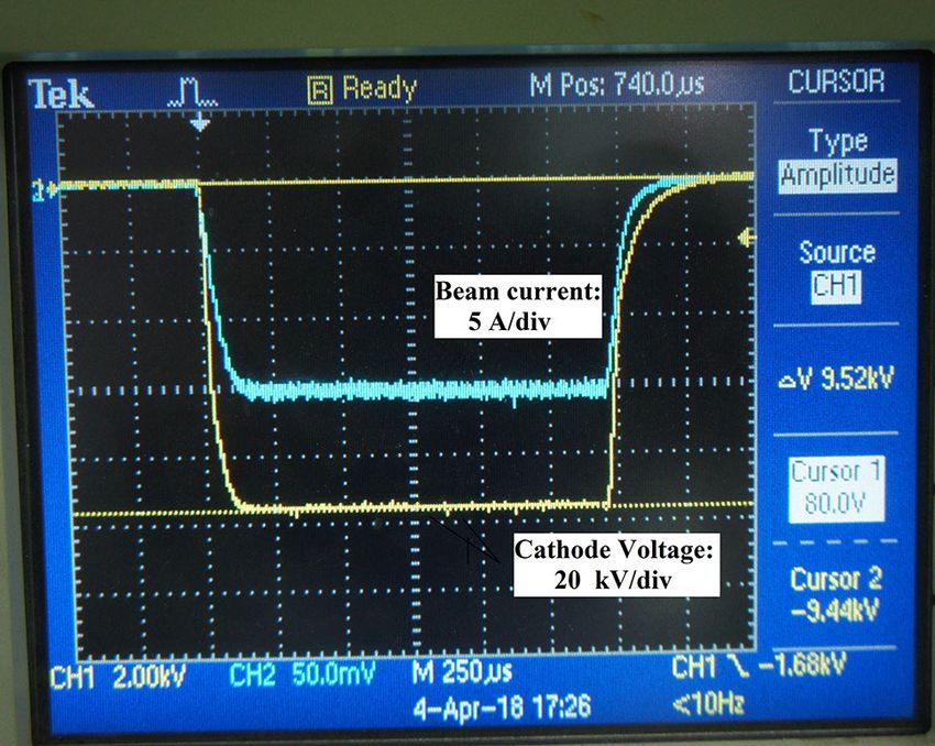
36 Page 2 of 7 Sådhanå (2020)45:36
modulators. Recently new type of modulators viz., the high voltage long pulses. The desired output pulse
converter and Marx type are gaining popularity for long width is achieved by gating the gate drives by the required
pulse (up to 5 ms pulse width) and high average power pulse width. The modulator system is modular and there are
applications. Among the two, converter type modulators are two identical modules and each generates -50 kV, thus
more popular for driving klystrons for the development of overall output is -100 kV. Each module consists of high
high energy particle accelerators for spallation neutron frequency switched inverters (fs = 20 kHz), high voltage
sources [11]. Additionally converter type modulators are high frequency transformer and fast six pulse rectifier. The
compact, inherently energy limited and there is no need of control circuits, droop correction circuits and low pass p-
any high voltage crowbar switch [12]. section filter are common to both the modules. The full
Pulsed High Power Microwave Division of Raja bridge inverter works on parallel loaded resonant (PLR) LC
Ramanna Centre for Advanced Technology, Indore, India, topology. PLR topology inherently offers higher gain of
has been pursuing research and development (R&D) on the output voltage depending on the overall quality factor
long pulsed klystron modulators [12–14]. Other than the (Q) of the topology. This is advantageous in lowering the
popular topologies for the generation of high voltage long turns-ratio of the transformer. The non-idealities of the
pulse, we have an R&D program on dc-dc converter based transformer are also effectively used as a part of the reso-
modulators also. In the past, design and development of a nant circuit.
33 kV, 20 A, 1.6 ms long pulse modulator has already been The high voltage and high frequency transformer has
reported for driving low voltage klystrons and inductive been developed using Fe based nanocrystalline core mate-
output tube (IOT) applications [12]. Very recently work on rial (VITROPREM 800 of Vacuumschmelze) [16]. The flux
the development of 100 kV, 20 A, 1.6 ms long pulse density is chosen as 0.6 T. Primary and secondary windings
modulator for driving 1 MW klystron has been reported are made using a litz wire. Since the secondary winding
[15]. Such modulators are relatively new and their effects needs high voltage insulation, a specially fabricated solid
on the performance of the continuous wave (CW) klystrons Teflon bobbin has been used. Fast recovery epitaxial diodes
are not well studied. In order to study the pulsed mode are used in the six pulse rectifier. Each arm is a series
performance of a klystron driven by long pulsed modulator combination of many diodes. A p-section low pass filter has
and to test various RF components of the accelerator sub- been used to filter out the 120 kHz ripple. All high voltage
systems, an RF test stand has been developed. In this paper, components are assembled in a stain less steel tank filled
we will describe the details of test stand and performance with transformer oil for insulation and cooling. The ‘phase
characteristics of the klystron amplifier in pulsed mode shift control’ in tandem with feed forward correction
operation. The operational parameters of the RF test stand scheme has been employed for droop correction of the
are given in table 1. output pulse. With this technique, a droop of less than ±1%
has been achieved. Finer details about the modulator are
given in the reference [15].
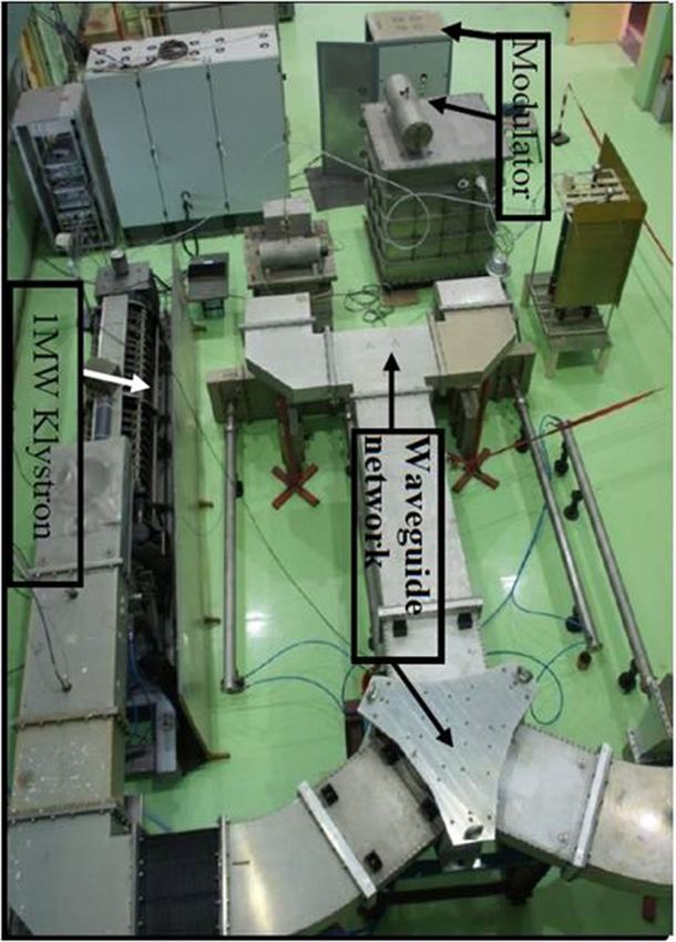
2. Pulsed RF test stand The klystron amplifier, TH 2809, (Thales Electron
Devices make) is a high power linear beam vacuum tube
The simplified block diagram of RF test stand is shown in device that amplifies RF signal [17]. It has 1.1 MW output
figure 1. It consists of a 2 MW (-100 kV, 20 A) pulsed power capability at nominal frequency of 352 MHz with
modulator, 1 MW klystron, WR 2300 waveguide trans- -1 dB bandwidth of 1 MHz. The tube has five integrated
mission system, RF measurement system, solid state power cavities, two integral electromagnets for focusing the beam
amplifier driver and water loads to dissipate the microwave within the klystron and a modulating anode to adapt
power. The pulsed modulator system is based on DC–DC specific operating conditions. When the electron beam
converter topology and employs IGBT switches which passes through the resonant cavities of klystron there is a
operate at lower supply voltage and higher switching fre- strong beam-RF interaction. While passing through the
quency. High frequency, high voltage transformers in cavities, the energy of the electron beam amplifies the input
conjunction with a series of fast recovery diodes generate signal applied to the first cavity. The catcher cavity at the
other end of the tube delivers the amplified output. The
electrons are finally captured by an anode cooled by low
Table 1. Operational parameters of RF test stand.
conductivity water (LCW).
RF output power (peak) 1 MW Solid state pulsed amplifier based on Laterally Diffused
Pulse width (max) 1.5 ms RF MOSFET (LDMOS) devices has been developed to
RF frequency (nom) 352.2 MHz energize input of the klystron. The amplifier consists of two
Droop ±0.75% stages, a driver and a high power stage, and operates in
Phase stability (in pulse) ±2.5° class AB mode. It has gain of *47 dB and generates
Phase stability (pulse to pulse) ±2.5°
pulsed power in excess of 200 W. A Rhode and Schwarz
Modulator output power 2 MW
make, precision signal generator, SMB 100 A, has been
PRR capability 1–30 Hz
used for driving the amplifier. The output of the solid state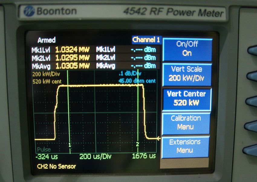
Sådhanå (2020)45:36                                                                    Page 3 of 7   36

                                      Figure 1. A simplified block diagram RF test stand.

amplifier is fed to the input port of the klystron. The output   common point of heater and cathode to avoid emission
RF power from klystron is coupled from its output ceramic        from back of the cathode surface. The Sputter Ion Pump
window and fed to a water (LCW) load through a WR2300            (SIP) of the klystron has been powered by Vacion make
waveguide network. An Advanced Ferrite Technology                5 kV, 50 mA power supply. The coils of focusing elec-
make three port circulator suitable for 352 MHz and high         tromagnets of the klystron have been powered by 250 V, 20
power operation has been used for isolation between the          A DC power supplies. The supply to the modulating anode
source and load and it has a -40 dB isolation. In the            of the klystron has been derived from same cathode pulsed
waveguide network, full height to half height tapered sec-       power supply using a resistive divider.
tion has been used to reduce the overall length of the net-         The modulating anode plays major role in the CW kly-
work and to couple E- plane half height magic tee. 1 MW          strons mainly for output power control or pulsed mode
pulsed RF power is finally dumped into four numbers of           operation. In this case the cathode voltage itself is in the
250 kW water loads. These four loads are connected at the        pulsed mode, therefore, for maximum output power the
output ports of magic tees. One more 250 kW load has been        modulating anode voltage is kept at 71% of the cathode
connected at the termination port of the circulator to absorb    voltage. A resistive divider has been used for the generation
the reflected power, if any. A higher order mode filter is       of modulating anode voltage and it is kept in an oil tank for
connected in the network to filter out the higher order          providing cooling and high voltage insulation. The klystron
modes generated at high power levels. Directional coupler        collector, body and RF output window are cooled by cir-
has been used at the klystron output to measure both the         culating LCW. The klystron body has been electrically
forward and the reflected powers. The forward and reflected      grounded by low impedance ground. The LCW flow circuit,
coupling factors are -50.1 dB and -44.8 dB, respectively.        vacuum status of klystron, cathode heater, and focussing
Boonton make pulsed power meter, model 4542, has been            coil power supplies are interlocked with the main modu-
used for measurement peak power and it has an RF fre-            lator to avoid any failure of the former systems. A relay
quency range of 10 kHz to 40 GHz and pulse power                 based, hardwired interlocking circuit has been used for this
measurement range of -50 to ?20 dBm.                             purpose. The aerial view of the experimental set-up is
   The cathode heater filament of klystron is powered by a       shown in figure 2.
30 V, 35 A DC power supply that is 120 kV isolated as the
cathode is floating during the high voltage pulse [18]. The
high voltage portion of the power supply is kept in trans-
former oil and the feedback signals of the output voltage        3. Results of performance studies and discussion
and the current are taken through fiber optic link for dis-
play. DC powering to klystron heater is preferred so that        Klystron is a nonlinear high power microwave amplifier
there is no AC magnetic field generated by AC heater             and the output power not only depends on cathode voltage
current near cathode area. Such AC magnetic field extends        and RF input power as in the conventional amplifiers but it
to the cathode surface and perturbs the beam trajectories        also depends on other parameters. The variation of output
causes variation in the beam current [17]. The negative          power with respect to cathode voltage has been studied and
terminal of heater power supply is connected to one of the       plotted in figure 3. The output RF power has a following
heater terminal and positive terminal is connected to            relation with cathode voltage,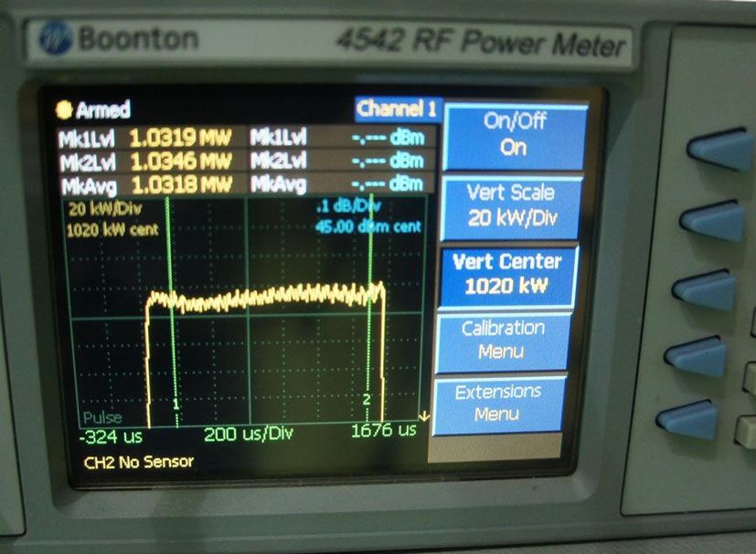
36 Page 4 of 7 Sådhanå (2020)45:36
function relationship between the output power and the
cathode voltage. Output power of 968 kW at 352.6 MHz
has been extracted from the klystron. The cathode voltage
beyond 96 kV is not tried due to chance of klystron arcing.
Figures 4 and 5 show the temporal shape of the cathode
voltage, beam current and RF power at maximum cathode
voltage of 96 kV. It is observed that the variation in the RF
power is within ±0.75% as shown in figure 6.
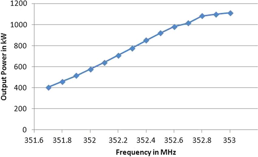
The variation in RF output power with respect to drive
frequency has been studied around the centre frequency of
352.21 MHz. The klystron has a -1 dB bandwidth of
1 MHz.
The drive frequency is varied from 351.7 MHz to
353 MHz keeping other inputs such as cathode voltage,
input RF power and currents of focusing magnets constant.
The output power increases as the drive frequency
approaches the centre frequency. An unusual behaviour has
been observed with increase in drive frequency beyond the
centre frequency the output power continues to increase as
opposed to the expected behaviour. This could possibly be
due to a different centre frequency than the specified one.
When output went beyond 1 MW, arcing was occasionally
observed in the LCW based loads, hence, no further
increase in frequency was tried. Figure 7 shows the varia-
tion in RF output power with respect to drive frequency.
During this experiment all other parameters were kept
constant.
Figure 2. Aerial view of RF test stand.
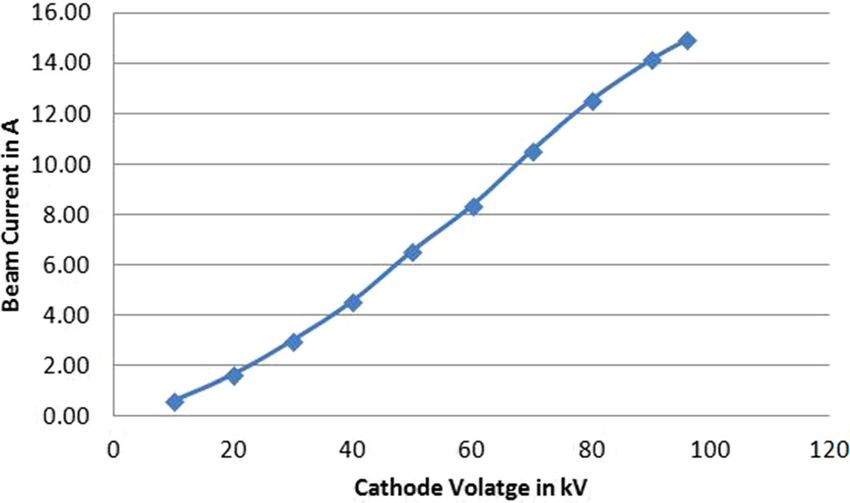
The klystron has a diode like characteristic and beam
current varies as three-and-a-half power of the voltage. The
relation between beam current and cathode voltage is
given by
3
Ib ¼ KV 2 ;
where Ib is the beam current, K is the perveance of the
klystron tube and V is the cathode voltage. Peak value of
Figure 3. RF output power versus cathode voltage.
5
P ¼ gPl 106 V 2 ;
where g is the efficiency, Pl is the microperveance and V is
the cathode voltage. Below -20 kV, the output power is
negligible and at lower voltages the output power increases
slowly due to low electron velocity [19]. At higher cathode Figure 4. Waveform of cathode voltage and beam current at
voltages the output power changes rapidly due to the power 96 kV.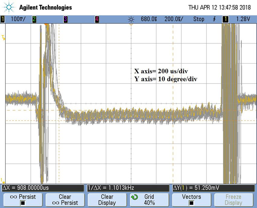
Sådhanå (2020)45:36                                                              Page 5 of 7     36

                                                                  Figure 8. Beam current versus cathode voltage.

   Figure 5. Temporal profile of the RF output of klystron.

Figure 6. Temporal profile of the RF output (expanded:
20 kW/div) of klystron.
                                                               Figure 9. RF output phase variation within the pulse.

     Figure 7. RF Output power versus drive frequency.

the beam current has been recorded and plotted for different
values of cathode voltages up to 96 kV. Figure 8 shows the
observed relationship between beam current and cathode
voltage under pulsed operating conditions.                     Figure 10. RF output phase stability in pulse to pulse.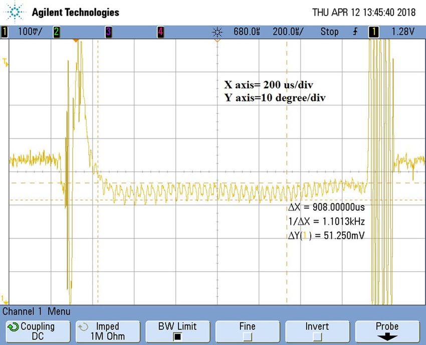
36   Page 6 of 7                                                                        Sådhanå (2020)45:36

   Maintaining RF phase of output pulse for a stable particle    References
beam is important during the accelerator operation [20]. A
phase detector based on Analog Devices make AD8302 IC             [1] Tokuchi A, Kamitsukasa F, Furukawa K, Kawase K, Kato R,
was used to measure the ‘in pulse’ and ‘pulse to pulse’               Irizawa A, Fujimoto M, Osumi H, Funakoshi S, Tsutsumi R,
phase variation of the klystron output power. The card                Suemine S, Honda Y and Isoyama G 2015 Development of a
provides a resolution of 10 mV/° for phase change and has             high-power solid-state switch using static induction thyris-
a range of 0°–180°. The output signal of the card has been            tors for a klystron. Nucl. Instrum. Methods Phys. Res. A 769:
                                                                      72–78
measured on a Digital Storage Oscilloscope (DSO). The IC
                                                                  [2] Shidara T, Anami S, Fukuda S, Saito Y, Honma H, Tanaka J,
utilizes a multiplier type phase detector to which two
                                                                      Horikoshi G and Abchiche A 1989 Klystron modulators for
amplitude limited signals from logarithmic amplifiers are             the KEK 2.5 GeV linac, Nucl. Instrum. Methods Phys. Res. A
fed, resulting in accurate phase detection over a wide power          279: 423–432
range. Unlike conventional modulators the flat top region is      [3] Shrivastava P, Mulchandani J and Sahni V C 2008 Devel-
not ripple free due to the inherent characteristic of the             opment of all solid state bouncer compensated long pulse
converter type modulator. Lower ripple will be possible at            modulators for LEP 1 MW klystrons to be used for LINAC4
the cost of higher value of output filter capacitance but will        project at CERN, In: Proceedings of XIV linear accelerator
increase the stored energy in the system [15]. The output             conference, 29 September–3 October 2008, Victoria, British
RF phase within the pulse has been measured in a single               Columbia, Canada, p. 984
pulse to observe the phase variation A peak to peak vari-         [4] Glasoe G N and Lebacqz J V (Eds) 1946 Pulse generators.
ation of ±2.5° was observed within the flat top portion of            New York: Dover Publications, Inc
                                                                  [5] Gold S L 2000 Thyaratron-PFN, IGBT hybrid, and direct
the pulse as shown in figure 9. Further to this experiment a
                                                                      switched modulator R&D As its effects klystron protection,
study of the phase stability was also observed over hun-
                                                                      In: Proceedings o IEEE twenty fourth international power
dreds of pulses using persistence mode of the Digital                 modulators symposium, Norfolk, VA, USA, 26–29, June,
Storage Oscilloscope (DSO). Similar result of ±2.5° was               2000
observed even in that case same pulse to pulse phase sta-         [6] Zeng R, Johansson A J, Rathsman K and Molloy S 2012
bility being shown in figure 10. During all the experiments,          Influence of the droop and ripple of modulator on klystron
RF input to the klystron tube was kept slightly in over-              output, ESS AD technical note ESS/AD/0033, 23 February
driven condition to ensure the operation of the tube in               2012
saturation region.                                                [7] Roth I S, Torti R, Gaudreau M P J and Kempkes M A 2007 A
                                                                      high-voltage hard-switch modulator for the International
                                                                      linear collider, In: IEEE Proceedings of PAC07, Albu-
                                                                      querque, New Mexico, USA, 25–29, June
                                                                  [8] Patel P J, Thakur D P, Gupta L N, Patel V B, Tripathi V,
4. Conclusion
                                                                      Singh N P and Baruah U K 2009 In: Proceedings series of
                                                                      international topical meeting on nuclear research applica-
A 1 MW pulsed RF test stand has been successfully                     tions and utilization of accelerators, 4–8 May 2009, Vienna,
developed and tested. Using the test stand, performance of            AT/P5-16
1 MW, CW klystron under pulsed operating condition has            [9] Yellamraju S S S and Kulkarni S V 2013 J. Fusion Eng. Des.
been studied and presented. The details of various subsys-            88: 868
tems of RF test stand have been described. The RF output         [10] Reass W A, Baca D M, Doss J D, Grrible R F and North W R
power of the klystron amplifier and its relationship with             2002 In: Proceedings of Japan–US symposium on pulsed
cathode voltage and drive frequency has been studied and              power and plasma applications, Kailua-Kona, Hawaii, USA,
presented. The variation of beam current with respect to              4–8 Aug
cathode voltage is presented. The RF output phase variation      [11] Anderson D A 2009 Developments in solid-state modulator
of ±2.5° within the pulse has been achieved and pulse to              technology towards high availability, In: Proceedings of
                                                                      PAC09, Vancouver, BC, Canada, 4–8 May
phase stability over hundreds pulses are also of the same
                                                                 [12] Reghu T, Mandloi V and Shrivastava P 2014 Development
order. The RF test stand can also be used to test various RF
                                                                      of a 33 kV, 20 A long pulse converter modulator for high
components of particle accelerators.                                  average power klystron. Rev. Sci. Instrum. 85:
                                                                      055102-1–055102-6
                                                                 [13] Acharya M and Shrivastava P 2018 A 100 kV, 20 A, 1 ms
                                                                      long pulse solid-state Marx modulator for klystron. Nucl.
Acknowledgements                                                      Instrum. Methods Phys. Res. A 905: 96–103
                                                                 [14] Acharya M and Shrivastava P 2016 Design and development
The authors would like to thank Dr. P. A. Naik, Director,             of a prototype 25 kV, 10 A long pulse Marx modulator for
RRCAT and Mr. S.C.Joshi, Director, Proton Accelerator                 high power klystron. Rev. Sci. Instrum. 87:
Group for their keen interest and constant support; Mr.               025114-1–025114-6
Rajkumar Namdeo for technical assistance; Mr.                    [15] Reghu T, Mandloi V and Shrivastava P 2018 A solid-state
M. Acharya and Mr. Deodatta Baxy for useful suggestions.              converter topology, -100 kV, 20 A, 1.6 ms, modulator for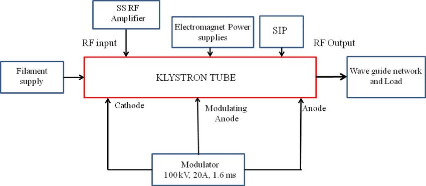
Sådhanå (2020)45:36                                                                         Page 7 of 7    36

     high average power klystron amplifier. IEEE Trans. Plasma       [18] Technical manual of low voltage power supplies 2007 NCN
     Sci. 46(10): 3700–3707                                               1050-35 MOD, 14488-02-01, FuG Elektronik GmbH,
[16] Reghu T, Mandloi V and Shrivastava P 2016 Compact high               Germany
     voltage, high peak power, high frequency transformer for        [19] Gilmour A S Jr 2011 Klystrons, travelling wave tubes,
     converter type modulator applications. Rev. Sci. Instrum. 87:        magnetrons, crossed-field amplifiers, and gyratrons. Artech
     045109-1–045109-6                                                    House, Norwood, MA, USA
[17] TH 2089 CW Klystron data sheet of Thales Electron               [20] Seol K-T 2015 RF phase stability in the 100-MeV proton
     Devices, UTH 2089, 1986 France, November                             linac operation. J. Korean Phys. Soc. 66: 345–348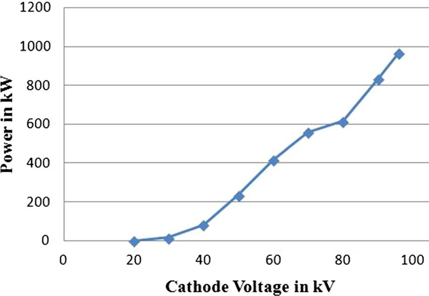
You can also read