Monolithic CMOS ASIC Developments - CERN Indico
←
→
Page content transcription
If your browser does not render page correctly, please read the page content below
Monolithic CMOS ASIC
       Developments
       11th "Trento" Workshop on Advanced Silicon Radiation Detector
       Talk: HVCMOS 1 / 153
       SLAC National Accelerator Laboratory
       P. Caragiulo*, C. Tamma, X. Xu, B. Markovic, J. Segal, A. Dragone,
       M. Breidenbach, C. Kenney, D. Su, P. Grenier
       University of California Santa Cruz - H. Grabas, V. Fadeyev, A. Grillo
       Karlsruhe Institute of Technology - I. Peric
(* pietroc@slac.stanford.edu)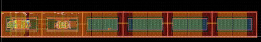
Outline

      •   Monolithic CMOS ASIC
      •   Motivations
      •   CHESS-2 : CMOS HV Evaluation for Strip Sensors
      •   COOL-1: CMOS fOr Outer Layers ASIC
      •   KPiXM: ECal read-out of Silicon Detector for ILC

                                                             2
Monolithic CMOS ASIC

                      AMS 0.35μm HV

           Sensor and read-out on the same substrate.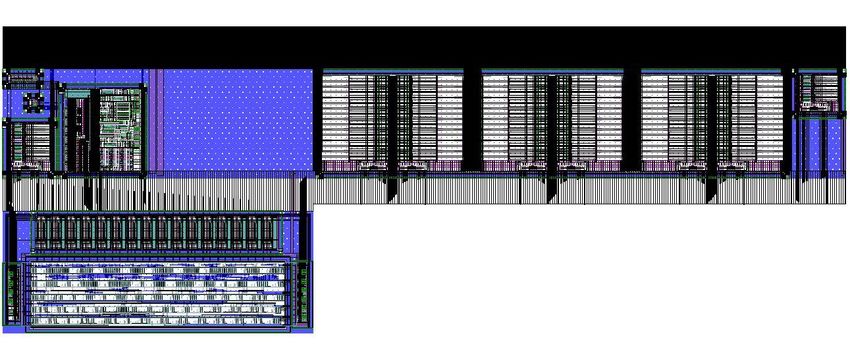
Motivations from a Science perspective

Monolithic technologies have the potential for providing higher granularity, thinner,
intelligent detectors at lower overall cost:
  •   Significantly lower material budget
        - eliminate the need for bump bonding or other challenging interconnect
        methods
        - can be thinned to less than 100um
  •   Smaller pixel size
       - not limited by bump bonding
  •   Lower costs
        - can be implemented in standard commercial technologies
                                        Hybrid         Depleted MAPS
                                                       HVCMOS                 HRCMOS
                    collection speed    fast (drift)   fast (partial/drift)   fast (drift)
                    cost                high           low                    low
                    material            high           low                    low
                    pixel size          medium         small                  small
                    signal              high           low                    high
                    In pix processing   high           Medium/high            high

                                                                                             4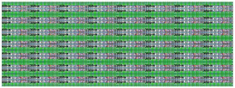
Monolithic technologies for Particle Physics Application

We have an interest in monolithic technologies for applications in Particle
Physics:
 •   ATLAS Strips (CHESS2 in collaboration with UCSC)
 •   ATLAS Outer Pixels (COOL)
 •   ILC SiD Tracker and Ecal (KPiXM)

                                                                              5
CHESS2 - Objectives

• Demonstrate HVCMOS as a viable solution for ATLAS strip
  detector.
 • Record hits on full reticle sensor 128 strips – 32 sub-pixels
 • Amplify, filter and discriminate signal
 • Encode hit position in sensor and send to external readout electronics

• Further investigate performances of HVCMOS MAPS sensors
 • Size close to final sensor : test beams, module assembly, etc..
 • Evaluate sensors with different substrate resistivity 20, 50-100, 200-300,
     600-2000 Ohm-cm.
 •   Study radiation hardness using test structures.
 •   Characterize the pixel arrays with different methods, include edge-TCT
     and beam tests
 •   Large scale effects: common noise, cross-talk, power drops etc..
CHESS2 - Specifications

                                   Specs                   Comments

Substrate resistivity              20Ohms to 1000Ohms      Minimal MIP from from 1500e to
                                                           4000e
Substrate high voltage bias        120V                    40% more charge vs 60V

Pixel size                         40µm x 630µm            400fF det. capacitance

Number of pixel per strip          32

Number of strips                   128                     Factor ~2 improvement in r-phi resol.

Timing resolution                  25ns

Maximum number of hits per strip   1 + flag

Maximum number of hits per 128     8
strips
Readout speed                      320MHz

Number of wire bonds               28/128strips (data only) x5 reduction

Additional constraint              Rad-hard design         Periphery: dead area 4mm - shorter
                                                           strips
CHESS2: Strip sensor size

                          630µm
128 Strip
  5mm

                                              40µm

                            32 pixels/Strip
                                  2cm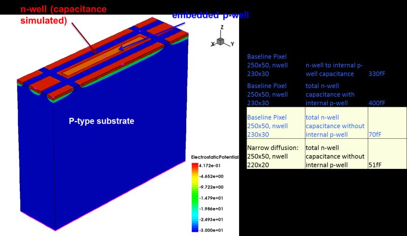
CHESS2: ASIC Architecture

               Column Decoder

                                                                                      Matrix

                                                                       Global DACs
                                                                                     Pointers

                                                                                                 SACI
                                                                                      Control
                                                                                       Logic

                                              Row Decoder
                           Half Comparator,                                           Global
        128 x 32                                               Hit
                            Latch & Strip                                            Registers
         pixels                                             Encoding
                               encoding

                                                                       Serializer
                                                                                      LVDS TX/RX

                                     Acquisition
                                     Encoding
                                     Configuration and Calibration
                                     Read-out

                                                                                                        9
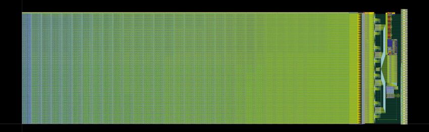
CHESS2 Floor Plan

               Pixels – Row, Column selectors

                    Columns Selector

                                                Rowss Selector
                    Pixels

                       2cm                                       4mm
CHESS2 Floor Plan
Strip Encoding
Strip
EncodingCHESS2 Floor Plan
8 Hit Encoding Logic & Memories
8 Hits
Selection
and memoriesCHESS2 Floor Plan
SACI – Registers – Current sources
SACI &
Current sourcesCHESS2 Floor Plan
Serializer – LVDS TX/RX
Serializer & LVDS TX/RX
14CHESS2: Pixel
Injection IFB
RowENB RAMWrEn
ColENB
3.3
1.8 Th
Load 1/2
Casc 1/2/4/8
Comp
InSF
InCHESS2: Pixel periphery schematic
Strip
• Encode the column address of the first hit and raise a flag if a double hit has occurred on the
same strip
16CHESS2: Pixel Layout – 630µm x 40µm
• Amplifier
• Half comparator
• Charge injection
• Pixel Selection
• Comparator Trimming Memory
• 6 connected NWELLs
• 50% diode fraction
• P-contact around each NWELL
• 120V rulesCHESS2: Simulated Pixel Behavior
DC Response Gain SNR
1MIP@ 20Ω
1MIP@ 600Ω
Equivalent charge at
different substrate
resistivity
75mV @ 20Ω 10 @ 20Ω
~270mV/fC
200mV @ 600Ω 40 @ 600Ω
TRAN Response
Less than 10ns walk time
~10ns peak timeCHESS2: Strip Encoding
Hit address & Flag Hit/No Hit
(6 bits)
1 hit per strip + flag in case of multiple hits. 5 + 1 bit
8 hits maximum per 128 strips. 7 bitCHESS2: Hit Encoding – Fast Skip Concepts
Output bus 8x13b
Strip
or Hit payload
add skip address
add or skip
add or skip 1
add or skip
add or skip
add or skip
add or skip
add or skip
add or skip
add or skip 2
add or skip 3
add or skip
add or skip
add or skip
add or skip
add or skip
Memory
• Adder value used to multiplex data on 8 buses
• Overflow protection in 3b adder: 8 hits maximum
• Adder are slow (up to 1ns in worst case speed)
• Huge load on the bit lines (127 switch off-capacitance + 5mm line capacitance)CHESS2: Hit Encoding – Fast Skip Concepts
Write Memory
+1
25ns
SKIP
Bit line settling
time
Write BitCHESS2: Hit Encoding – Fast Skip Concepts
Write Memory
500ps +1
25ns
150ps
SKIP
4ns Bit line settling
time
300ps Write Bit
• Time to get the bit lines ready is based on number of hits
• Can be as high as 64ns if are all hits.
We are interested in the first 8 hits so the worst case using this
architecture is when we have no hit on the first 120 rows and hit on
the last 8 rows -> 22nsCHESS2: Hit Encoding – Fast Skip Concepts
reset
Write Memory
500ps +1
25ns
150ps
SKIP
4ns Bit line settling
time
300ps Write Bit
• Time to get the bit lines ready is based on number of hits
• Can be as high as 64ns if are all hits.
We are interested in the first 8 hits so the worst case using this
Avoid ghost from previous cycle
architecture is when we have no hit on the first 120 rows and hit on
introducing a reset phase
the last 8 rows -> 22nsCHESS2: Hit Encoding – Fast Skip Concepts
2x Find first 8 hits in 32 rows (2 stage in a
Find first 8 hits in 128 rows
pipeline-like behavior)
Memory
11 x 8b
Memory
11 x 8b
Serializer
Memory
13 x 8b
Serializer
Memory
11 x 8b
Memory
11 x 8b
Worst case
scenario:
22ns 7.6ns
24CHESS2: Fast Adder x32 (Layout)
600 µm
1280 µm
Bus Line
Adders Selector
Bus Lines
25CHESS2: LVDS TX/RX and Sync
Sync pad
13
Serializer
13 13x LVDS Driver 13
320MHz Clock 1 LVDS
Receiver
26CHESS2: Serializer
p
p
p
p
p
p
p
p
s o s o s o s o s o s o s o s o
PISO 1b PISO 1b PISO 1b PISO 1b PISO 1b PISO 1b PISO 1b PISO 1b
- 8 x 13 1bit PISO Cell.
- Parallel input with 25ns period (synchronized to the 40MHz external clock).
- Serial Output has 3.125ns period (synchronized to the 320MHz external clock).
400 µm
150 µm
27SLAC ASIC Control Interface (SACI)
Serial Interface with handshake protocol
Registers
Column
Pointer
Pointer
Global
5 Signals
Row
• 3 shared: saciClk, saciCmd, saciRsp.
• 1 dedicated select line per slave: saciSelL.
• 1 Reset Line (RstL) can be shared with the
ASIC Global Reset.
Control Logic
• Operated between 0V and 3.3V
ADDR[0..11]
DATA[0..31]
CMD[0..6]
•
EXEC
Allows multiple SACI on same bus (parallel
ACK
CLK
R/W
mode).
SLAC ASIC Control
RstL
Interface (SACI)
SACIcmd (serial signal):
saciCmd
saciSelL
saciRsp
saciClk 28SACI – Multiple ASIC connection
SACI Response
RSP
RSP
RSP
RSP
SACI-0 SACI-1 SACI-2 SACI-3
CMD
CMD
CMD
CMD
CLK
CLK
CLK
CLK
SEL
SEL
SEL
SEL
Shared Clock
Shared Command
Sel0
Sel1
Sel2
Sel3
Response line can be shared if only 1 SACI is selected when the command arrives.
29Global Register
Row and Column register for pixel selection
SACI
Command Logic
Digital control signal distribution
700 µm
Control Unit
2000 µm
30Control Unit
Bus to ASIC
Command Decoder Command Logic Rad Hard Bits
+
DataBus to Matrix
Buffers Col
Reg
Pixel Write
Row
Command
Logic
Rad Hard Register
Bits
Bits Reg
+
+
Logic Logic
DATABUS Buffer Logic
SACI System
Internal Bus
SACI Core
CMD, CLK Buffer ADDRESS Buffer
31COOL-1: CMOS fOr Outer Layers ASIC
Can we build a full read-out system that meets the ATLAS pixels requirements (at least for the
outer layers)?
Large Potentials in ATLAS outer pixels 5th and 6th layers!
Tentative goals COOL-1
Pixel size 250x50 µm2
Array 320x80
Full Size reticles
Max. Signal ~10ke-
Effective ENCHR CMOS in LFoundry 0.15μm technology
LF15A is a modular 0.15 μm RF CMOS process, offering up to 6 levels of Al plus thick metal (2 - 6 μm),
optionally a MIM capacitor, a polyimide passivation and I/O voltages of 1.8 V, 3.3V and 5.0 V.
• Substrate resistivity 1-2kΩcm Thinned to 125um:
• Allow isolated NWELL within a DNWELL • full depletion from the back side should be
(Full CMOS) feasible (80V at 2kΩcm)
• Large fill factor ~85% for 50x250 μm^2 • QMIP ~ 10000e-
pixel • Cin ~ 400fF (70fF DNW to SUB, 330fF DNW
• Break down voltage ~120V to PW) for 50x250 μm^2 pixel (worst case)
• Considering sharing a threshold around
1000e- should give us reasonable efficiency.
Required Noise ~100e-
AMS 0.35μm HV
LF 0.15μm HR
33KPiX ASIC: ECal read-out of Silicon Detector (SiD) for ILC
Block diagram of a single channel
1024-channel KPiX
KPiX, An Array of Self Triggered Charge Sensitive Cells Generating Digital Time and Amplitude Information”, D. Freytag. G. Haller, et al. SLAC-PUB-
13462, 2008. 4pp (IEEE NSS Oct 2008)
KPiX, an 1,024 cell ASIC, Design and Performance, accepted for presentation at NSS 2012
34Sensor Traces In present design, metal 2 traces from pixels to pad array run over other pixels: parasitic capacitances cause crosstalk. New scheme has “same” metal 2 traces, but a fixed potential metal 1 trace shields the signal traces from the pixels. The Ecal sensors are large hexagonal silicon sensors with a diameter of about 10cm segmented in little hexagons of ~5mm. KPix is bump bonded in the center and traces running on top of pixels fan out across the entire sensor 35
Major Lessons Learned

• Bump bonding to sensors with Al pads can be very difficult…

     •   Consider sensor foundry build final pad stack.

     •   Don’t dice the sensors until bonding issues are fully controlled.

• EMCal can have huge number of pixels hit simultaneously,
  causing synchronous disturbances as pixels reset…Problem
  understood, small changes in KPiX design.

• Sensors plus ROC’s can have issues with parasitic
  couplings…

                                                                             36
KPiXM
Large Potentials in SiD Trk and Ecal
KPiXM-Trk KPiXM-Cal
Pixel size 50x500 µm2 1000x1000 µm2
Array 200x2400 100x94
Stitched 5x5 Stitched 5x5
Full Size reticles reticles
Max. Signal 1fC 1pC
Effective ENC 4
In pix mem.
depth 1 bucket 16 buckets
ADC resolution 12 bits 12 bits
DC Power cons. ~ 20µW/pix ~ 20µW/pix
Power pulsing Yes Yes
General characteristics
• Amplitude and Timing extraction on N bunches per train in
each pixel (N=1 for the tracker, N=16 for the calorimeter)
• Synchronous (time-variant operation)
• Ultra-large Area beyond reticle size (stitching)
Pixel architecture
• System-on-chip approach (limited IO required
• Platform based design
• Sparse readout
• Power Pulsing
x16 for Cal version
• Calibration per pixel
• Temperature monitoring and tracking
• Auxiliary MonitoringConclusions
• CHESS2 is a full size demonstrator for the strip sensor in
HVCMOS technology. In case of success it would significantly
reduce strip sensor manufacturing cost, material budget, improve
resolution, simplified readout chip.
• Fairly complicated chip with difficult layout and new process,
design time took much longer than expected. In the top level layout
stage and full chip simulations.
• Passive and Active pixel variants for COOL and KPiXM are under
design.
38Acknowledgements
We want to acknowledge for the work on CHESS the contribute of all the people involved in design, test and
characterization of the devices.
Strip CMOS Author list
Affolder0, K.Arndt1, R. Bates2, M. Benoit3, F. Di Bello3, A. Blue2, D. Bortoletto1, M. Buckland0,4, C. Buttar2, P. Caragiulo5, D. Das6, J.
Dopke6, A. Dragone5, F. Ehrler7, V. Fadeyev8, Z. Galloway8, H. Grabas8, I. M. Gregor9, P. Grenier5, A. Grillo8, M. Hoeferkamp10, L.
B. A. Hommels11, T. Huffman1, J. John1, K. Kanisauskas1,2, C. Kenney5, G. Kramberger12, Z. Liang8, I. Mandić12, D. Maneuski2, F.
Martinez-Mckinney8, S. McMahon1,6, L. Meng0,3, M. Mikuž12,13, D. Muenstermann14, R. Nickerson1, I. Peric7, P. Phillips1,6, R.
Plackett1, F. Rubbo5, J. Segal5, S. Seidel10, A. Seiden8, I. Shipsey1, W. Song17, M. Stanitzki9, D. Su5, C. Tamma5, R. Turchetta6, L.
Vigani1, J. Volk8, R. Wang15, M. Warren16, F. Wilson6, S. Worm6, Q. Xiu17, J. Zhang15, H. Zhu17
0University of Liverpool, 1University of Oxford, 2SUPA - School of Physics and Astronomy, University of Glasgow, Glasgow, United Kingdom,
3University of Geneva, Switzerland, 4CERN, European Center for Nuclear Research, 5SLAC National Accelerator Laboratory, 6Rutherford
Appleton Laboratory, Didcot, United Kingdom, 7Karlsruhe Institute of Technology, 8University of California Santa Cruz, Santa Cruz Institute for
Particle Physics (SCIPP), 9Deutsches Elektronen-Synchrotron, 10University of New Mexico, 11Cambridge University, 12Jožef Stefan Institute,
Ljubljana, Slovenia, 13University of Ljubljana, Slovenia, 14Lancaster University, United Kingdom, 15Argonne National Laboratory, 16University
College, London, 17Institute of High Energy Physics, Beijing
And our sponsors:
The research was supported and financed in part by UK Science and Technology Facilities Council (STFC), the Slovenian
Research Agency, the United States Department of Energy, grant DE-FG02-13ER41983, and the SLAC LDRD program. The
research leading to these results has received funding from the European Commission under the FP7 Research Infrastructures
project AIDA, grant agreement no. 262025.
The irradiations with protons were performed at the University of Birmingham MC40 cyclotron, supported by the H2020 project
AIDA-2020, GA number 654168. The irradiations with neutrons were performed at TRIGA reactor in Ljubljana. The authors would
like to thank the crew at the TRIGA reactor in Ljubljana for their help with the irradiation of the detectors, as well as staff at the
Gamma Irradiation Facility of Sandia National Laboratory, especially Dr. M. Wasiolek and Dr. D. Hanson.
39Backup Slides
40KPiX ASIC: ECal read-out of Silicon Detector (SiD) for ILC
32×32 array = 1024 channels
Designed to be
• bump-bonded to a Si sensor, or
• bumped to a hybrid for large area
detectors (RPC’s, GEM’s, etc)
For each channel of the system-on-chip
» 4 samples per train with individual timestamps Block diagram of a single channel
» auto-triggering
» internal per-channel 13-bit ADC
» automatic range switching for large charge depositions (10pC)
» bias current servo for DC coupled sensors
» power cycling: power down during inter-train gaps (20 uW avg for
ILC time structure)
» built-in calibration
» nearest neighbor trigger ability
» high-gain feedback capacitor for tracker application
» dual polarity for GEM and RPC applications
» external trigger for test beam
Digital IP core with serial data IO (only 4 signals) 1024-channel KPiX
0.25μm TSMC
KPiX, An Array of Self Triggered Charge Sensitive Cells Generating Digital Time and Amplitude Information”, D. Freytag. G. Haller, et al. SLAC-PUB-
13462, 2008. 4pp (IEEE NSS Oct 2008)
KPiX, an 1,024 cell ASIC, Design and Performance, accepted for presentation at NSS 2012
41You can also read