ECEN720: High-Speed Links Circuits and Systems Spring 2021 - Lecture 5: Termination, TX Driver, & Multiplexer Circuits Sam Palermo Analog & ...
←
→
Page content transcription
If your browser does not render page correctly, please read the page content below
ECEN720: High-Speed Links
          Circuits and Systems
              Spring 2021

Lecture 5: Termination, TX Driver, & Multiplexer Circuits

                     Sam Palermo
             Analog & Mixed-Signal Center
                 Texas A&M University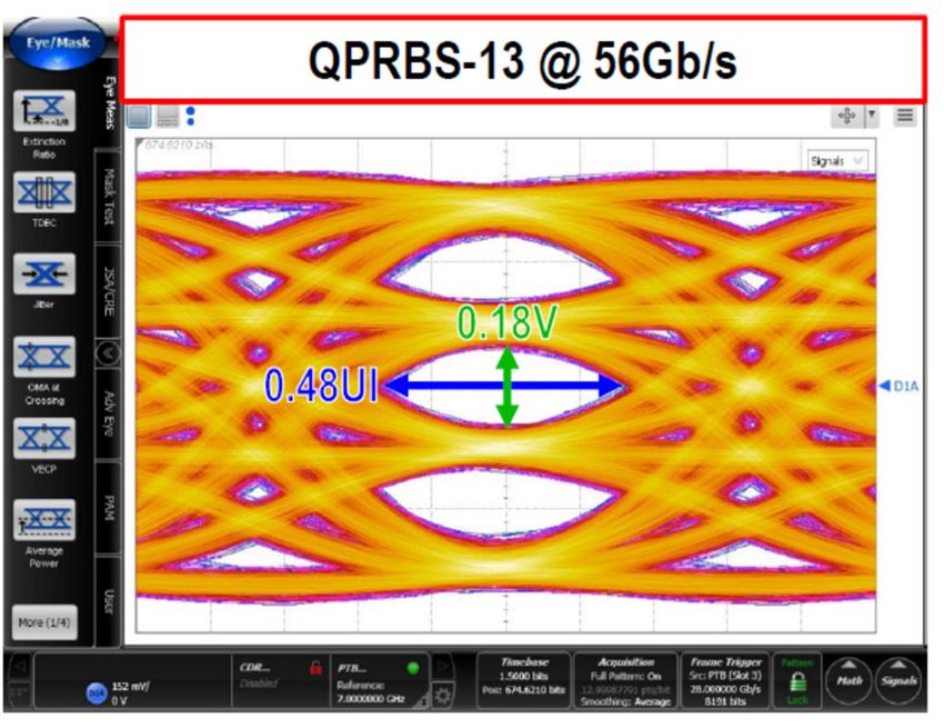
Announcements
• Lab 3 Report and Prelab 4 due Feb. 26

• Reading
  • Papers posted on voltage-mode drivers and high-
    order TX multiplexer circuits

                                                  2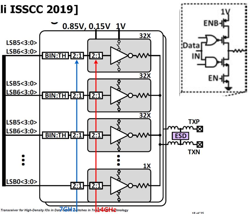
Agenda
• Termination Circuits
• TX Driver Circuits
• TX circuit speed limitations
  • Clock distribution
  • Multiplexing techniques

                                 3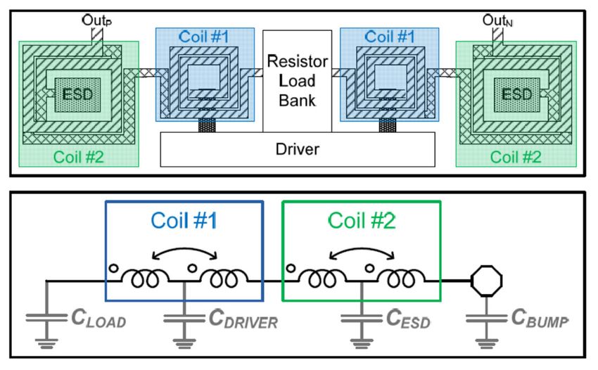
High-Speed Electrical Link System

                                    4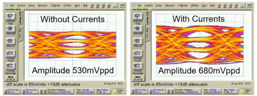
Termination
• Off-chip vs on-chip
• Series vs parallel
• DC vs AC Coupling
• Termination circuits

                         5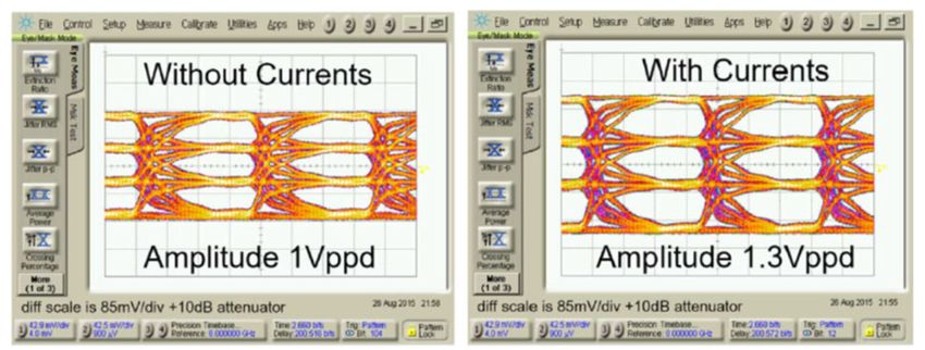
Off-Chip vs On-Chip Termination

                                             [Dally]

• Package parasitics act as an unterminated stub
  which sends reflections back onto the line
• On-chip termination makes package inductance
  part of transmission line
                                                       6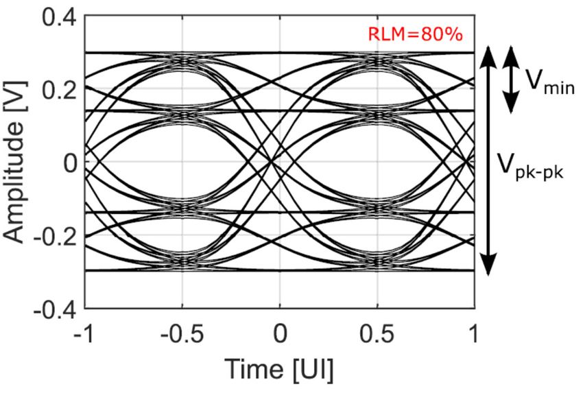
Series vs Parallel Termination
       Series Termination               Parallel Termination

                        Double Termination

• Low impedance voltage-mode driver typically employs
  series termination
• High impedance current-mode driver typically employs
  parallel termination
• Double termination yields best signal quality
   • Done in majority of high performance serial links         7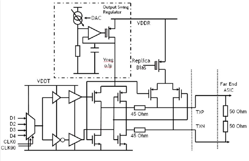
AC vs DC Coupled Termination
• DC coupling allows for
                           RX Common-Mode = IR/2
  uncoded data
• RX common-mode set
  by transmitter signal
  level

• AC coupling allows for   RX Common-Mode = VTT
  independent RX
  common-mode level
• Now channel has low
  frequency cut-off
   • Data must be coded

                                                  8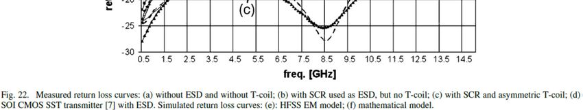
Passive Termination
• Choice of integrated resistors involves trade-offs in manufacturing
steps, sheet resistance, parasitic capacitance, linearity, and ESD
tolerance
• Integrated passive termination resistors are typically realized with
unsalicided poly, diffusion, or n-well resistors
• Poly resistors are typically used due to linearity and tighter
tolerances, but they typically vary +/-30% over process and
temperature
Resistor Options (90nm CMOS)
Resistor Poly N-diffusion N-well
Sheet R (/sq) 9010 30050 450200
VC1(V-1) 0 10-3 8x10⁻³
2-3fF/um2 0.9fF/um2 (area), 0.2fF/um2 (area),
Parasitic Cap
(min L poly) 0.04fF/um (perimeter) 0.7fF/um (perimeter)
9
Active Termination

• Transistors must be used for      [Dally]

  termination in CMOS processes
  which don’t provide resistors
• Triode-biased FET works well
  for low-swing (
Adjustable Termination
• FET resistance is a
function of gate
overdrive
1
RFET
Cox W L VGS Vt [Dally]
• Large variance in FET threshold voltage requires
adjustable termination structures
• Calibration can be done with an analog control
voltage or through digital “trimming”
• Analog control reduces VGS and linear range
• Digital control is generally preferred
11Termination Digital Control Loop
[Dally]
• Off-chip precision resistor is used as reference
• On-chip termination is varied until voltages are within
an LSB
• Dither filter typically used to avoid voltage noise
• Control loop may be shared among several links, but
with increased nanometer CMOS variation per-channel
calibration may be necessary
12High-Speed Electrical Link System
13TX Driver Circuits
• Single-ended vs differential signaling
• Controlled-impedance current & voltage-
mode drivers
• Swing enhancement techniques
• Impedance control
• Pad bandwidth extension
• Slew-rate control
14Single-Ended Signaling
• Finite supply impedance
causes significant
Simultaneous Switching
Output (SSO) noise
(xtalk)
• Necessitates large
amounts of decoupling
capacitance for supplies
and reference voltage
• Decap limits I/O area more
that circuitry
15Differential Signaling
[Sidiropoulos]
• A difference between voltage or current is sent between
two lines
• Requires 2x signal lines relative to single-ended signaling,
but less return pins
• Advantages
• Signal is self-referenced
• Can achieve twice the signal swing
• Rejects common-mode noise
• Return current is ideally only DC
16TX Driver Circuits
• Single-ended vs differential signaling
• Controlled-impedance current & voltage-
mode drivers
• Swing enhancement techniques
• Impedance control
• Pad bandwidth extension
• Slew-rate control
17Controlled-Impedance Drivers
• Signal integrity considerations (min. reflections) requires
50Ω driver output impedance
• To produce an output drive voltage
• Current-mode drivers use Norton-equivalent parallel termination
• Easier to control output impedance
• Voltage-mode drivers use Thevenin-equivalent series
termination
• Potentially ½ to ¼ the current for a given output swing
VZcont 2VSW
D+ D+
D-
D-
18Push-Pull Current-Mode Driver
• Used in Low-Voltage Differential Signals (LVDS) standard
• Driver current is ideally constant, resulting in low dI/dt noise
• Dual current sources allow for good PSRR, but headroom can be a
problem in low-voltage technologies
• Differential peak-to-peak RX swing is IR with double termination
19Current-Mode Logic (CML) Driver
• Used in most high performance serial links
• Low voltage operation relative to push-pull driver
• High output common-mode keeps current source saturated
• Can use DC or AC coupling
• AC coupling requires data coding
• Differential pp RX swing is IR/2 with double termination
20Current-Mode Current Levels
Single-Ended Termination
Vd ,1 I 2 R
Vd ,0 I 2 R
Vd , pp IR
Vd, pp
I
R
Differential Termination
Vd ,1 I 4 2 R
Vd ,0 I 4 2 R
Vd , pp IR
Vd, pp
I
R
21Voltage-Mode Current Levels
Single-Ended Termination
Vd ,1 Vs 2
Vd ,0 Vs 2
Vd , pp Vs
I Vs 2 R
Vd, pp
I
2R
Differential Termination
Vd ,1 Vs 2
Vd ,0 Vs 2
Vd , pp Vs
I Vs 4 R
Vd, pp
I
4R
22Current-Mode vs Voltage-Mode Summary
Driver/Termination Current Level Normalized Current Level
Current-Mode/SE Vd,pp/Z0 1x
Current-Mode/Diff Vd,pp/Z0 1x
Voltage-Mode/SE Vd,pp/2Z0 0.5x
Voltage-Mode/Diff Vd,pp/4Z0 0.25x
• An ideal voltage-mode driver with differential RX
termination enables a potential 4x reduction in
driver power
• Actual driver power levels also depend on
• Output impedance control
• Pre-driver power
• Equalization implementation
23Voltage-Mode Drivers • Voltage-mode driver implementation depends on output swing requirements • For low-swing (
TX Driver Circuits
• Single-ended vs differential signaling
• Controlled-impedance current & voltage-
  mode drivers
• Swing enhancement techniques
• Impedance control
• Pad bandwidth extension
• Slew-rate control

                                            25
High-Swing Transmitter Linearity
• Transmit swings ≥1Vppd
are often needed to
support operation over
high-loss channels
• Reductions in supply
voltages make achieving
this swing with high
linearity difficult
• This is particularly
important with PAM4
modulation
26Parallel Bleeder Current Source
Upadhyaya, VLSI 2016
• Parallel thick-oxide bleeder current source from
1.8V supply raises output common mode
• Achieves >1.2Vppd swing in a 16nm FinFET process
27CML Driver w/ Higher Output Stage Supply
VCC_HV
Kim, ISSCC 2018
Vbias
VCC_NOM
Vcs=~1V
CK90
PGen
D
CK0
ESD ESD
• Higher output stage supply
• Source voltage of switch PMOS transistors remains near 1V
for 10nm reliability
• >1Vppd swing 28Tail-Less Current-Mode Driver
[Steffan ISSCC 2017]
• Bottom transistor driven by full-rate serialized data
• Replica-bias network sets output stage cascode transistors’
gate voltage to achieve the desired output swing
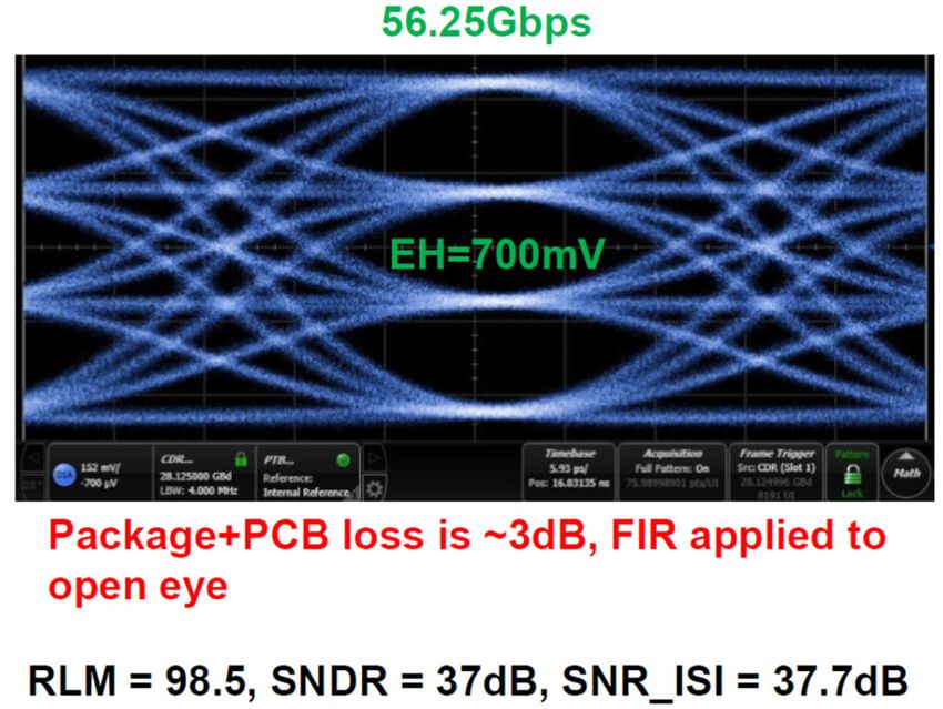
• Achieves 1.2Vppd output swing with 94% RLM
29Voltage-Mode Driver
w/ Level-Shifting Predriver
[Ali ISSCC 2019]
• Predriver uses a 0.85V supply to drive the NMOS and a level
shifted 0.15V GND to drive the PMOS
• Achieves 1Vppd output swing in 7nm CMOS
30Hybrid Voltage-Mode Driver w/ Parallel Current-Mode Segments [Joy ISSCC 2011] • Parallel current-mode output stage provides swing enhancement • Achieves 1.2Vppd output swing in 40nm CMOS 31
PAM4 Hybrid Voltage-Mode Driver
  w/ Parallel Push-Pull Current-Mode Segments
[Bassi JSSC 2016]                                Low-Speed Operation

                                                        45Gb/s

 • Parallel push-pull current sources driven by the MSB & LSB allow for a
   high-swing PAM4 implementation
 • Achieves 1.3Vppd output swing in 1V 28nm CMOS with >94% RLM
                                                                            32
TX Driver Circuits
• Single-ended vs differential signaling
• Controlled-impedance current & voltage-
mode drivers
• Swing enhancement techniques
• Impedance control
• Pad bandwidth extension
• Slew-rate control
33Global Resistor Calibration
[Chan ASSCC 2016]
• Off-chip precision resistor is used as reference
• On-chip termination is varied until voltages are within an LSB
• Dither filter typically used to avoid voltage noise
• In current-mode drivers, this code is used for the nominal
load setting
34Low-Swing VM Driver Impedance Control
[Poulton JSSC 2007]
• A linear regulator sets the output stage supply, Vs
• Termination is implemented by output NMOS transistors
• To compensate for PVT and varying output swing levels, the pre-drive
supply is adjusted with a feedback loop
• The top and bottom output stage transistors need to be sized
differently, as they see a different VOD
354:1 Output Multiplexing Voltage-Mode TX
• Impedance control is
0.65 V achieved independent
VREF ERROR
AMP of the pre-driver supply
4:1 Voltage Mode
Output Driver
Cdec by adding additional
8:4MUX, AND Gate, and Level Shifter
Scalable DVDD VZUP up/down analog-
8x1Gb/s
2Gb/s
Level
controlled NMOS
transistors
Shifter TXP
Txdata 8:4 D Q
DFF 8Gb/s
Q Level TXN
/2 Shifter
CK0/90/
180/270
CP0/90/
180/270
VZDN
• Level-shifting pre-driver
allows for smaller
output transistors
2 Stages PPF CML to CMOS Converter Pulse CP0
Scalable DVDD Generator
I CK0
CKP CP180
Q CK180 CK0
2GHz
CP90
IB CK90 CK0
CKN CK180 CP270
QB CK270
Y.-H. Song, R. Bai, P. Chiang, and S. Palermo, “A 0.47-0.66pJ/bit, 4.8-8Gb/s I/O Transceiver in 65nm-CMOS,” IEEE JSSC, vol. 48,
no. 5, pp. 1276-1289, May 2013. 36Low-Swing Voltage-Mode Driver Analog Impedance Control • Replica global impedance control loop provides analog gate voltages to the additional top/bottom transistors to set the pull-up/down impedance Y.-H. Song, R. Bai, P. Chiang, and S. Palermo, “A 0.47-0.66pJ/bit, 4.8-8Gb/s I/O Transceiver in 65nm-CMOS,” IEEE JSSC, vol. 48, no. 5, pp. 1276-1289, May 2013. 37
High-Swing Voltage-Mode Driver
Impedance Control
               VDD

                 MP

                     Rterm

        In                   Out

                     Rterm

                 MN

• Passive resistors + transistors’ triode resistance
• Output impedance will change due to process variation
• Causes reflection and level mismatch
                                                          38
High-Swing Voltage-Mode Driver
Impedance Control
• Equalization control by setting
the number of segments
connected to each tap
• Termination control by setting
the total number of enabled
segments
• Disadvantages:
• Transistor stacking in full-rate path
• Extra area due to redundant
segments
• Extra power consumption because
pre-driver should be sized to drive
maximum load
• Sensitive to P/N skew variations
39High-Swing Voltage-Mode Driver
Hybrid Impedance Control Scheme
Analog Impedance Loop 75 to 85
driver slices
(10 programmable
slices with NAND and
NOR as pre-driver)
[Chan ASSCC 2016]
• Programmable number of driver slices provides coarse impedance
control to compensate for resistor variations
• Analog impedance loop provides fine impedance control to
compensate for NMOS/PMOS variations
• Measured differential mode return loss meets key protocols
composite return loss mask 40TX Driver Circuits
• Single-ended vs differential signaling
• Controlled-impedance current & voltage-
mode drivers
• Swing enhancement techniques
• Impedance control
• Pad bandwidth extension
• Slew-rate control
41Output Pad Network Challenges • Meeting return loss (S11) spec •
T-Coil Output Stage
                                                 [Kossel JSSC 2008]

• Output T-coil between driver and pad allows for splitting
  of driver, ESD, and pad capacitance
• Provides significant bandwidth enhancement and
  improved return loss                                         43
T-Coil Equations
[Kossel JSSC 2008]
Output Reflection Factor
44T-Coil Wiring & Improvement
[Kossel JSSC 2008]
P1 P3 P2
ESD, no T-coil No ESD or T-coil
Previous SOI design w/ESD
Eq. model
HFSS model
TX w/ T-coil/ESD
• A helical wiring scheme reduces the vertical parasitic fringing capacitance
between layers and improves self-resonance frequency
45Double T-Coil Output Bandwidth Extension
[Steffan ISSCC 2017]
• Double T-coil structure allows
separation of termination
capacitance
• Enhances bandwidth by 1.5X
46-Coil Output Bandwidth Extension
∏-Coil (series-shunt peaking) [Kim ISSCC 2019]
T-Coil (series peaking)
L3 L2 L1 Pad
Cesd1 Cbump
Rterm Cterm Cesd2
Cdrv
TX
• Output -coil provides additional termination
capacitance separation
• Provides additional bandwidth extension at the cost of
slightly degraded return loss
47-Coil Output Bandwidth Extension
Response at TX Pad [Kim ISSCC 2019]
2 1.2
0 RC load
Return loss (dB)
0 T-coil
π-coil
-10 -2 0.8
Voltage (V)
Gain (dB)
-4
-20
-6
Pulse response
0.4
-30 -8
at TX pad
-10
-40 RC load
RC load
0
T-coil
π-coil -12 T-coil
π-coil
-50 -14
1 10 -0.4
1 10 0 40 80 120 160 200
Frequency (GHz)
Frequency (GHz) Time (ps)
Response after 20dB channel
• 1-2dB bandwidth 0 0.3
peaking results in -5 0.25
RC load
T-coil
π-coil
slightly degraded -10
Voltage (V)
0.2
Gain (dB)
-15
return loss, but a -20
0.15
0.1
better pulse -25
0.05
response over a -30
RC load
T-coil 0
-35
low-pass channel -40
π-coil
-0.05
2.86 2.9 2.94 2.98 3.02 3.06
1 10
Time (ns)
Frequency (GHz) 48TX Driver Circuits
• Single-ended vs differential signaling
• Controlled-impedance current & voltage-
mode drivers
• Swing enhancement techniques
• Impedance control
• Pad bandwidth extension
• Slew-rate control
49TX Driver Slew Rate Control
• Output transition times should be controlled
• Too slow
• Limits max data rate
• Too fast
• Can excite resonant circuits, resulting in ISI due to ringing
• Cause excessive crosstalk
• Slew rate control reduces reflections and
crosstalk
50Slew Rate Control w/ Segmented Driver
Current-Mode Driver Voltage-Mode Driver
[Dally] [Wilson JSSC 2001]
• Slew rate control can be implemented with a segmented
output driver
• Segments turn-on time are spaced by 1/n of desired
transition time
• Predriver transition time should also be controlled
51Current-Mode Driver Example
52Voltage-Mode Driver Example
53TX Circuit Speed Limitations
• High-speed links can be limited by both the channel
and the circuits
• Clock generation and distribution is key circuit
bandwidth bottleneck
• Multiplexing circuitry also limits maximum data rate
54TX Multiplexer – Full Rate
• Tree-mux
architecture with
cascaded 2:1 stages
often used
• Full-rate architecture
relaxes clock duty-
cycle, but limits max
data rate
• Need to generate and
distribute high-speed
clock
• Need to design high-
speed flip-flop
55TX Multiplexer – Full Rate Example
• CML logic sometimes
used in last stages [Cao JSSC 2002]
• Minimize CML to save
power
• 10Gb/s in 0.18m CMOS
• 130mW!!
56TX Multiplexer – Half Rate
• Half-rate architecture
eliminates high-speed
clock and flip-flop
• Output eye is sensitive to
clock duty cycle
• Critical path no longer has
flip-flop setup time
• Final mux control is
swapped to prevent
output glitches
• Can also do this in
preceding stages for
better timing margin
57Clock Distribution Speed Limitations
• Max clock frequency that tFO4 in 90nm ~ 30ps
can be efficiently distributed
is limited by clock buffers
ability to propagate narrow
pulses
Clock Amplitude Reduction*
• CMOS buffers are limited to
a min clock period near
8FO4 inverter delays
• About 4GHz in typical 90nm
CMOS
• Full-rate architecture limited
to this data rate in Gb/s
• Need a faster clock use
faster clock buffers
• CML faster slower
• CML w/ inductive peaking *C.-K. Yang, “Design of High-Speed Serial Links in
CMOS," 1998.
58Multiplexing Techniques – ½ Rate
• Full-rate architecture is
limited by maximum clock
frequency to 8FO4 Tb
• To increase data rates
eliminate final retiming and
use multiple phases of a
slower clock to mux data
• Half-rate architecture uses 2
clock phases separated by
180 to mux data
• Allows for 4FO4Tb
• 180 phase spacing (duty cycle)
critical for uniform output eye
592:1 CMOS Mux
*C.-K. Yang, “Design of High-Speed Serial Links in CMOS," 1998.
faster slower
• 2:1 CMOS mux able to propagate a minimum pulse near
2FO4 Tb
• However, with a ½-rate architecture still limited by
clock distribution to 4FO4 Tb
• 8Gb/s in typical 90nm
602:1 CML Mux
[Razavi]
• CML mux can achieve higher speeds due to reduced
self-loading factor
• Cost is higher power consumption that is independent of data
rate (static current)
61Increasing Multiplexing Factor – ¼ Rate
• Increase multiplexing
factor to allow for lower
frequency clock
distribution
• ¼-rate architecture
• 4-phase clock distribution
spaced at 90 allows for
2FO4 Tb
• 90 phase spacing and duty
cycle critical for uniform
output eye
62Increasing Multiplexing Factor – Mux Speed
• Higher fan-in muxes run slower
due to increased cap at mux node
• ¼-rate architecture
• 4:1 CMOS mux can potentially
achieve 2FO4 Tb with low fanout
• An aggressive CMOS-style design has
potential for 16Gb/s in typical 90nmHigh-Order Current-Mode Output-Multiplexed
• 8:1 current-mode mux directly at output pad
• Makes sense if output time constant smaller
than on-chip time constant
out 25 Cout
• Very sensitive to clock phase spacing
• Yang achieved 6Gb/s in 0.35m CMOS
• Equivalent to 33Gb/s in 90nm CMOS (now channel
(not circuit) limited)
Reduction
*C.-K. Yang, “Design of High-Speed Serial Links in CMOS," 1998. 64
Bit Time (FO4)Current-Mode Input-Multiplexed
[Lee JSSC 2000] faster slower
• Reduces output capacitance relative to output-multiplexed
driver
• Easier to implement TX equalization
• Not sensitive to output stage current mismatches
• Reduces power due to each mux stage not having to be
sized to deliver full output current
65Next Time
• Receiver Circuits
• RX parameters
• RX static amplifiers
• Clocked comparators
• Circuits
• Characterization techniques
• Integrating receivers
• RX sensitivity
• Offset correction
66You can also read