EmSTAMP-Neon-CMx Hardware Manual - emtrion
←
→
Page content transcription
If your browser does not render page correctly, please read the page content below
emSTAMP-Neon-CMx
                          Hardware Manual
                             Rev4 / 17.02.2020

                              emtrion GmbH

emSTAMP-Neon-CMx (Rev4)                          1/21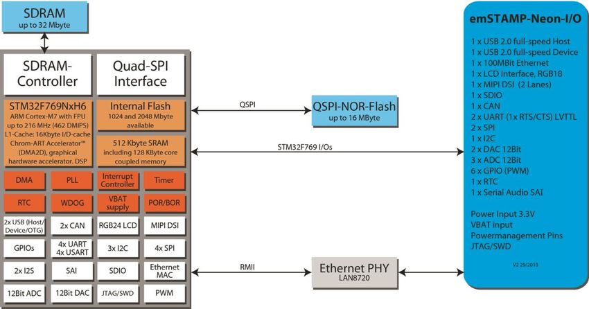
© Copyright 2020 emtrion GmbH

All rights reserved. This documentation may not be photocopied or recorded on any electronic
media without written approval. The information contained in this documentation is subject to
change without prior notice. We assume no liability for erroneous information or its consequences.
Trademarks used from other companies refer exclusively to the products of those companies.

Revision: 4 / 17.02.2020

Rev        Date/Signature     Changes
1          17.07.2018/We      First revision
2          19.09.2019/We      Added new variant emSTAMP-Neon-CM7 with STM32F769 CPU
3          27.09.2019/We      Chapter for USB 2.0 Device added.
                              Chapter for USB 2.0 Host updated.
                              USB-Pins in chapter “castellation connector” updated.
4          17.02.2020/We      Added new variant emSTAMP-Neon-CM479 with STM32F479 CPU.
                              Chapter of recommended footprint updated.

emSTAMP-Neon-CMx (Rev4)                                                                      2/21
Table of Content
1 Introduction................................................................................................................................................................ 4
2 Handling precautions.............................................................................................................................................. 5
3 Block Diagrams .......................................................................................................................................................... 6
3.1 Block Diagram emSTAMP-Neon-CM479 ................................................................................................. 6
3.2 Block Diagram emSTAMP-Neon-CM7 ...................................................................................................... 6
4 Functional Description ........................................................................................................................................... 7
4.1 Module Variants ............................................................................................................................................... 7
4.1.1 Variant emSTAMP-Neon-CM4............................................................................................................ 7
4.1.2 Variant emSTAMP-Neon-CM479....................................................................................................... 7
4.1.3 Variant emSTAMP-Neon-CM7............................................................................................................ 7
4.1.4 Processor Clocks ..................................................................................................................................... 7
4.1.5 Processor features .................................................................................................................................. 8
4.1.6 Boot Configuration ................................................................................................................................ 9
4.2 SDRAM ................................................................................................................................................................. 9
4.3 Serial NOR-Flash ............................................................................................................................................... 9
4.4 Graphic Output .............................................................................................................................................. 10
4.4.1 Color mapping in 16/18bit mode.................................................................................................. 10
4.5 Ethernet ............................................................................................................................................................ 11
4.6 USB 2.0 Host .................................................................................................................................................... 11
4.7 USB 2.0 Device ............................................................................................................................................... 12
4.8 CAN Interface ................................................................................................................................................. 12
4.9 SDIO Interface ................................................................................................................................................ 12
4.10 Serial Ports ....................................................................................................................................................... 13
4.11 I2C Interface ..................................................................................................................................................... 13
4.12 SPI Interfaces .................................................................................................................................................. 13
4.13 Audio Interface .............................................................................................................................................. 14
4.14 GPIOs / PWM ................................................................................................................................................... 14
4.15 Analog to Digital Converter (ADC) ......................................................................................................... 14
4.16 Digital to Analog Converter (DAC) ......................................................................................................... 15
4.17 WKUP Signal ................................................................................................................................................... 15
4.18 Reset .................................................................................................................................................................. 15
4.19 JTAG Debug .................................................................................................................................................... 15
4.20 Power Supply ................................................................................................................................................. 16
4.20.1 +3V3 Supply .......................................................................................................................................... 16
4.20.2 Battery backup voltage VBAT............................................................................................................. 16
5 Castellation Connector ........................................................................................................................................ 17
6 Technical Characteristics .................................................................................................................................... 19
6.1 Electrical Specifications .............................................................................................................................. 19
6.2 Environmental Specifications ................................................................................................................... 19
6.3 Mechanical Specifications ......................................................................................................................... 19
7 Dimensional Drawing .......................................................................................................................................... 20
8 Recommended patterns for soldering........................................................................................................... 20
emSTAMP-Neon-CMx (Rev4) 3/219 References ................................................................................................................................................................ 21
1 Introduction
This document is written for the three available emSTAMP-Neon variants with different CPU types:
• emSTAMP-Neon-CM4 with Cortex-M4 STM32F469NIH6 CPU
• emSTAMP-Neon-CM7 with Cortex-M7 STM32F769NIH6 CPU
• emSTAMP-Neon-CM479 with Cortex-M4 STM32F479NIH6 CPU
For this document the following name convention will be used. The names emSTAMP-Neon-CMx
and STM32-Fxx9NIH6 will be used for both variants.
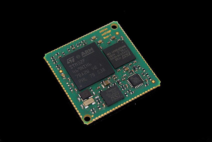
The emSTAMP-Neon-CMx modules are CPU board of emtrions emSTAMP-family, based on the
STM32Fxx9NIH6 microcontroller from STMicroelectronics. The microcontrollers may be clocked up
to 180MHz (emSTAMP-Neon-CM4 and -CM479) and 216MHz (emSTAMP-Neon-CM7). They include
a variety of functions required for IOT or industrial applications.
The CPU boards are designed as a compact module with castellated mounting holes that can be
soldered directly on a baseboard.
The development board emSBC-Neon-CMx with an already equipped emSTAMP-Neon-CMx
module is also available at emtrion. The development board provides power supply and access to
all of the emSTAMP-Neon-CMx interfaces. It is targeted to quickly start into the product
development.
This manual documents the function and available interfaces of the emSTAMP-Neon-CMx
processor module.
emSTAMP-Neon-CMx (Rev4) 4/212 Handling precautions
Please read the following notes prior to installing the processor module. They apply to all ESD
(electrostatic discharge) sensitive components:
• The module does not need any configurations before installing
• The CPU module does not provide any on-board ESD protection circuitry – this must be
provided by the product it is used in.
• Before installing the module it is recommended that you discharge yourself by touching a
grounded object.
• Be sure all tools required for installation are electrostatic discharged as well.
• Before installing (or removing) the module, unplug the power cable from your mains
supply.
• Handle the board with care and try to avoid touching its components or tracks.
emSTAMP-Neon-CMx (Rev4) 5/213 Block Diagrams
3.1 Block Diagram emSTAMP-Neon-CM479
Block Diagram with the available Interfaces of the emSTAMP-Neon-CM479
3.2 Block Diagram emSTAMP-Neon-CM7
Block Diagram with the available Interfaces of the emSTAMP -Neon-CM7
emSTAMP-Neon-CMx (Rev4) 6/214 Functional Description
4.1 Module Variants
4.1.1 Variant emSTAMP-Neon-CM4
The emSTAMP-Neon-CM4 processor module uses the STM32F469NIH6 from STMicroelectronics [2]
which includes an ARM Cortex-M4 with FPU and runs up to 180 MHz clock frequency.
4.1.2 Variant emSTAMP-Neon-CM479
The emSTAMP-Neon-CM4 processor module uses the STM32F479NIH6 from STMicroelectronics [6]
which includes an ARM Cortex-M4 with FPU and runs up to 180 MHz clock frequency.
This CPU has a cryptographic processor and provides hardware acceleration for
• AES 128, 192, 256
• DES and Triple DES,
• HASH (MD5, SHA-1, SHA-224, SHA-256) and HMAC
4.1.3 Variant emSTAMP-Neon-CM7
The emSTAMP-Neon-CM7 processor module uses the STM32F769NIH6 from STMicroelectronics [4]
which includes an ARM Cortex-M7 with double precision FPU (64 bit) and runs up to 216 MHz clock
frequency. The most important changes of the STM32F768NIH6 are listed below:
• L1-cache: 16 KByte I/D cache
• 216 MHz maximum clock frequency
• 462 DMIPS @ 216 MHz
• 512 KByte internal SRAM
• JPEG codec in hardware
• Double precision FPU (64 bit)
4.1.4 Processor Clocks
The processor is clocked by the HSE oscillator, which is connected to a 25 MHz crystal. Several
internal dividers and PLLs multiply the 25 MHz clock input to the internally needed clocks. The
SysClock is set to its maximum speed of 180MHz (emSTAMP-Neon-CM4/CM479) and 216MHz
(emSTAMP-Neon-CM7).
The 25MHz clock signal is used as clock input for the Ethernet-Phy equipped on the emSTAMP-
Neon-CMx module. The 25MHz clock is provided at the Microcontroller Clock Output pin (MCO1) of
the processor.
A 32.768 KHz crystal is connected to the Low Speed External oscillator (LSE) of the processor. Its
main application is to generate the clock for the RTC of the processor.
More information about the clock system is described in the chapter “Reset and Clock Control
(RCC)” of the Reference manuals of STMicroelectronics [1] and [3].
emSTAMP-Neon-CMx (Rev4) 7/214.1.5 Processor features
In addition to the CPU core, the processors provide a lot of functionality. The following features are
provided by the emSTAMP-Neon-CMx modules:
• SDRAM controller
• QSPI-interface for serial-NOR-Flash
• Ethernet 10/100Mbit
• 1x USB 2.0 host in full-speed mode
• 1x USB 2.0 device in full-speed mode
• 1x JTAG debug interface
• 1x LCD controller with 18-bit RGB interface for TFT displays up to 1024x768 (XGA)
• 1x CAN controller
• 1x SDIO controller
• 1x Sound Interface with I²S format
• 2x UART interface (1x with RTS/CTS)
• 2x SPI interface
• 1x I2C Interface
• 3x ADCs with 12-bit resolution
• 2x DAC with 12-bit resolution
• 6x GPIOs with PWM-functionality
• Real time clock
• System reset and wake-up control
emSTAMP-Neon-CMx (Rev4) 8/214.1.6 Boot Configuration The STM32Fxx9 offers three boot modes which are selected by the two CPU pins BOOT[1:0]. The different boot modes are shown in the table below: BOOT1 BOOT0 Boot mode 0 0 Booting from flash memory 0 1 Factory programmed Bootloader is executed 1 0 Booting from flash memory 1 1 Booting from SRAM On the emSTAMP-Neon-CMx module the two boot configuration pins BOOT[1:0] are both connected to a 1k pull-down resistor. By this the default boot mode of the CPU is booting from flash memory. To be able to change the boot mode of the CPU, the pins BOOT[1:0] are connected to the castellated mounting holes of the module. Signal Module pin CPU pin BOOT_0 14 BOOT0 BOOT_1 15 PB2_BOOT1 4.2 SDRAM The emSTAMP-Neon-CMx CPU module provides 32MByte SDRAM as main memory. The RAM is connected via a 16bit wide data bus und may be clocked up to 90MHz. This memory can be used as framebuffer by the LCD controller of the CPU. Please contact emtrion GmbH, if you require a smaller RAM size. 4.3 Serial NOR-Flash A serial NOR-Flash with QSPI-Interface and a memory size of 16MByte is integrated on the CPU module. The memory is connected to Bank1 of the QUADSPI interface. Please contact emtrion GmbH, if you require a smaller flash size. Signal Module pin CPU pin QUADSPI_BK1_IO0 - PF8 QUADSPI_BK1_IO1 - PD12 QUADSPI_BK1_IO2 - PF7 QUADSPI_BK1_IO3 - PF6 QUADSPI_BK1_NCS - PB6 QUADSPI_CLK - PF10 emSTAMP-Neon-CMx (Rev4) 9/21
4.4 Graphic Output
On the emSTAMP-Neon-CMx module the LCD controller of the processor operates in 18-bit or 16-
bit RGB mode and it can drive TFT displays with resolutions up to 1024 x 768 (XGA). The pixel clock
for the display data can be generated by the internal PLLSAI_R.

The following table describes the function of the data and control lines from the STM32Fxx9 LTDC
controller.

Signal            Description
LTDC_R[7:2]       6 color data RED
LTDC_G[7:2]       6 color data GREEN
LTDC_B[7:2]       6 color data BLUE
LTDC _VSYNC       Vertical synchronization signal
LTDC _HSYNC       horizontal synchronization signal
LTDC _DE          Data enable signal, if active color data are valid
LTDC _CLK         Display clock

4.4.1 Color mapping in 16/18bit mode
The following table shows the RGB colour mapping on the TCDC_X[xx] pins available at the
castellated mounting holes on the edge of the CPU module.

LTDC_X[xx]         Module pin          CPU pin         RGB565 (16bit)       RGB666 (18bit)
LTDC _R2              29                 PJ1                 -                   R0
LTDC _R3              30                 PJ2                R0                   R1
LTDC _R4              31                 PJ3                R1                   R2
LTDC _R5              32                 PJ4                R2                   R3
LTDC _R6              33                 PJ5                R3                   R4
LTDC _R7              34                 PG6                R4                   R5
LTDC _G2              78                PI15                G0                   G0
LTDC _G3              79                PG10                G1                   G1
LTDC _G4              80                PJ13                G2                   G2
LTDC _G5              81                 PH4                G3                   G3
LTDC _G6              82                PI11                G4                   G4
LTDC _G7              83                 PB5                G5                   G5
LTDC _B2              85                PJ14                 -                   B0
LTDC _B3              86                PJ15                B0                   B1
LTDC _B4              87                 PK3                B1                   B2
LTDC _B5              88                 PI5                B2                   B3
LTDC _B6              89                 PK6                B3                   B4
LTDC _B7              90                 PK7                B4                   B5
LTDC _VSYNC           11                PI13
LTDC _HSYNC           10                PI12
LTDC _DE              9                  PK7
LTDC _CLK             12                PI14

emSTAMP-Neon-CMx (Rev4)                                                                      10/21
4.5 Ethernet
The emSTAMP-Neon-CMx module provides an Ethernet interface with up to 100BASE-TX full
duplex. The Ethernet RMII interface of the STM32Fxx9 CPU is connected to the external PHY
LAN8720A from Microchip. The PHY address is set to 0.

A 25MHz clock is generated by the STM32Fxx9 on its microcontroller clock output (MCO1 available
at pin PA8) and connected to the XTAL1/CLKIN of the PHY. The PYH operates in the
REFCLOCK_OUT mode, i.e. the reference clock is sourced at the nINT/REFCLOCK pin of the PHY.

The reset input nRST of the PHY is controlled via the PC0 of the STM32Fxx9. An external 10k pull-
down resistor is connected to this signal to hold the PHY in reset during start-up of the CPU.

The PHY LAN8720A is integrated on the CPU module so that an Ethernet Jack (with integrated
magnetics) may be directly connected to the modules Ethernet pins ETH_RDP/ETH_RDM and
ETH_TDP/ETH_TDM which are available at the castellated mounting holes of the module. An
appropriate 1:1 transformer with a 100nF capacitor to GND and a 3.3V supply at each center tap pin
must be added externally. Link or traffic indication signals for additional LEDs are not provided.

Signal               Module pin           CPU pin
ETH_RDP                 28                   -
ETH_RDM                 27                   -
ETH_TDP                 25                   -
ETH_TDM                 24                   -
MCO1                     -                  PA8
PHY_nRST                 -                  PC0

4.6 USB 2.0 Host
The USB 2.0 Host interface is connected to the USB_OTG_HS interface of the STM32Fxx9 and
operates in full-speed mode. The pin PH10 of the STM32Fxx9 processor is used as active low USB
Host Power Enable output (USB USB_OTG_HS_VBUS_EN#). The pin PH8 of the CPU is the
corresponding overcurrent input (USB_OTG_HS_OC#) of the USB Host interface.

Signal                      Module pin       CPU pin
USB_OTG_HS_OC#                 41              PH8
USB_OTG_HS_VBUS_EN#            42             PH10
USB_OTG_HS_DM                  43             PB14
USB_OTG_HS_DP                  44             PB15

emSTAMP-Neon-CMx (Rev4)                                                                      11/21
4.7 USB 2.0 Device
The USB 2.0 Device interface is connected to the USB_OTG_FS interface of the STM32Fxx9 and
operates in full-speed mode. The signal USB_OTG_FS _VBUS at module pin 65 is for the VBUS
detection of the Up-stream port.

Note: maximum input voltage for USB_OTG_FS _VBUS is 4.0V if the emSTAMP-Neon is not
powered and connected to an active USB-Host. STMicroelectronics proposes a resistor divider to
limit the maximum voltage of this pin. For Details please refer to chapter 3.1.1 of application note
AN4879 [5] from STMicroelectronics.

Signal                       Module pin       CPU pin
USB_OTG_FS_VBUS                 65              PA9
USB_OTG_FS_DM                   67             PA11
USB_OTG_FS_DP                   68             PA12

4.8 CAN Interface
The STM32Fxx9 provides the Basic Extended CAN peripheral (bxCAN) to interface the CAN network.
The bxCAN is compliant to the CAN protocol specification 2.0 Part A and B. The LVTTL transmit and
receive signals of the CAN channel are directly connected to the castellated mounting holes of the
module and supports Bit rates of up to 1 Mbit/s.

Signal                Module pin             CPU pin
CAN1_TX                  7                     PB9
CAN1_RX                  8                     PI9

4.9 SDIO Interface
The STM32Fxx9 includes an SDIO interface to connect MultiMediaCards, SD memory cards and
SDIO cards. The SDIO interface allows data transfer of up to 50MHz and supports SD V2.0, SDIO V2.0
and MMC V4.2. The SDIO interface is connected with four data lines to the castellated mounting
holes of the module.

Signal                 Module pin          CPU pin
SDIO_CMD                    58               PD2
SDIO_CD#                    59              PA10
SDIO_D0                     60               PC8
SDIO_D1                     61               PC9
SDIO_D2                     62              PC10
SDIO_D3                     63              PC11
SDIO_CK                     64              PC12
The active low signal for card-detect (SDIO_CD#) is connected to 10k pull-up resistor on the CPU
module.

emSTAMP-Neon-CMx (Rev4)                                                                        12/21
4.10 Serial Ports
The STM32Fxx9 provides up to 8 serial ports. The ports USART2 and USART3 are directly connected
as LVTTL signals to the castellated mounting holes of the module. Both ports support a maximum
baud rate of 2.81 Mbit/s (with oversampling rate 16). USART2 additionally provides hardware
control lines RTS and CTS.

The following table shows the usage of the available USARTs:

Signal                Module pin          CPU pin
USART2_RX                74                 PD6
USART2_TX                75                 PD5
USART2_CTS               76                 PD3
USART2_RTS               77                 PD4
USART3_RX                39                PB11
USART3_TX                40                PB10

4.11 I2C Interface
Up to three I2C bus interface are available at the STM32Fxx9. The interface I2C1 is directly
connected as LVTTL signals to the castellated mounting holes of the module. The I2C1 is equipped
with 2k2 pull-up resistors and supports standard (up to 100KHz) and fast mode (up to 400KHz).
I2C1 also support SMBus 2.0/PMBus.

Signal                Module pin          CPU pin
I2C1_SDA                 92                 PB7
I2C1_SCL                 91                 PB8

4.12 SPI Interfaces
The STM32Fxx9 provides up to 6 SPIs. On the emSTAMP-Neon module two interfaces SPI2 and SPI5
are connected to the castellated mounting holes. SPI5 can communicate at up to 45Mbit/s and
SPI2 up to 22.5Mbit/s.

SPI5 does not have a hardware chip select (SPI5_NSS) pin connected to the mounting holes of the
module. Use a GPIO to generate the chip select signal by software control.

The following table shows the usage of the available SPIs:

Signal                Module pin          CPU pin
SPI2_MOSI                47                 PI3
SPI2_MISO                48                 PC2
SPI2_SCK                 49                 PI1
SPI2_NSS                 50                 PI0
SPI5_MOSI                36                 PF9
SPI5_MISO                38                 PH7
SPI5_SCK                 37                 PH6

emSTAMP-Neon-CMx (Rev4)                                                                   13/21
4.13 Audio Interface
The STM32Fxx9 offers a Serial Audio Interface (SAI) with two independent sub-blocks. The SAI
supports audio protocols like I2S, PCM/DSP, TDM and SPDIF.

On the emSTAMP-Neon-CMx module the sub-block SAI-A of the STM32Fxx9 is connected to the
mounting holes. A master clock output signal is also connected.

The clock for the Serial Audio Interface is derived from the main PLL (PLLM) and therefore it has a
small deviation to the desired audio frequency. The audio PLL (PLLI2S) can be used to minimize the
frequency error. For example a sample rate of 44.1 KHz will have an error of 0,04 %.

Signal               Module pin           CPU pin
SAI1_FS_A               3                   PE4
SAI1_SCK_A              4                   PE5
SAI1_SD_A               5                   PE6
SAI1_MCLK_A             6                   PE2

4.14 GPIOs / PWM
The emSTAMP-Neon-CMx module offers six GPIO on its mounting holes.

As a feature the six channels of the Advanced-Control timer TIM8 are available as alternative port
functions for these pins. The timer TIM8 can be used to generate three-phase PWM motor control
signal with complementary outputs and programmable dead times.

Signal                Module pin       CPU pin
GPIO1/TIM8_CH1N          51             PH13
GPIO2/TIM8_CH1           52              PC6
GPIO3/TIM8_CH2N          53             PH14
GPIO4/TIM8_CH2           54              PC7
GPIO5/TIM8_CH3N          55             PH15
GPIO6/TIM8_CH3           56              PI7

4.15 Analog to Digital Converter (ADC)
The STM32Fxx9 provides three independent analog to digital converter with 12 bit resolution. On
the castellated mounting holes of the emSTAMP-Neon-CMx module, 3 pins are connected to the 3
ADCs of the CPU. The reference voltage for the three analog to digital converter (VREF+) is set to
3.3V.

Signal             Module pin         CPU pin
ADC1_IN9              23                PB1
ADC2_IN6              21                PA6
ADC3_IN3              22                PA3

emSTAMP-Neon-CMx (Rev4)                                                                      14/21
4.16 Digital to Analog Converter (DAC)
The STM32Fxx9 provides two independent digital to analog converter channels with 12 bit
resolution to generate two analog voltage outputs. The input voltage VREF+ of the DAC is set to 3.3V

Signal             Module pin         CPU pin
DAC_OUT1              19                PA4
DAC_OUT2              20                PA5

4.17 WKUP Signal
The WKUP Signal may be used to wake the CPU from standby mode (if enabled). If enabled, the
WKUP-pin is connected to an internal pull-down resistor. The CPU wakes up from standby mode by
a rising edge on the WKUP-Pin. The WKUP-Pin should be driven by open drain/collector outputs, or
connected to GND through a switch. If unused, leave this pin open.

Signal             Module pin         CPU pin
SYS_WKUP              18                PA0

4.18 Reset
The STM32Fxx9 has an internal power supply supervisor, which includes an integrated power-on-
reset (POR) and a power-down reset (PDR). On the emSTAMP-Neon module the POR and PDR
circuitry is always enabled by setting the PDR_ON pin of the CPU to high.

The module provides a STM32_RES# pin to which an active low external reset signal may be
applied to generate a reset of the CPU. This pin is directly connected to the RES# pin of the
STM32Fxx9 and has an external pull-up resistor and a 100nF capacitor. The STM32_RES# pin should
be driven by open drain/collector outputs, or connected to GND through a switch. If unused, leave
this pin open.

Signal             Module pin         CPU pin
STM32_RES#            17               RST#

4.19 JTAG Debug
For programming and debugging the STM32Fxx9 offers two interfaces:

   •   Serial Wire Debug (SWD)
   •   JTAG Debug

Both interfaces are available via the same pins on the castellated mounting holes of the module.

Signal                 Module pin          CPU pin
JTAG_TMS/SWDIO            69                PA13
JTAG_TCLK/SWCLK           70                PA14
JTAG_TDI                  71                PA15
JTAG_TDO                  72                 PB3
JTAG_TRST#                73                 PB4

emSTAMP-Neon-CMx (Rev4)                                                                       15/21
4.20 Power Supply
Supply              Direction           Vmin                 Vtyp                Vmax
+3V3                to module           3.10V                3.3V                3.50V
VBAT                to module           1.65V                                    3.60V

4.20.1 +3V3 Supply
The emSTAMP-Neon module will be powered by a single +3V3 supply. No additional supplies are
required to use the basic functionality of the module.

4.20.2 Battery backup voltage VBAT
By connecting the VBAT supply pin of the STM32Fx68 to a battery or another voltage source, the
internal RTC and/or the backup SRAM can be supplied when the 3.3V supply is turned off. For
details of current consumption in battery backup mode, please refer to the datasheets [2] and [4].

emSTAMP-Neon-CMx (Rev4)                                                                      16/21
5 Castellation Connector
For the placement and the orientation of the 92 castellated mounting holes of the emSTAMP-Neon
module, please refer to chapter “Dimensional Drawing”.

Abbreviations:

RFU      reserved for further use

AI       analogue input
AO       analogue output
I        digital input
O        digital output
I/O      digital bidirectional
O(OD)    digital open drain output

PU xK    x KΩ pullup resistor
PD xK    x KΩ pulldown resistor
SR xR    x Ω series resistor
IPU xK   processor internal x KΩ pullup resistor
IPD xK   transistor internal x KΩ pulldown resistor

In the following table the castellated mounting holes are referred to as “Module Pins”.

Module Pin             Signal         CPU Pin    Direction   Termination
    1                   VDD             VDD           -
    2                    VSS             VSS          -
    3               SAI1_FS_A            PE4        I/O
    4              SAI1_SCK_A            PE5        I/O
    5               SAI1_SD_A            PE6        I/O
    6             SAI1_MCLK_A            PE2         O
    7                CAN1_TX             PB9         O
    8                CAN1_RX             PI9          I        PU 10K
    9                LTDC_DE             PK7         O
   10             LTDC_HSYNC            PI12         O
   11             LTDC_VSYNC            PI13         O
   12               LTDC_CLK            PI14         O
   13                    VSS             VSS          -
   14                 BOOT_0           BOOT0          I         PD 1K
   15                 BOOT_1         PB2/BOOT1        I         PD 1K
   16                   VBAT            VBAT          -
   17              STM32_RES#           NRST          I        PU 10K
   18               SYS_WKUP         PA0/WKUP         I
   19               DAC_OUT1             PA4        AO
   20               DAC_OUT2             PA5        AO
   21               ADC2_IN6             PA6         AI
   22               ADC3_IN3             PA3         AI
   23               ADC1_IN9             PB1         AI
   24                ETH_TDM             PA7          -
   25                ETH_TDP             PC1          -
   26                    VSS             VSS          -
   27               ETH_RDM              PA2          -
   28                ETH_RDP             PA1          -
   29                LTDC_R2             PJ1         O
   30                LTDC_R3             PJ2         O
   31                LTDC_R4             PJ3         O
   32                LTDC_R5             PJ4         O
   33                LTDC_R6             PJ5         O

emSTAMP-Neon-CMx (Rev4)                                                                   17/21
34 LTDC_R7 PG6 O 35 VSS VSS - 36 SPI5_MOSI PF9 O 37 SPI5_SCK PH6 O 38 SPI5_MISO PH7 I 39 USART3_RX PB11 I 40 USART3_TX PB10 O 41 USB_OTG_HS_OC# PH8 I 42 USB_OTG_HS_VBUS_EN PH10 O 43 USB_OTG_HS_DM PB14 I/O 44 USB_OTG_HS_DP PB15 I/O 45 VSS VSS - 46 VDD VDD - 47 SPI2_MOSI PI3 O 48 SPI2_MISO PC2 I 49 SPI2_SCK PI1 O 50 SPI2_NSS PI0 O 51 GPIO1/TIM8_CH1N PH13 I/O 52 GPIO2/TIM8_CH1 PC6 I/O 53 GPIO3/TIM8_CH2N PH14 I/O 54 GPIO4/TIM8_CH2 PC7 I/O 55 GPIO5/TIM8_CH3N PH15 I/O 56 GPIO6/TIM8_CH3 PI7 I/O 57 VSS VSS - 58 SDIO_CMD PD2 O PU 10K 59 SDIO_CD# PA10 I/O PU 10K 60 SDIO_D0 PC8 I/O PU 47K 61 SDIO_D1 PC9 I/O PU 47K 62 SDIO_D2 PC10 I/O PU 47K 63 SDIO_D3 PC11 I/O PU 47K 64 SDIO_CK PC12 O SR 33R 65 USB_OTG_FS_VBUS PA9 AI 66 VSS VSS - 67 USB_OTG_FS_DM PA11 I/O 68 USB_OTG_FS_DP PA12 I/O 69 SYS_JTMS-SWDIO PA13 I/O PU 10K 70 SYS_JTCK-SWCLK PA14 O PD 10K 71 SYS_JTDI PA15 I PU 10K 72 SYS_JTDO-SWO PB3 O 73 SYS_JTRST PB4 O PU 10K 74 USART2_RX PD6 I 75 USART2_TX PD5 O 76 USART2_CTS PD3 I 77 USART2_RTS PD4 O 78 LTDC_G2 PI15 O 79 LTDC_G3 PG10 O 80 LTDC_G4 PJ13 O 81 LTDC_G5 PH4 O 82 LTDC_G6 PI11 O 83 LTDC_G7 PB5 O 84 VSS VSS - 85 LTDC_B2 PJ14 O 86 LTDC_B3 PJ15 O 87 LTDC_B4 PK3 O 88 LTDC_B5 PI5 O 89 LTDC_B6 PK5 O 90 LTDC_B7 PK6 O 91 I2C1_SCL PB8 O(OD) PU 2K2 92 I2C1_SDA PB7 I/O(OD) PU 2K2 emSTAMP-Neon-CMx (Rev4) 18/21
6 Technical Characteristics

6.1 Electrical Specifications
 Supply voltage          3.3V, +/-5%

 Current consumption     up to 360mA (emSTAMP-Neon-CM4)
                         up to 480mA (emSTAMP-Neon-CM7)

6.2 Environmental Specifications
 Operating temperature
 Standard:                0 ... +70°C
 Storage temperature     -10 ... +85°C

 Relative humidity        0 ... 95 %, non-condensing

6.3 Mechanical Specifications
 Weight                  3g

 Board                   FR-4

 Dimensions              28.0 mm x 28.0 mm x 2.5 mm

emSTAMP-Neon-CMx (Rev4)                                   19/21
7 Dimensional Drawing
28,0 mm
22,0 mm
3,0 mm 3,0 mm
Pin69 Pin47
Pin46
Pin70
22,0 mm
28,0 mm
Pin92
Pin24
Pin1 Pin23
Top View on the assembly side.
8 Recommended patterns for soldering
Top View on the assembly side.
emSTAMP-Neon-CMx (Rev4) 20/219 References
[1] RM0386
Reference manual
STM32F469xx and STM32F479xx
advanced ARM®-based 32-bit MCUs
DocID026744 Rev 3, January 2017
STMicroelectronics
[2] STM32F469xx
Datasheet
DocID028196 Rev 4, March 2017
STMicroelectronics
[3] RM0410
Reference manual
STM32F76xxx and STM32F77xxx
advanced ARM®-based 32-bit MCUs
Rev 4, March 2018
STMicroelectronics
[4] STM32F76xxx
Datasheet
DocID029041, Rev 6, September 2017
STMicroelectronics
[5] AN4879
Application Note USB hardware and PCB guidelines
Rev 4, December 2018
STMicroelectronics
[6] STM32F479xx
Datasheet
DS11118 Rev 5, May 2018
STMicroelectronics
emSTAMP-Neon-CMx (Rev4) 21/21You can also read