Fast Flip-Chip Pin-Out Designation Respin by Pin-Block Design and Floorplanning for Package-Board Codesign
←
→
Page content transcription
If your browser does not render page correctly, please read the page content below
Fast Flip-Chip Pin-Out Designation Respin by Pin-Block Design and
                          Floorplanning for Package-Board Codesign

                                       Ren-Jie Lee, Ming-Fang Lai and Hung-Ming Chen
                                  Department of Electronics Engineering and SoC Research Center
                                         National Chiao Tung University, Hsinchu, Taiwan
                                    rjlee@vda.ee.nctu.edu.tw,{terry,hmchen}@mail.nctu.edu.tw

   Abstract— Deep submicron effects drive the complication in            points in a single layer. However this work only created a topological
designing chips, as well as in package designs and communi-              routing, not precise geometry layout, and only the routability issue
cations between package and board. As a result, the iterative            on PCB is considered. [3] presented a simulated annealing algorithm
interface design has been a time-consuming process. This paper           to find a pin assignment solution which considered the routability
proposes a novel and efficient approach to designating pin-              issue on PGA package and PCB, but no other DSM effects were
out for flip-chip BGA package when designing chipsets. The               considered.
proposed approach can not only automate the assignment of                   Fig. 1(a) shows the typical interface design flow for IC-package-
more than 200 I/O pins on package, but also precisely evaluate           PCB codesign. In general, IC designers finish the pin designation
package size which accommodates all pins with almost no                  based on experience (rule-of-thumb). In order to tradeoff signal
void pin positions, as good as the one from manual design.               performance and package cost, they always take a few weeks to
Furthermore, the practical experience and techniques in de-              modify package size, rework package substrate and PCB layout,
signing such interface has been accounted for, including signal          and rearrange pin-out. This conventional process can not efficiently
integrity, power delivery and routability. This efficient pin-out        estimate an accurate package size during designating pins for flip-
designation and package size estimation by pin-block design              chip BGA and possibly degrade signal performance due to the
and floorplanning provides much faster turn around time, thus            weakness on product experience and basic design concept. Further-
enormous improvement in meeting design schedule. The results             more, these costly rework constantly postpone the schedule of chip
on two real cases show that our methodology is effective in              implementation, thus lengthen the time to market (TTM). Hence
achieving almost the same dimensions in package size, compared           this paper presents a novel approach of designating pin-out to
with manual design in weeks, while simultaneously considering            replace heavy-loaded human design by automation process which
critical issues in package-board codesign. To the best of our            accounts for practical experience and techniques. Fig. 1(b) illustrates
knowledge, this is the first attempt in solving flip-chip pin-out        the proposed approach. Obviously this approach will significantly
placement problem in package-board codesign.                             shorten the runtime throughout the automation process. It can not
                                                                         only automate pin-out designation efficiently, but also optimize
                                                                         package size during design stage, thus reduce the time of iteration.
                        I. I NTRODUCTION                                    The contributions presented in this paper are as follows:
                                                                            • We have designed six signal-pin patterns for pin block con-
   Because of deep submicron (DSM) technology, chips now contain               struction in package design. Signal integrity, power delivery,
more functionality and are being driven to higher performance levels           and routability have been accounted for in those patterns. This
than ever before. Consequently, with more functionality on the                 helps to speed up the process of pin-out designation.
chip, designers have to deal with higher I/O densities, more signals        • We have proposed a near optimal approach to minimize pack-
coming out of a chip and tigher geometries [7]. This leads to the              age size by mathematical (linear) programming formulation.
complication in designing package which accommodates chips, as              • We automate this pin-out designation process for package-
well as the board which accommodates the packages. As a result,                board codesign. The experimetal results show that our solution
the ability to design the chip, the package and surrounding system             can achieve almost the same results as manually designed by
concurrently becomes a primary advantage, but also a chanllenge.               experienced designers, with much less time.
   Recently chip-package codesign has drawn attention under these
                                                                            The remainder of the paper is organized as follows. Section
circumstances, for example [2], [11]. However package-board code-
                                                                         II discusses the flip-chip BGA package design with PCB and
sign, which is definitely not a trivial work, still needs more works,
                                                                         DSM effects consideration, while Section III describes our pin-out
especially under DSM effects. There were several works [4], [12],
                                                                         designation by near optimal planning in package size. Section IV
[3], [8] which are related to package and printed circuit board (PCB)
                                                                         shows the experimental results followed by the conclusion in Section
physical designs. [4] presented a style for ball grid array (BGA)
                                                                         V.
ball-out, but shielding pins used for preventing pin-to-pin crosstalk
were not considered. Moreover, when they try to keep the package
cost small, this style puts a restriction on the maximum package
                                                                             II. P IN - OUT D ESIGNATION BY C ONSIDERING S IGNAL
size. Thus, there will be a limit to the number of BGA balls that
can be used for power delivery, and area for power delivery from          I NTEGRITY AND P OWER D ELIVERY IN PACKAGE -B OARD
motherboard to package. [12] proposed an algorithm which assigned                                   C ODESIGN
and routed the solder bumps of a BGA package to a set of fanout
                                                                            Fig. 2 depicts a sketch of PCB layout. Usually PCB board
                                                                         contains several kinds of components and connectors which are
  This work was partially supported by the National Science Council of   applied to specific interfaces. The length of signal net from package
Taiwan ROC under grant No. NSC 95-2220-E-009-028 and -007.               pin to component or connector on PCB is the primary contributor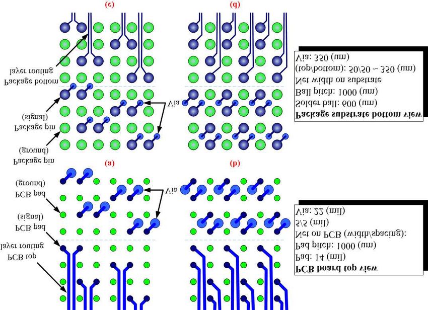
Fig. 3. Simplified cross-section of a flip-chip package which is mounted on
PCB board.
to parasitic inductance. Therefore, package pins will exacerbate
simultaneous switching noise (SSN) by increasing the parasitic
inductance in the signal nets [6]. In order to minimize the physical
length of the package pins thus reduce the total parasitic inductance,
the signal pins should be allocated and restricted in particular region
according to the certain location of corresponding components or
connectors. Fig. 3 shows the simplified cross-section of a flip-chip
package which is mounted on PCB board. Based on experienced
method, the bumps which are beneath the die, located close to die
edge will be routed signal nets through package top layer. On the
contrary, the bumps located around the core of die will be routed
signals through vias and fanned out nets on package bottom layer.
For package pins, which are solder balls, the connected signal nets
are acted according to the same rule to share finite routing resource.
Another crucial factor of successful pin designation is routability.
For routing issue, it should be noted that the net width and spacing
Fig. 1. The typical flow and proposed approach in interface design for on PCB are the critical constraints. The excess row number used
IC-package-board codesign. The focus of this paper is to automate pin-out for placing signal pins will undoubtedly cause routing congestion
designation and to minimize package size during design stage.
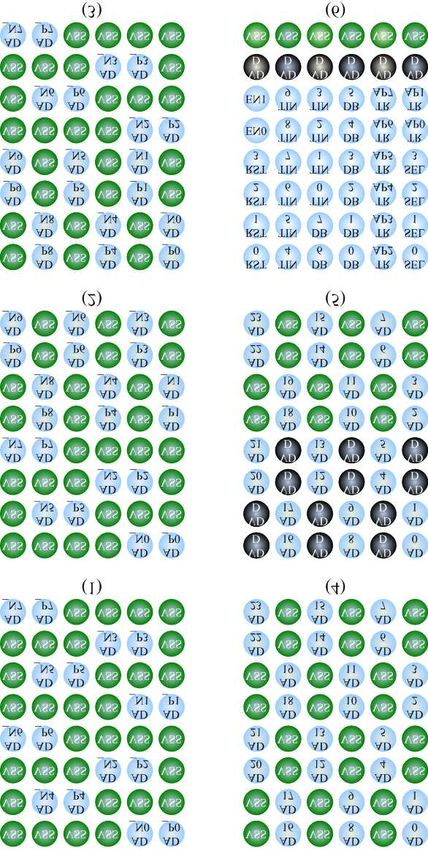
due to restricted area between pins. Fig. 4 demonstrates the routing
pattern on PCB top layer and package bottom layer respectively. For
instance, when the diameter of PCB pad is 14mil (1 mil = 25.4 um),
pad pitch is 1000 um, signal net width is 5mil and net spacing is
5mil on 4 layer PCB board, the space between two pads can only
be penetrated by two nets. That means only three rows of signal
pins can be fanned out nets on PCB top layer. Hence the maximum
row number of outer pins is nine and that of signal pins is seven
(exclusively happened in corners of the package). Fig. 5 lists the
restricted row number of signal pins in different package size.
As for signal integrity, return path inductance should be con-
sidered as well. The unfavorable placement and number of return
path pin, power or ground, will maximize current return loops and
increase return path inductance [6]. This will dramatically degrade
signal integrity and exacerbate radiated emissions. The optimal pin
designation is to place signal pin and power or ground pin proximally
close to each other, so that each signal pin can be tightly coupled
to a return path pin. This will minimize the effect of the return path
inductance. In [5], [10], [9], the effects of shielding, return path
and reference plane are considered in package and PCB designs.
However, the optimal design, in terms of signal integrity concern,
will create such signal-pin blocks which have fewer signal pins
within a large block area.
Fig. 6 illustrates six proposed options of signal-pin pattern for
laying nets out on four layer PCB board. There exists tradeoff
between signal performance and package cost. The first signal-
Fig. 2. A general layout of PCB board. The location of pins on IC package pin pattern exhibits each pair of differential signal which has been
should be restricted in specific regions to meet minimum net-length. surrounded by ground pins. These ground pins can be performed
as adjacent return path pins to minimize total inductance and as
shielding pins to isolate pin-to-pin crosstalk noise. Moreover, the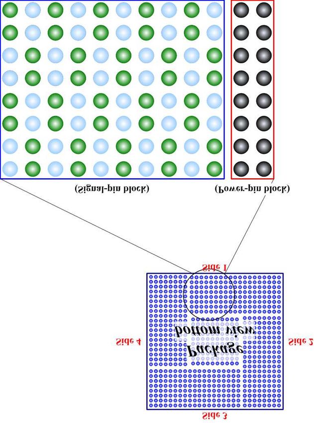
Fig. 4. The routing pattern on PCB top layer (a)(b) and package bottom
layer (c)(d).

Fig. 5. The row number of signal-pin with different package size (PCB
pad=14 mil, pad pitch=1.0 mm, net width=5 mil, net spacing = 5 mil, for
four layer PCB board).                                                    Fig. 6. Six pin patterns presented in this paper. There exists tradeoff
                                                                          between routability and signal integrity concerns. The first pin pattern has
                                                                          better signal integrity, while the sixth one has the most efficient pin
                                                                          designation. In those patterns, AD P0/AD N0 is for differential signal (high
                                                                          speed), AD is for single-ended signal (high speed), and SEL or TRAP in
                                                                          sixth pattern is for single-ended signal (low speed or long-pause signal).
primary concern of differential system is on impendence-matching
of nets. The first pattern has an exclusive advantage of balancing nets
on PCB as well as package substrate layout, shown in Fig. 4(a) and
(c), thus it is optimal for differential signals, from the performance
perspective. The only disadvantage of this pattern is poor pin            integrity, we have proposed six patterns and characterized them in
designation efficiency. In most cases, if the return current flows        Fig. 7. Designers can easily choose a specific pattern along the spec-
on the ground planes, the signal pins should be coupled to the            ification of individual bus, or designers can design pin patterns for
ground pins or vice versa. Furthermore, each signal pin should            their specific purposes. Our automation program can compatible to
be coupled to both one power and one ground pin. If a signal is           other well-defined patterns which has sensible efficiency, routability
coupled to just one power pin or just one ground pin, this case will      and signal integrity.
emerge based on signal type and its configuration. The fourth and             Considering power delivery issue, this paper brings up an idea
fifth signal-pin patterns provide two options for specific bus. The       of establishing a power-pin block. According to the power analysis
fifth pattern has better power delivery characteristic than the fourth    result and production experience, designers can freely define the
one because of locating power pins. These two patterns arrange            demand of power pins for individual signal configuration. While the
pins more efficiently than first pattern, but they both have worse        signal-pin block is constructed, the proposed automation process will
signal integrity on PCB top-layer-routing and package bottom-layer-       create power-pin block then place it adjacent to the related signal-pin
routing due to poor impedance-matching, shown in Fig. 4(b) and            block shown in Fig. 8.
(d). As compared with above-mentioned patterns, the second and
third patterns are the compromises between signal performance and
package cost. The sixth signal-pin pattern is the most efficient pin      III. P IN -O UT D ESIGNATION AUTOMATION BY P IN -B LOCK
designation among all patterns since it contains most signal pins                    C ONSTRUCTION AND F LOORPLANNING
than other patterns. The major disadvantage of this pattern is that it
ignores all signal integrity concerns and can only be applied to test-    A. Pin-Block Construction
in, test-out or long-pulse control signal, which has less sensitivity
in crosstalk.                                                               First, designers determine pin configuration chart based on experi-
    According to the product experience and basic concept of signal       ence about the location of component on PCB and the characteristics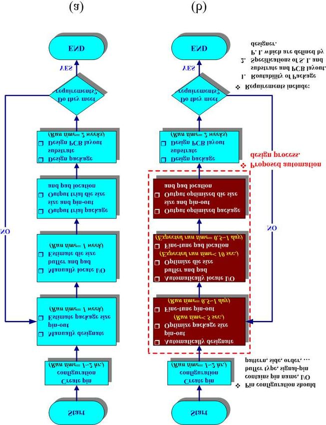
Fig. 7. Characteristics of signal-pin patterns. According to the properties
and requirements of specific signal, we can select a proper pattern for
designating pins.

                                                                              Fig. 10. A minimum package size can be obtained after we designate and
                                                                              floorplan all pin blocks.

                                                                              of each signal group, an example is shown in Fig. 9. In general, it
                                                                              always needs 1 or 2 hours to define the pin configuration for high
                                                                              pin-count chip. From previous discussion, signal integrity, power
                                                                              delivery and routability issues should have been accounted for when
                                                                              signal pins are placed. The pin configuration must include all critical
                                                                              parameters defined for placing signal pins, including the distribution
                                                                              region (side), placement sequence (order), selected signal-pin pattern
                                                                              and the number of power pins. Then both signal-pin block and
                                                                              power-pin block will be built and further grouped into one block Aij
                                                                              for specific bus, where i and j are to represent side and order that
                                                                              blocks are located on and defined in pin configuration by designer.
                                                                              Furthermore designer can acquire parameters wij and hij (w and h
                                                                              represent the width and height of each block respectively).
                                                                                 After finishing the implementation and placement of all blocks,
                                                                              a rough pin designation will be obtained, shown in Fig. 10. At the
                                                                              same time, parameters E1 to E4 can be evaluated from this rough
                                                                              pin designation (E1 to E4 represent the width or height of the empty
                                                                              and excess area in each side of minimum package model).

Fig. 8. A complete pin block includes signal-pin block and its related        B. Minimizing Package Size and Finalizing Pin-out Designa-
power-pin block. It is located on the region close to corresponding           tion by Pin-Block Floorplanning
component on PCB.
                                                                                 The next step is to optimize package size and acquire a feasible
                                                                              pin designation. The following are objective function and constraints,
                                                                              formulated as a linear program. We use an open domain solver to
                                                                              obtain minimize package size:
                                                                                 Minimize
                                                                                                    P       P
                                                                                             f = j=1,3 ( i wji + Ej )hj +
                                                                                                 P         P
                                                                                                    j=2,4 (  i hji + Ej )wj + F

                                                                              subject to
                                                                                                      X                     X
                                                                                       W = w4 +           w1i + E1 = w2 +         w3i + E3        (1)
                                                                                                      i                       i
                                                                                                      X                     X
                                                                                           H = h1 +       h2i + E2 = h3 +         h4i + E4        (2)
                                                                                                      i                      i
Fig. 9. An example of pin configuration chart. In this pin configuration we
can define specific information as inputs of our proposed automated                                          W =H                                 (3)
approach.
                                                                                                    E1 + E2 + E3 + E4 ≥ 0                         (4)
                                                                                                              F ≥c                                (5)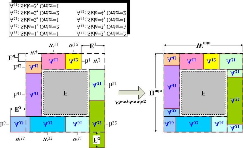
TABLE I                                                                    TABLE II
          T WO INDUSTRIAL BENCHMARKS USED IN THIS PAPER .                            T HE EXPERIMENTAL RESULTSPOF C ASE 1 AND C ASE 2.
           Signal    Pin   Group     Selected    Side   Order   Power-pin                E1     E2    E3      E4      i   Ei     Central     Eval min
            bus      num            signal-pin                   number                                                          p/g pins    package
                                      pattern                                                                                  (F=rowxcol)    (WxH)
 Case 1    Bus#1      66     1           2        1      1        32            Case 1    -3    2      8      -7      0           10x10       26x26
           Bus#2      27     2           3        2      1         8            Case 2    3     -9     -3     12      3           14x14       31x31
           Bus#3      37     3           4        2      2        24
           Bus#4      39     4           1        3      1        N/A
           Bus#5      42     5           1        4      1        24
           Bus#6      58     6           4        4      2        24
 Case 2    Bus#1      66     1           2        1      1        24                                   V. C ONCLUSION
           Bus#2      27     2           3        2      1         8
           Bus#3      95     3           2        2      2        N/A
           Bus#4     100     4           2        3      1         8
                                                                                We have proposed in this paper a novel and efficient approach
           Bus#5      42     5           4        4      1        16         in pin-out designation automation in flip-chip BGA packaging for
           Bus#6      16     6           4        4      2         7         package-board codesign. Due to tradeoff in signal performance
                                                                             and package cost, conventional approach usually take weeks to
                                                                             modify package size and rework package substrate and PCB layout,
                                                                             and rearrange pin-out. The proposed approach can be replaced by
   where w1i ,h1 ,h2i ,w2 ,w3i ,h3 ,h4i ,w4 can be evaluated in the previ-   our efficient methodology. By considering signal integrity, power
ous step, all shown in Fig. 10. F is the center area of BGA package.         delivery, and routability in pin-out block design, our framework
In principal, the power and ground pins are located at the center of         provides good signal quality while achieving close-to-minimum
package and the die is located upon these power and ground pins.             package size, which reduces package cost.
As a result, the heat generated from the die can be transferred out
through these pins [1]. Thus increasing more power and ground pins
located at the center area will improve heat dissipation but enlarge                                        R EFERENCES
the value of F , thereby enlarge the package size. We use (5) to
define the value of F in accordance with physical die size, where             [1] “Designing with High-Density BGA Packages for Altera Devices”.
c is user specified parameter. Use (1) to (3) will restrict the shape             Application Note of Altera Corporation, AN-114-4.0, February 2006.
                                                                              [2] H.-M. Chen, I.-M. Liu, D. Wong, M. Shao, and L.-D. Huang. “I/O
of package to be square. The purpose of (4) is to insure that the
                                                                                  Clustering in Design Cost and Performance Optimization for Flip-Chip
minimum package size can accommodate all pin blocks with almost                   Design”. In Proceedings IEEE International Conference on Computer
no void pin positions.                                                            Design, pages 562–567, 2004.
   After E1 to E4 are obtained, we can easily recognize the position          [3] S.-S. Chen, W.-D. Tseng, J.-T. Yan, and S.-J. Chen. “Printed Circuit
of the empty and excess area in the minimum package. The final                    Board Routing and Package Layout Codesign”. In Proceedings of IEEE
step of proposed methodology is to floorplan pin blocks, which are                Asia-Pacific Conference on Circuits and Systems, pages 155–158, 2002.
to shift the location of pins in the excess area and fill them into the       [4] T.-O. Chong, S.-H. Ong, T.-G. Yew, C.-Y. Chung, and R. Sankman.
adjacent empty area. It can completely eliminate exceed area and                  “Low Cost Flip Chip Package Design Concepts for High Density
                                                                                  I/O”. In Proceedings of IEEE Electronic Componenets and Technology
keep those pins being located around the particular region restricted
                                                                                  Conference, pages 1140–1143, 2001.
in previous step. Fig. 10 shows an example, where there are two               [5] E. Diaz-Alvarez and J. Krusius. “Design, simulation, fabrication,
excess areas occurred in second and third side (upper right and upper             and characterization of package level micro shielding for EMI/EMC
left corners) and two empty areas occurred in first and fourth side               management in BGA environment”. In Proceedings of IEEE Electronic
(bottom right and bottom left corners). Some of the pins in the                   Componenets and Technology Conference, pages 793–798, 2000.
excess areas will be shifted into the empty areas through a simple            [6] S. Hall, G. Hall, and J. McCall. “High-Speed Digital System Design”.
procedure, then acquire an optimized package size, and we finish                  Wiley-Interscience Publication, 2000.
the pin designation process.                                                  [7] J. Mcgrath. “Chip/Package Co-Design: The bridge between chips and
                                                                                  systems”. In Advanced Packaging, June 2001.
                                                                              [8] D. Montuno, Q. Zhang, B. Stacey, W. Chen, V. Chaudhary, D. Poirier,
                                                                                  and T. Mentor. “Towards PCB Physical Design Automation: Archi-
                    IV. E XPERIMENTAL R ESULTS                                    tectural Analysis and Synthesis”. In Proceedings of IEEE Electronic
                                                                                  Componenets and Technology Conference, pages 991–994, 1997.
                                                                              [9] N. Oka, C. Miyazaki, T. Uchida, and S. Nitta. “Effect of a shielding
   We have implemented our methodology in C++ and the platform                    plane connected to ground plane of a PCB in EMI reduction”. In
is on AMD Sempron 1.75GHz with 1GB memory. We use two                             International Symposium on Electromagnetic Compatibility, pages 204–
industrial chipset cases as our benchmarks, shown in Table I,                     207, 1999.
which comes from the pin configuration charts (Fig. 9). Table I,             [10] T. Sudo, Y. Ko, S. Sakaguchi, and T. Tokumaru. “Electromagnetic
Fig. 11 and Fig. 12 show the results of pin-out designation for                   radiation and simultaneous switching noise in a CMOS device packag-
these two benchmarks. Based on Table II which is obtained from                    ing”. In Proceedings of IEEE Electronic Componenets and Technology
linear programming formulation shown in Section III.B, we can get                 Conference, pages 781–785, 2000.
corresponding parameters to floorplan all pin-blocks. The runtime of         [11] J. Xiong, Y.-C. Wong, E. Sarto, and L. He. “Constraint Driven I/O
                                                                                  Planning and Placement for Chip-package Co-design”. In Proceedings
designating pin-out is less than 5 second for both cases. For Case 1,             IEEE Asia and South Pacific Design Automation Conference, pages
our pin-out designation (Fig. 11(b)) is perfectly matched with manual             207–212, 2006.
design (Fig. 11(c)) achieved by an experienced engineer, which spent         [12] M.-F. Yu and W.-M. Dai. “Single-Layer Fanout Routing and Routability
long turn-around time to respin the design (usually weeks). For Case              Analysis for Ball Grid Arrays”. In Proceedings IEEE/ACM Interna-
2, due to more pin numbers in some buses and signal-pin block                     tional Conference on Computer-Aided Design, pages 581–586, 1995.
pattern usage (while pin number is not divisible by 8 will generate
void position), a slightly larger package size (Fig. 12(e)) is achieved,
but still very close to the manual design (Fig. 12(f)).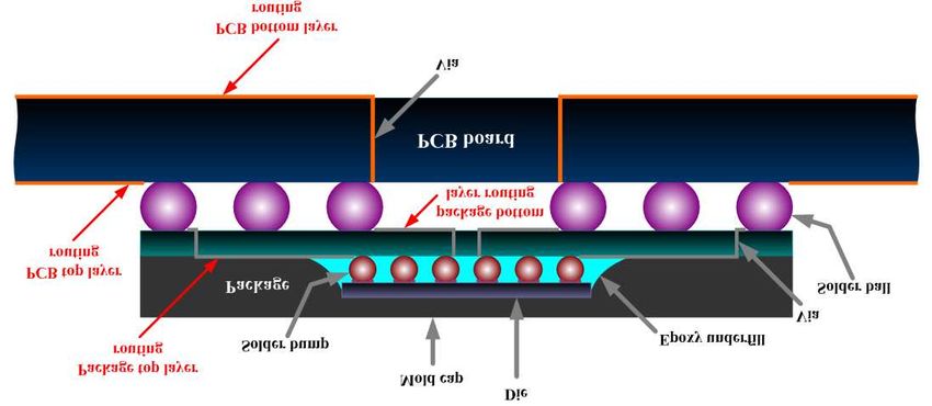
Fig. 11. Experimental results of case 1: (a) Placement of blocks in minimum package evaluation. (b) Sketch of pin-out after floorplanning.(c) Manually
designated pin-out. Our approach can produce the same dimensions as in manual design.

Fig. 12. Experimental results of case 2: (d) Placement of blocks in minimum package evaluation. (e) Sketch of pin-out after floorplanning. (f) Manually
designated pin-out. Our approach can produce a pin designation layout (31x31) very close to the manual one (30x30).
You can also read