AN2834 Application note - How to get the best ADC accuracy in STM32 microcontrollers
←
→
Page content transcription
If your browser does not render page correctly, please read the page content below
AN2834
                                                                       Application note
                                                    How to get the best ADC accuracy
                                                           in STM32 microcontrollers

              Introduction
              STM32 microcontrollers embed advanced 12-bit or 16-bit ADCs (depending on the device).
              A self-calibration feature is provided to enhance ADC accuracy versus environmental
              condition changes.
              In applications involving analog-to-digital conversion, ADC accuracy has an impact on the
              overall system quality and efficiency. To improve this accuracy, the errors associated with
              the ADC and the parameters affecting them must be understood.
              ADC accuracy does not only depend on ADC performance and features, but also on the
              overall application design around the ADC.
              This application note aim is to help understand ADC errors and explain how to enhance
              ADC accuracy. It is divided into three main parts:
              • a simplified description of ADC internal structure to help understand ADC operation and
                related ADC parameters
              • explanations of the different types and sources of ADC errors related to the ADC design
                and to external ADC parameters such as the external hardware design
              • recommendations on how to minimize these errors, focusing on hardware and software
                methods

August 2020                                    AN2834 Rev 5                                            1/58
                                                                                                  www.st.com   1
Contents                                                                                                                        AN2834

Contents

1          General information . . . . . . . . . . . . . . . . . . . . . . . . . . . . . . . . . . . . . . . . . 6

2          ADC internal principle . . . . . . . . . . . . . . . . . . . . . . . . . . . . . . . . . . . . . . . . 6
           2.1      SAR ADC internal structure . . . . . . . . . . . . . . . . . . . . . . . . . . . . . . . . . . . . 6

3          ADC errors . . . . . . . . . . . . . . . . . . . . . . . . . . . . . . . . . . . . . . . . . . . . . . . . 10
           3.1      Errors due to the ADC itself . . . . . . . . . . . . . . . . . . . . . . . . . . . . . . . . . . . 10
                    3.1.1       Offset error . . . . . . . . . . . . . . . . . . . . . . . . . . . . . . . . . . . . . . . . . . . . . . . 10
                    3.1.2       Gain error . . . . . . . . . . . . . . . . . . . . . . . . . . . . . . . . . . . . . . . . . . . . . . . . 12
                    3.1.3       Differential linearity error . . . . . . . . . . . . . . . . . . . . . . . . . . . . . . . . . . . . 13
                    3.1.4       Integral linearity error . . . . . . . . . . . . . . . . . . . . . . . . . . . . . . . . . . . . . . . 14
                    3.1.5       Total unadjusted error . . . . . . . . . . . . . . . . . . . . . . . . . . . . . . . . . . . . . . 16
           3.2      Errors due to the ADC environment . . . . . . . . . . . . . . . . . . . . . . . . . . . . . 17
                    3.2.1       Reference voltage noise . . . . . . . . . . . . . . . . . . . . . . . . . . . . . . . . . . . . 17
                    3.2.2       Reference voltage / power supply regulation . . . . . . . . . . . . . . . . . . . . . 17
                    3.2.3       Reference voltage decoupling and impedance . . . . . . . . . . . . . . . . . . . 18
                    3.2.4       External reference voltage parameters . . . . . . . . . . . . . . . . . . . . . . . . . 18
                    3.2.5       Analog input signal noise . . . . . . . . . . . . . . . . . . . . . . . . . . . . . . . . . . . . 18
                    3.2.6       ADC dynamic range bad match for maximum input signal amplitude . . 18
                    3.2.7       Effect of the analog signal source resistance . . . . . . . . . . . . . . . . . . . . 19
                    3.2.8       Effect of source capacitance and parasitic capacitance of the PCB . . . 20
                    3.2.9       Injection current effect . . . . . . . . . . . . . . . . . . . . . . . . . . . . . . . . . . . . . . 21
                    3.2.10      Temperature influence . . . . . . . . . . . . . . . . . . . . . . . . . . . . . . . . . . . . . . 21
                    3.2.11      I/O pin crosstalk . . . . . . . . . . . . . . . . . . . . . . . . . . . . . . . . . . . . . . . . . . . 22
                    3.2.12      EMI-induced noise . . . . . . . . . . . . . . . . . . . . . . . . . . . . . . . . . . . . . . . . . 22

4          How to get the best ADC accuracy . . . . . . . . . . . . . . . . . . . . . . . . . . . . 23
           4.1      Reduce the effects of ADC-related ADC errors . . . . . . . . . . . . . . . . . . . . 23
           4.2      Minimize ADC errors related to external environment of ADC . . . . . . . . . 23
                    4.2.1       Reference voltage / Power supply noise minimization . . . . . . . . . . . . . 23
                    4.2.2       Reference voltage / Power-supply regulation . . . . . . . . . . . . . . . . . . . . 25
                    4.2.3       Analog-input signal noise elimination . . . . . . . . . . . . . . . . . . . . . . . . . . 25
                    4.2.4       Adding white noise or triangular sweep to improve resolution . . . . . . . . 26
                    4.2.5       Matching the ADC dynamic range to the maximum signal amplitude . . 27

2/58                                                  AN2834 Rev 5
AN2834                                                                                                                   Contents

                  4.2.6       SAR ADC sampling time prerequisites . . . . . . . . . . . . . . . . . . . . . . . . . 29
                  4.2.7       External analog buffer usage . . . . . . . . . . . . . . . . . . . . . . . . . . . . . . . . . 38
                  4.2.8       Source frequency condition vs. source and parasitic capacitors . . . . . . 38
                  4.2.9       Temperature-effect compensation . . . . . . . . . . . . . . . . . . . . . . . . . . . . . 40
                  4.2.10      Minimizing injection current . . . . . . . . . . . . . . . . . . . . . . . . . . . . . . . . . . 40
                  4.2.11      Minimizing I/O pin crosstalk . . . . . . . . . . . . . . . . . . . . . . . . . . . . . . . . . . 40
                  4.2.12      EMI-induced noise reduction . . . . . . . . . . . . . . . . . . . . . . . . . . . . . . . . . 41
                  4.2.13      PCB layout recommendations . . . . . . . . . . . . . . . . . . . . . . . . . . . . . . . . 42
                  4.2.14      Component placement and routing . . . . . . . . . . . . . . . . . . . . . . . . . . . . 44
         4.3      Software methods to improve precision . . . . . . . . . . . . . . . . . . . . . . . . . . 44
                  4.3.1       Averaging samples . . . . . . . . . . . . . . . . . . . . . . . . . . . . . . . . . . . . . . . . 44
                  4.3.2       Digital signal filtering . . . . . . . . . . . . . . . . . . . . . . . . . . . . . . . . . . . . . . . 45
                  4.3.3       FFT for AC measurement . . . . . . . . . . . . . . . . . . . . . . . . . . . . . . . . . . . 46
                  4.3.4       ADC calibration . . . . . . . . . . . . . . . . . . . . . . . . . . . . . . . . . . . . . . . . . . . 47
                  4.3.5       Minimizing internal CPU noise . . . . . . . . . . . . . . . . . . . . . . . . . . . . . . . . 47
         4.4      High impedance source measurement . . . . . . . . . . . . . . . . . . . . . . . . . . . 48
                  4.4.1       ADC input stage problem . . . . . . . . . . . . . . . . . . . . . . . . . . . . . . . . . . . . 48
                  4.4.2       Explanation of the behavior . . . . . . . . . . . . . . . . . . . . . . . . . . . . . . . . . . 49
                  4.4.3       Minimizing additional errors . . . . . . . . . . . . . . . . . . . . . . . . . . . . . . . . . . 50
                  4.4.4       Source of described problem - ADC design . . . . . . . . . . . . . . . . . . . . . . 54

5        Conclusion . . . . . . . . . . . . . . . . . . . . . . . . . . . . . . . . . . . . . . . . . . . . . . . . 56

6        Revision history . . . . . . . . . . . . . . . . . . . . . . . . . . . . . . . . . . . . . . . . . . . 57

                                                   AN2834 Rev 5                                                                  3/58
                                                                                                                                          3
List of tables                                                                                                                    AN2834

List of tables

Table 1.    Minimum sampling time for STM32H7 Series devices (in ns) . . . . . . . . . . . . . . . . . . . . . . 33
Table 2.    ADC SMP selection vs STM32 Series (in ADC clock cycles) . . . . . . . . . . . . . . . . . . . . . . . 34
Table 3.    Rounded minimum sampling time vs resolution
            and maximum error (in ADC clock cycles) . . . . . . . . . . . . . . . . . . . . . . . . . . . . . . . . . . . . . 35
Table 4.    Minimum SMP values vs resolution and maximum error
            (in ADC clock cycles) . . . . . . . . . . . . . . . . . . . . . . . . . . . . . . . . . . . . . . . . . . . . . . . . . . . . . 35
Table 5.    Additional ADC clock cycles due to SMP
            vs resolution and maximum error . . . . . . . . . . . . . . . . . . . . . . . . . . . . . . . . . . . . . . . . . . . . 35
Table 6.    Minimum ADC conversion time (TSMPL + TSAR) vs resolution
            and maximum error (in ADC clock cycles) . . . . . . . . . . . . . . . . . . . . . . . . . . . . . . . . . . . . . 36
Table 7.    Maximum ADC output sampling rate (MSPS)
            vs resolution and maximum error . . . . . . . . . . . . . . . . . . . . . . . . . . . . . . . . . . . . . . . . . . . . 36
Table 8.    Document revision history . . . . . . . . . . . . . . . . . . . . . . . . . . . . . . . . . . . . . . . . . . . . . . . . . 57

4/58                                                      AN2834 Rev 5
AN2834 List of figures
List of figures
Figure 1. Basic schematic of SAR switched-capacitor ADC (example of 10-bit ADC). . . . . . . . . . . . . 6
Figure 2. Sample state . . . . . . . . . . . . . . . . . . . . . . . . . . . . . . . . . . . . . . . . . . . . . . . . . . . . . . . . . . . . . 7
Figure 3. Hold state . . . . . . . . . . . . . . . . . . . . . . . . . . . . . . . . . . . . . . . . . . . . . . . . . . . . . . . . . . . . . . . 7
Figure 4. Step 1: Compare with VREF/2 . . . . . . . . . . . . . . . . . . . . . . . . . . . . . . . . . . . . . . . . . . . . . . . 8
Figure 5. Step 2: If MSB = 0, then compare with ¼VREF . . . . . . . . . . . . . . . . . . . . . . . . . . . . . . . . . . 8
Figure 6. Step 2: If MSB = 1, then compare with ¾VREF . . . . . . . . . . . . . . . . . . . . . . . . . . . . . . . . . . 9
Figure 7. Positive offset error representation . . . . . . . . . . . . . . . . . . . . . . . . . . . . . . . . . . . . . . . . . . . 11
Figure 8. Negative offset error representation . . . . . . . . . . . . . . . . . . . . . . . . . . . . . . . . . . . . . . . . . . 11
Figure 9. Positive gain error representation . . . . . . . . . . . . . . . . . . . . . . . . . . . . . . . . . . . . . . . . . . . . 12
Figure 10. Negative gain error representation . . . . . . . . . . . . . . . . . . . . . . . . . . . . . . . . . . . . . . . . . . . 13
Figure 11. Differential linearity error representation. . . . . . . . . . . . . . . . . . . . . . . . . . . . . . . . . . . . . . . 14
Figure 12. Integral linearity error representation . . . . . . . . . . . . . . . . . . . . . . . . . . . . . . . . . . . . . . . . . 15
Figure 13. Total unadjusted error. . . . . . . . . . . . . . . . . . . . . . . . . . . . . . . . . . . . . . . . . . . . . . . . . . . . . 16
Figure 14. Input signal amplitude vs. ADC dynamic range . . . . . . . . . . . . . . . . . . . . . . . . . . . . . . . . . 19
Figure 15. Analog signal source resistance effect . . . . . . . . . . . . . . . . . . . . . . . . . . . . . . . . . . . . . . . . 20
Figure 16. Analog input with RAIN, CAIN and Cp . . . . . . . . . . . . . . . . . . . . . . . . . . . . . . . . . . . . . . . . . 21
Figure 17. Effect of injection current . . . . . . . . . . . . . . . . . . . . . . . . . . . . . . . . . . . . . . . . . . . . . . . . . . 21
Figure 18. Crosstalk between I/O pins . . . . . . . . . . . . . . . . . . . . . . . . . . . . . . . . . . . . . . . . . . . . . . . . . 22
Figure 19. EMI sources . . . . . . . . . . . . . . . . . . . . . . . . . . . . . . . . . . . . . . . . . . . . . . . . . . . . . . . . . . . . 22
Figure 20. Power supply and reference decoupling for 100- and 144-pin packages . . . . . . . . . . . . . . 24
Figure 21. Power supply decoupling for 36-, 48- and 64-pin packages . . . . . . . . . . . . . . . . . . . . . . . . 25
Figure 22. Simple quasi-triangular source using a microcontroller output . . . . . . . . . . . . . . . . . . . . . . 27
Figure 23. Selecting the reference voltage . . . . . . . . . . . . . . . . . . . . . . . . . . . . . . . . . . . . . . . . . . . . . 28
Figure 24. Preamplification . . . . . . . . . . . . . . . . . . . . . . . . . . . . . . . . . . . . . . . . . . . . . . . . . . . . . . . . . 28
Figure 25. SAR ADC sample conversion process . . . . . . . . . . . . . . . . . . . . . . . . . . . . . . . . . . . . . . . . 29
Figure 26. Simplified external/internal SAR ADC sampling diagram . . . . . . . . . . . . . . . . . . . . . . . . . . 31
Figure 27. Example of SAR ADC input sampling time vs ADC resolution . . . . . . . . . . . . . . . . . . . . . . 32
Figure 28. Example of SAR ADC input sampling time vs accuracy . . . . . . . . . . . . . . . . . . . . . . . . . . . 33
Figure 29. SMP clock cycles vs STM32 Series . . . . . . . . . . . . . . . . . . . . . . . . . . . . . . . . . . . . . . . . . . 34
Figure 30. TSMPL estimation versus ADC frequency and comparison of minimum TSMPL duration
for slow and fast channels with same RAIN/CAIN . . . . . . . . . . . . . . . . . . . . . . . . . . . . . . . 37
Figure 31. TSMPL estimation versus ADC frequency and comparison of minimum TSMPL duration
for fast channels with RAIN/CAIN = 51 Ω/10 pf and 100 Ω/33 pF . . . . . . . . . . . . . . . . . . . 38
Figure 32. Recommended values for RAIN and CAIN vs. source frequency FAIN . . . . . . . . . . . . . . . . . . . . . . 39
Figure 33. Crosstalk between I/O pins . . . . . . . . . . . . . . . . . . . . . . . . . . . . . . . . . . . . . . . . . . . . . . . . . 40
Figure 34. Shielding technique . . . . . . . . . . . . . . . . . . . . . . . . . . . . . . . . . . . . . . . . . . . . . . . . . . . . . . 41
Figure 35. Separating the analog and digital layouts . . . . . . . . . . . . . . . . . . . . . . . . . . . . . . . . . . . . . . 42
Figure 36. Separating the analog and digital supplies . . . . . . . . . . . . . . . . . . . . . . . . . . . . . . . . . . . . . 43
Figure 37. Typical voltage source connection to ADC input . . . . . . . . . . . . . . . . . . . . . . . . . . . . . . . . 48
Figure 38. Noise observed on ADC input pin during ADC conversions . . . . . . . . . . . . . . . . . . . . . . . . 48
Figure 39. ADC simplified schematic of input stage - sample and hold circuit. . . . . . . . . . . . . . . . . . . 49
Figure 40. ADC input pin noise spikes from internal charge during sampling process . . . . . . . . . . . . 49
Figure 41. Effect of sampling time extension . . . . . . . . . . . . . . . . . . . . . . . . . . . . . . . . . . . . . . . . . . . . 50
Figure 42. Charging the external capacitor with too short time between conversions . . . . . . . . . . . . . 51
Figure 43. Implementation of sampling switch . . . . . . . . . . . . . . . . . . . . . . . . . . . . . . . . . . . . . . . . . . . 54
Figure 44. Parasitic capacitances of sampling switch . . . . . . . . . . . . . . . . . . . . . . . . . . . . . . . . . . . . . 55
Figure 45. Parasitic current example inside ADC structure . . . . . . . . . . . . . . . . . . . . . . . . . . . . . . . . . 55
AN2834 Rev 5 5/58
5General information AN2834
1 General information
This application note applies to STM32 Arm®(a)-based microcontrollers.
2 ADC internal principle
2.1 SAR ADC internal structure
The ADC embedded in STM32 microcontrollers uses the SAR (successive approximation
register) principle, by which the conversion is performed in several steps. The number of
conversion steps is equal to the number of bits in the ADC converter. Each step is driven by
the ADC clock. Each ADC clock produces one bit from result to output. The ADC internal
design is based on the switched-capacitor technique.
The following figures (Figure 1 to Figure 6) explain the principle of ADC operation. The
example given below shows only the first steps of approximation but the process continues
till the LSB is reached.
Figure 1. Basic schematic of SAR switched-capacitor ADC (example of 10-bit ADC)
VREF
VIN
Sa
S1 S2 S3 S4 S5 S6 S7 S8 S9 S10 S11
C C/2 C/4 C/8 C/16 C/32 C/64 C/128 C/256 C/512 C/512
Sb A D PR Q ADC Data
CLK
CLR
ADC Clk
ai17097b
1. Basic ADC schematic with digital output.
a. Arm is a registered trademark of Arm Limited (or its subsidiaries) in the US and/or elsewhere.
6/58 AN2834 Rev 5AN2834 ADC internal principle
Figure 2. Sample state
VREF
VIN
Sa
S1 S2 S3 S4 S5 S6 S7 S8 S9 S10 S11
C C/2 C/4 C/8 C/16 C/32 C/64 C/128 C/256 C/512 C/512
Sb A D PR Q ADC Data
CLK
CLR
ADC Clk
VCOMP= 0
2C
VIN
Equivalent circuit: A
ai17098b
1. Sample state: capacitors are charging to VIN voltage. Sa switched to VIN, Sb switch closed during sampling
time.
Figure 3. Hold state
VREF
VIN
Sa
S1 S2 S3 S4 S5 S6 S7 S8 S9 S10 S11
C C/2 C/4 C/8 C/16 C/32 C/64 C/128 C/256 C/512 C/512
Sb A D PR Q ADC Data
CLK
CLR
ADC Clk
VCOMP= –VIN
2C
Equivalent circuit: A
ai17099b
1. Hold state: the input is disconnected, capacitors hold input voltage. Sb switch is open, then S1-S11
switched to ground and Sa switched to VREF.
AN2834 Rev 5 7/58
57ADC internal principle AN2834
Figure 4. Step 1: Compare with VREF/2
VREF
VIN
Sa
S1 S2 S3 S4 S5 S6 S7 S8 S9 S10 S11
C C/2 C/4 C/8 C/16 C/32 C/64 C/128 C/256 C/512 C/512
Sb A D PR Q ADC Data
CLK
CLR
ADC Clk
VCOMP= –VIN+ VREF/2
C
VREF
Equivalent circuit: C A
ai17800b
1. First approximation step. S1 switched to VREF.
Figure 5. Step 2: If MSB = 0, then compare with ¼VREF
VREF
VIN
Sa
S1 S2 S3 S4 S5 S6 S7 S8 S9 S10 S11
C C/2 C/4 C/8 C/16 C/32 C/64 C/128 C/256 C/512 C/512
Sb A D PR Q ADC Data
CLK
CLR
ADC Clk
VCOMP= –VIN+ 1/4 VREF
C/2
VREF
Equivalent circuit: 3C/2 A
ai17801b
1. Compare with ¼VREF; if MSB =1. S1 switched back to ground. S2 switched to VREF.
8/58 AN2834 Rev 5AN2834 ADC internal principle
Figure 6. Step 2: If MSB = 1, then compare with ¾VREF
VREF
VIN
Sa
S1 S2 S3 S4 S5 S6 S7 S8 S9 S10 S11
C C/2 C/4 C/8 C/16 C/32 C/64 C/128 C/256 C/512 C/512
Sb A D PR Q ADC Data
CLK
CLR
ADC Clk
VCOMP= –VIN+ 3/4VREF
3C/2
VREF
Equivalent circuit: C/2 A
ai17802b
1. Compare with ¾VREF; if MSB =0. S1 remained switched to ground. S2 switched to VREF.
AN2834 Rev 5 9/58
57ADC errors AN2834
3 ADC errors
This section lists the main errors that have an effect on A/D conversion accuracy. These
types of errors occur in all A/D converters and conversion quality depends on their
elimination. These error values are specified in the ADC characteristics section of STM32
microcontroller datasheets.
Different accuracy error types are specified for the STM32 ADC. For easy reference,
accuracy errors are expressed as multiples of 1 LSB. The resolution in terms of voltage
depends on the reference voltage. The error in terms of voltage is calculated by multiplying
the number of LSBs by the voltage corresponding to 1 LSB (1 LSB = VREF+/212 or
VDDA/212).
3.1 Errors due to the ADC itself
3.1.1 Offset error
The offset error is the deviation between the first actual transition and the first ideal
transition. The first transition occurs when the digital ADC output changes from 0 to 1.
Ideally, when the analog input ranges between 0.5 LSB and 1.5 LSB, the digital output
should be 1. Still ideally, the first transition occurs at 0.5 LSB. The offset error is denoted by
EO. The offset error can easily be calibrated by the application firmware.
Example
For the STM32 ADC, the smallest detectable incremental change in voltage is expressed in
terms of LSBs:
1 LSB = VREF+/4096 (on some packages, VREF+ = VDDA).
If VREF+ = 3.3 V, the input of 402.8 µV (0.5 LSB = 0.5 × 805.6 µV) should ideally lead to the
generation of a digital output of 1. In practice, however, the ADC may still provide a reading
of 0. If a digital output of 1 is obtained from an analog input of 550 µV, then:
Offset error = Actual transition – Ideal transition
EO = 550 µV – 402.8 µV = 141.2 µV
EO = 141.2 µV / 805.6 µV = 0.17 LSB
When an analog input voltage greater than 0.5 LSB generates the first transition, the offset
error is positive (refer to Figure 7 for an example of positive offset error).
10/58 AN2834 Rev 5AN2834 ADC errors
Figure 7. Positive offset error representation
Digital output
Ideal transfer curve
EO > 0
2
Actual transfer curve
1
0 VAIN
0.5LSB
ai15475b
1. The error offset, EO, is shown in magenta.
When an analog input voltage of less than 0.5 LSB generates the first transition, the offset
error is negative (refer to Figure 8 for an example of negative offset error).
If the analog input voltage (VAIN) is equal to VSSA and the ADC generates a non-zero digital
output, the offset error is negative. This means that a negative voltage generates the first
transition.
Figure 8. Negative offset error representation
Digital output
Ideal transfer curve
EO > 0
Actual transfer curve
2
1
0 VAIN
0.5LSB
ai15476b
1. The error offset, EO, is shown in magenta.
AN2834 Rev 5 11/58
57ADC errors AN2834
3.1.2 Gain error
The gain error is the deviation between the last actual transition and the last ideal transition.
It is denoted by EG.
The last actual transition is the transition from 0xFFE to 0xFFF. Ideally, there should be a
transition from 0xFFE to 0xFFF when the analog input is equal to VREF+ – 0.5 LSB. So for
VREF+= 3.3 V, the last ideal transition should occur at 3.299597 V.
If the ADC provides the 0xFFF reading for VAIN < VREF+ – 0.5 LSB, then a negative gain
error is obtained.
Example
The gain error is obtained by the formula below:
EG = Last actual transition – ideal transition
If VREF+ = 3.3 V and VAIN = 3.298435 V generate a transition from 0xFFE to 0xFFF then:
EG = 3.298435 V – 3.299597 V
EG = –1162 µV
EG = (–1162 µV / 805.6 V) LSB = –1.44 LSB
If a full scale reading (0xFFF) is not obtained for VAIN equal to VREF+, the gain error is
positive. This means that a voltage greater than VREF+ will cause the last transition. Figure 9
shows a positive gain error while Figure 10 shows a a negative gain error.
Figure 9. Positive gain error representation
Digital output
4095
EG > 0
Ideal transfer curve
Actual transfer curve
VAIN
4094.5
LSB
ai5477b
1. The gain error, EG, is shown in magenta.
12/58 AN2834 Rev 5AN2834 ADC errors
Figure 10. Negative gain error representation
Digital output
4095
EG < 0
Ideal transfer curve
Actual transfer curve
VAIN
4094.5
LSB
ai15478b
1. The gain error, EG, is shown in magenta.
3.1.3 Differential linearity error
The differential linearity error (DLE) is the maximum deviation between the actual and ideal
steps. Here ‘ideal’ does not refer to the ideal transfer curve but to the ADC resolution. The
DLE is denoted by ED. It is represented in Figure 11.
ED = Actual step width – 1 LSB
Ideally, an analog input voltage change of 1 LSB should cause a change in the digital code.
If an analog input voltage greater than 1 LSB is required for a change in digital code, a
differential linearity error is observed. The DLE therefore corresponds to the maximum
additional voltage that is required to change from one digital code to the next.
The DLE is also known as the differential non-linearity (DNL) error.
Example
A given digital output should correspond to an analog input range. Ideally, the step width
should be 1 LSB. Let us assume that the digital output is the same over an analog input
voltage range of 1.9998 V to 2.0014 V, the step width will be:
2.0014 V – 1.9998 V = 1.6 mV.
ED is thus the voltage difference between the higher (2.0014 V) and the lower (1.9998 V)
analog voltages minus the voltage corresponding to 1 LSB.
AN2834 Rev 5 13/58
57ADC errors AN2834
Figure 11. Differential linearity error representation
Actual
Digital output Step
width 1LSB
ED > 0
1LSB Actual step width
ED < 0
Ideal transfer curve
Actual transfer curve
VAIN
ai15479b
1. The differential linearity error, ED, is shown in magenta.
If VREF+ = 3.3 V, an analog input of 1.9998 V (0x9B1) can provide results varying between
0x9B0 and 0x9B2. Similarly, for an input of 2.0014 V (0x9B3), the results may vary between
0x9B2 and 0x9B4.
As a result, the total voltage variation corresponding to the 0x9B2 step is:
0x9B3 – 0x9B1, that is, 2.0014 V – 1.9998 V = 1.6 mV (1660 µV)
ED = 1660 µV – 805.6 µV
ED = 854.4 µV
ED = (854.4 µV/805.6 µV) LSB
ED = 1.06 LSB
Let us assume that no voltage greater than 2.0014 V will result in the 0x9B2 digital code
when the step width is less than 1 LSB, ED is negative.
3.1.4 Integral linearity error
The integral linearity error is the maximum deviation between any actual transition and the
endpoint correlation line. The ILE is denoted by EL. It is represented in Figure 12.
The endpoint correlation line can be defined as the line on the A/D transfer curve that
connects the first actual transition with the last actual transition. EL is the deviation from this
line for each transition. The endpoint correlation line thus corresponds to the actual transfer
curve and has no relation to the ideal transfer curve.
The ILE is also known as the integral non linearity error (INL). The ILE is the integral of the
DLE over the whole range.
14/58 AN2834 Rev 5AN2834 ADC errors
Figure 12. Integral linearity error representation
Digital output
4095
EL
2
Actual transfer curve
1
0 VAIN
550 wV 3.298435 V
ai15480b
1. The integral linearity error, EL, is shown in magenta.
Example
If the first transition from 0 to 1 occurs at 550 µV and the last transition (0xFFE to 0xFFF)
occurs at 3.298435 V (gain error), then the line on the transfer curve that connects the
actual digital codes 0x1 and 0xFFF is the endpoint correlation line.
AN2834 Rev 5 15/58
57ADC errors AN2834
3.1.5 Total unadjusted error
The total unadjusted error (TUE) is the maximum deviation between the actual and the ideal
transfer curves. This parameter specifies the total errors that may occur, thus causing the
maximum deviation between the ideal digital output and the actual digital output. TUE is the
maximum deviation recorded between the ideal expected value and the actual value
obtained from the ADC for any input voltage.
The TUE is denoted by ET. It is represented in Figure 13.
The TUE is not the sum of EO, EG, EL, ED. The offset error affects the digital result at lower
voltages whereas the gain error affects the digital output for higher voltages.
Example
If VREF+ = 3.3 V and VAIN = 2 V, the ideal result is 0x9B2. However, if the conversion result
of 0x9B4 is obtained, the deviation may result from the offset since the DLE and ILE errors
occur simultaneously.
TUE = absolute (actual value – ideal case value) = 0x9B4 – 0x9B2 = 0x2 = 2 LSB
Figure 13. Total unadjusted error
Digital output
ET
Ideal transfer curve
Actual transfer curve
VAIN
ai15481b
1. The total unadjusted error, ET, is shown in magenta.
16/58 AN2834 Rev 5AN2834 ADC errors
3.2 Errors due to the ADC environment
3.2.1 Reference voltage noise
As the ADC output is the ratio between the analog signal voltage and the reference voltage,
any noise on the analog reference causes a change in the converted digital value. VDDA
analog power supply is used on some packages as the reference voltage (VREF+), so the
quality of VDDA power supply has influence on ADC error.
For example, with an analog reference of 3.3 V (VREF+ = VDDA) and a 1 V signal input, the
converted result is:
(1/3.3) × 4095 = 0x4D9
However, with a 40 mV peak-to-peak ripple in the analog reference, the converted value
becomes:
(1/3.34) × 4095 = 0x4CA (with VREF+ at its peak).
Error = 0x4D9 – 0x4CA = 15 LSB
The SMPS (switch-mode power supply) usually embeds internal fast-switching power
transistors. This introduces high-frequency noise in the output. The switching noise is in the
range of 15 kHz to 1 MHz.
3.2.2 Reference voltage / power supply regulation
Power supply regulation is very important for ADC accuracy since the conversion result is
the ratio of the analog input voltage to the VREF+ value.
If the power supply output decreases when connected to VDDA or VREF+ due to the loads on
these inputs and to its output impedance, an error will be introduced in the conversion result.
N
V AIN ( 2 – 1 )
-, where N is the resolution of the ADC (in our case N = 12).
Digital code = ---------------------------------
V REF+
If the reference voltage changes, the digital result changes too.
For example:
If the supply used is a reference voltage of 3.3 V and VAIN = 1 V, the digital output is:
12
1 × (2 – 1)
Digital output = ---------------------------------- = 0x4D9
3.3
If the voltage supply provides a voltage equal to 3.292 V (after its output connection to
VREF+), then:
12
1 × (2 – 1)
Digital output = ---------------------------------- = 0x4DC
3.292
The error introduced by the voltage drop is: 0x4DC – 0x4D9 = 3 LSB.
AN2834 Rev 5 17/58
57ADC errors AN2834
3.2.3 Reference voltage decoupling and impedance
The reference voltage source must have a low output impedance to provide a nominal
voltage under various load conditions. Both resistive and inductive parts of the output
impedance are important. During the ADC conversion, the reference voltage is connected to
the switched capacitor network (see Figure 4. and Figure 5.). The capacitors of this network
are charged/discharged from/to a reference voltage in a very short time during successive
approximations (one approximation cycle corresponding to one ADC clock period). The
reference voltage must provide high current peaks to capacitors. Voltages on capacitors
must be stable at the end of each approximation cycle (zero current from the reference
voltage). Therefore, the reference voltage must have a very low output impedance including
low inductance (to provide high current peaks in a very short time). Parasitic inductance can
prevent the charging process from being fully finished at the end of the approximation cycle
or oscillations can appear in the LC circuit (parasitic inductance together with capacitor
network). In this case, the result of the approximation cycle is inaccurate. Correct
decoupling capacitors on the reference voltage located very close to pins provide a low
source impedance.
3.2.4 External reference voltage parameters
In case of usage external source for reference voltage (on VREF+ pin) there are important
parameters of this external reference source. Three reference voltage specifications must
be considered: temperature drift, voltage noise, long term stability.
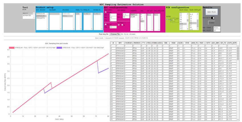
3.2.5 Analog input signal noise
Small but high-frequency signal variation can result in big conversion errors during sampling
time. This noise is generated by electrical devices, such as motors, engine ignition, power
lines. It affects the source signal (such as sensors) by adding an unwanted signal. As a
consequence, the ADC conversion results are not accurate.
3.2.6 ADC dynamic range bad match for maximum input signal amplitude
To obtain the maximum ADC conversion precision, it is very important that the ADC dynamic
range matches the maximum amplitude of the signal to be converted. Let us assume that
the signal to be converted varies between 0 V and 2.5 V and that VREF+ is equal to 3.3 V.
The maximum signal value converted by the ADC is 3102 (2.5 V) as shown in Figure 14. In
this case, there are 993 unused transitions (4095 – 3102 = 993). This implies a loss in the
converted signal accuracy.
See Section 4.2.5: Matching the ADC dynamic range to the maximum signal amplitude on
page 27 for details on how to make the ADC dynamic range match the maximum input
signal amplitude.
18/58 AN2834 Rev 5AN2834 ADC errors
Figure 14. Input signal amplitude vs. ADC dynamic range
V
VREF+ = 3.3 V(0x4095)
unused ADC transition range
2.5 V(0x3102)
t
ai15499b
3.2.7 Effect of the analog signal source resistance
The impedance of the analog signal source, or series resistance (RAIN), between the source
and pin, causes a voltage drop across it because of the current flowing into the pin. The
charging of the internal sampling capacitor (CADC) is controlled by switches with a
resistance RADC.
With the addition of source resistance (with RADC), the time required to fully charge the hold
capacitor increases. Figure 15 shows the analog signal source resistance effect.
AN2834 Rev 5 19/58
57ADC errors AN2834
The effective charging of CADC is governed by RADC + RAIN, so the charging time constant
becomes tc = (RADC+RAIN) × CADC. If the sampling time is less than the time required to fully
charge the CADC through RADC + RAIN (ts < tc), the digital value converted by the ADC is
less than the actual value.
Figure 15. Analog signal source resistance effect
STM32
VAIN RADC
RAIN AINX
CADC
12-bit ADC VSSA
VC
VAIN
VC
tC t
ai15482b
1. tc is the time taken by the CADC capacitor to fully charge: Vc = VAIN (with max.1/2 LSB error)
Vc: capacitor (CADC) voltage
tc = (RADC + RAIN) × CADC
3.2.8 Effect of source capacitance and parasitic capacitance of the PCB
When converting analog signals, it is necessary to account for the capacitance at the source
and the parasitic capacitance seen on the analog input pin (refer to Figure 16). The source
resistance and capacitance form an RC network. In addition, the ADC conversion results
may not be accurate unless the external capacitor (CAIN + Cp) is fully charged to the level of
the input voltage. The greater value of (CAIN + Cp), the more limited the source frequency.
The external capacitance at the source and the parasitic capacitance are denoted by CAIN
and Cp, respectively.
20/58 AN2834 Rev 5AN2834 ADC errors
Figure 16. Analog input with RAIN, CAIN and Cp
STM32
Source
VAIN
RAIN AINX
CAIN CP
ai15483b
3.2.9 Injection current effect
A negative injection current on any analog pin (or a closely positioned digital input pin) may
introduce leakage current into the ADC input. The worst case is the adjacent analog
channel. A negative injection current is introduced when VAIN < VSS, causing current to flow
out from the I/O pin. This is illustrated in Figure 17.
Figure 17. Effect of injection current
VAIN0 RAIN0 STM32
AIN0
leakage
current
AIN1
VAIN< VSS Injection
current
VSSA
ai15484
3.2.10 Temperature influence
The temperature has a major influence on ADC accuracy. Mainly it leads to two major
errors: offset error drift and gain error drift. Those errors can be compensated in the
microcontroller firmware (refer to Section 4.2.9 for the temperature-compensation methods).
AN2834 Rev 5 21/58
57ADC errors AN2834
3.2.11 I/O pin crosstalk
Switching the I/Os may induce some noise in the analog input of the ADC due to capacitive
coupling between I/Os. Crosstalk may be introduced by PCB tracks that run close to each
other or that cross each other.
Internally switching digital signals and I/Os introduces high-frequency noise. Switching high-
sink I/Os may induce some voltage dips in the power supply caused by current surges. A
digital track that crosses an analog input track on the PCB may affect the analog signal (see
Figure 18).
Figure 18. Crosstalk between I/O pins
Analog Analog
in STM32 in STM32
Digital Digital
I/O I/O
Case 1 Case 2
ai15485
1. Case 1: Digital and analog signal tracks that pass close to each other.
2. Case 2: Digital and analog signal tracks that cross each other on a different PCB side.
3.2.12 EMI-induced noise
Electromagnetic emissions from neighboring circuits may introduce high-frequency noise in
an analog signal because the PCB tracks may act like an antenna (See Figure 19.).
Figure 19. EMI sources
Electro- I/O
magnetic coupled
noise noise STM32
ADC
Noise induced Internal
from PCB tracks noise
ai15486
22/58 AN2834 Rev 5AN2834 How to get the best ADC accuracy
4 How to get the best ADC accuracy
4.1 Reduce the effects of ADC-related ADC errors
The TUE is not the sum of all the EO, EG, EL, ED errors. It is the maximum deviation that can
occur between the ideal and actual digital values. It can result from one or more errors
occurring simultaneously.
As the ILE is the integral of the DLE, it can be considered as the indicator of the maximum
error. Do not add the DLE and ILE together to calculate the maximum error that may occur
at any digital step.
The maximum error values specified in the device datasheet are the worst error values
measured in laboratory test environment over the given voltage and temperature range
(refer to the device datasheet).
The ILE and DLE are dependent on the ADC design. It is difficult to calibrate them. They
can be calibrated by the measured ADC curve stored in the microcontroller memory but this
needs calibration of each individual device in final application.
Offset and gain errors can be easily compensated using the STM32 ADC self-calibration
feature or by microcontroller firmware.
4.2 Minimize ADC errors related to external environment of ADC
4.2.1 Reference voltage / Power supply noise minimization
Power supply side
Linear regulators have a better output in terms of noise. The mains must be stepped down,
rectified and filtered, then fed to linear regulators. It is highly recommended to connect the
filter capacitors to the rectifier output. Please refer to the datasheet of the used linear
regulator.
If you are using a switching power supply, it is recommended to have a linear regulator to
supply the analog stage.
It is recommended to connect capacitors with good high-frequency characteristics between
the power and ground lines. That is, a 0.1 µF and a 1 to 10 µF capacitor should be placed
close to the power source.
The capacitors allow the AC signals to pass through them. The small-value capacitors filter
high-frequency noise and the high-value capacitors filter low-frequency noise. Ceramic
capacitors are generally available in small values (1 pF to 0.1 µF) and with small voltage
ratings (16 V to 50 V). It is recommended to place them close to the main supply (VDD and
VSS) and analog supply (VDDA and VSSA) pins. They filter the noise induced in the PCB
tracks. Small capacitors can react fast to current surges and discharge quickly for fast-
current requirements.
Tantalum capacitors can also be used along with ceramic capacitors. To filter low-frequency
noise, you can use high-value capacitors (10 µF to 100 µF), which are generally electrolytic.
It is recommended to put them near the power source.
AN2834 Rev 5 23/58
57How to get the best ADC accuracy AN2834
To filter high-frequency noise, a ferrite inductance in series with the power supply can be
used. This solution leads to very low (negligible) DC loss unless the current is high because
the series resistance of the wire is very low. At high frequencies, however, the impedance is
high.
The inductance must be small enough not to limit high current peak requirements from the
supply pins. The inductance together with the decoupling capacitor is a LC circuit which can
start to oscillate if there is a fast voltage drop on the decoupling capacitor, caused by a
change of consumption (on VDDA, VDD, VREF+). The oscillations can take more time and
influence the ADC measurement (oscillations on VREF+ during conversion). To suppress
these oscillations, it is recommended to use small inductances and with ferrite cores which
have losses at high frequencies (resistive character of the impedance).
STM32 microcontroller side
In most STM32 microcontrollers, the VDD and VSS pins are placed close to each other. So
are the VREF+ and VSSA pins. A capacitor can therefore be connected very close to the
microcontroller with very short leads. For multiple VDD and VSS pins, use separate
decoupling capacitors.
The VDDA pin must be connected to two external decoupling capacitors (10 nF Ceramic +
1 µF Tantalum or Ceramic). Refer to Figure 20 and Figure 21 for decoupling examples.
For STM32 microcontrollers delivered in 100/144-pin packages, it is possible to improve the
accuracy on low-voltage inputs by connecting a separate external ADC reference voltage
input on VREF+ (refer to Section 4.2.5). The voltage on VREF+ may range from 2.4 V to
VDDA. If a separate, external reference voltage is applied on VREF+, two 10 nF and 1 µF
capacitors must be connected on this pin. In all cases, VREF+ must be kept between 2.4 V
and VDDA.
Figure 20. Power supply and reference decoupling for 100- and 144-pin packages
VDDA VDDA
VREF+ VREF+
1 μF // 10 nF 1 μF // 10 nF
1 μF // 10 nF VREF– VREF–
VSSA VSSA
VREF+ not connected to VDDA VREF+ connected to VDDA
ai15487b
24/58 AN2834 Rev 5AN2834 How to get the best ADC accuracy
Figure 21. Power supply decoupling for 36-, 48- and 64-pin packages
VDDA
1 μF // 10 nF
VSSA
ai15488
4.2.2 Reference voltage / Power-supply regulation
The power supply should have good line and load regulation since the ADC uses VREF+ or
VDDA as the analog reference and the digital value is the ratio of the analog input signal to
this voltage reference. VREF+ must thus remain stable at different loads.
Whenever the load is increased by switching on a part of the circuit, the increase in current
must not cause the voltage to decrease. If the voltage remains stable over a wide current
range, the power supply has good load regulation.
For example, for the LD1086D2M33 voltage regulator, the line regulation is 0.035% typical
when VIN varies from 2.8 V to 16.5 V (when Iload = 10 mA), and the load regulation is 0.2%
when Iload varies from 0 to 1.5 A (please refer to the LD1086 Series datasheet for details).
The lower the line regulation value, the better the regulation. Similarly, the lower the load
regulation value, the better the regulation and the stability of the voltage output.
It is also possible to use a reference voltage for VREF+, for instance the LM236, which is a
voltage reference diode of 2.5 V (refer to LM236 datasheet for more details).
The reference voltage source design must provide a low output impedance (static and
dynamic). The parasitic serial resistance and inductance must be minimized. Correct
decoupling capacitors on the reference voltage located very close to pins provide a low
reference voltage source impedance.
4.2.3 Analog-input signal noise elimination
Averaging method
Averaging is a simple technique where you sample an analog input several times and take
the average of the results by software. This technique is helpful to eliminate the effect of
noise on the analog input in case of an analog voltage that does not change often.
The average has to be made on several readings that all correspond to the same analog
input voltage. Make sure that the analog input remains at the same voltage during the time
period when the conversions are done, otherwise you will add up digital values
corresponding to different analog inputs, and you will introduce errors.
In the STM32 microcontrollers with the ADC oversampling feature, the ADC hardware
oversampling feature can be used for averaging. This feature simply performs the sum of a
given number of ADC raw samples into one final sample. This final sample can then be right
shifted to reduce the bit width caused by multiple ADC samples accumulation. All these
AN2834 Rev 5 25/58
57How to get the best ADC accuracy AN2834
operations (accumulation and right-bit shifting) are performed by hardware. The ADC
hardware oversampling feature can be configured to process up to 1024 input samples
(depending on devices).
Adding an external filter
Adding an external RC filter eliminates the high frequency. An expensive filter is not needed
to deal with a signal that has frequency components above the frequency range of interest.
In this case, a relatively simple low-pass filter with a cutoff frequency fC just above the
frequency range of interest will suffice to limit noise and aliasing. A sampling rate consistent
with the highest frequency of interest will suffice, typically two to five times fC.
Note: The R and C that form the external filter should have values that match the conditions
described in Section 4.2.4 and Section 4.2.8.
4.2.4 Adding white noise or triangular sweep to improve resolution
This method combines hardware and software techniques to improve precision. From a
software point of view, this method uses averaging (oversampling) and from a hardware
point of view, it uses signal modification/spreading/dithering.
Averaging can be used in cases where the input signal is noisy (some signal change is
necessary in order to be able to calculate an average) and the requirement is to obtain the
mean value of a signal. A problem appears when the input signal is a very stable voltage
without noise. In this case, when the input signal is measured, each data sample is the
same. This is because the input signal level is somewhere between two ADC word levels
(e.g. between 0x14A and 0x14B). Therefore it is not possible to determine the input voltage
level more precisely (e.g. if the level is near to 0x14A or near to 0x14B level).
The solution is to add noise or some signal change (with uniform signal distribution e.g.
triangular sweep) to the input signal which pushes its level across 1-bit ADC level (so that
the signal level changes below 0x14A and above 0x14B level). This causes the ADC results
to vary. Applying software averaging to the different ADC results, produces the mean value
of the original input signal. Some STM32 microcontrollers support hardware oversampling,
which can be used instead of software oversampling.
As an example, this method can be implemented by using a triangular generator with RC
coupling to the input signal (white noise generation is more complicated). Care must be
taken not to modify the mean value of the original input signal (so, capacitive coupling must
be used).
A very simple implementation of the quasi-triangular source which is generated directly by
the STM32 microcontroller is on Figure 22.
26/58 AN2834 Rev 5AN2834 How to get the best ADC accuracy
Figure 22. Simple quasi-triangular source using a microcontroller output
UOUT
VDD
t
R1
OUT
C
R2
AIN
VIN
MCU
UIN
VIN
t
ai17803b
4.2.5 Matching the ADC dynamic range to the maximum signal amplitude
This method improves accuracy by a proper selection of the reference voltage or by using a
preamplifier stage to obtain the maximum possible resolution using the full ADC output
range.
Selecting a reference voltage (method for devices delivered in packages with
a dedicated VREF+ pin)
The reference voltage is selected in the expected range of the signal to be measured. If the
measured signal has an offset, then the reference voltage should also have a similar offset.
If the measured signal has a defined maximum amplitude, then the reference voltage must
also have a similar maximum value. By matching this reference voltage to the measurement
signal range, we obtain the maximum possible resolution using the full ADC output range.
In STM32 microcontrollers delivered in packages with a dedicated VREF+ pin, the ADC
reference voltage is connected to the external VREF+ and VREF- pins that must be tied to
ground. This makes it possible to match the reference voltage and the measured signal
range.
For example, if the measured signal varies between 0 V and 2.5 V, it is recommended to
choose a VREF+ of 2.5 V, possibly using a reference voltage like LM235 (see LM235
datasheet for more details). Figure 23 illustrates these conditions.
Note: The voltage on VREF+ may range between 2.4 V and VDDA.
AN2834 Rev 5 27/58
57How to get the best ADC accuracy AN2834
Figure 23. Selecting the reference voltage
V V
VREF+= 3.3 V VREF+= 2.5 V
(0x4095) unused ADC (0x4095)
transition range Change VREF+
2.5 V value from
(0x3102) 3.3 V to 2.5 V
t t
4095 4095 - x VIN
Digital Output= ------------
- x VIN Digital Output= ------------
3.3 2.5
ai15600b
Using a preamplifier
If the measured signal is too small (in comparison with the ADC range), then an external
preamplifier can be useful. This method can be implemented whatever the STM32 package,
and more specifically in packages that do not have a VREF+ input.
For example, if the measured signal varies between 0 V to 1 V and VDDA is set to 3 V, the
signal can be amplified so that its peak-to-peak amplitude is similar to the VDDA value. The
gain is then equal to 3 (see Figure 24 for an example).
This amplifier can adapt the input signal range to the ADC range. It can also insert offsets
between the input signal and the ADC input. When designing the preamplifier, care must be
taken not to generate additional errors (such as additional offset, amplifier gain stability or
linearity, frequency response).
Figure 24. Preamplification
V V
VDDA= 3 V Input signal max
(0x4095) unused ADC value is 3 V
transition range (0x4095)
1V G=3
(0x1365)
t t
Before amplification After amplification
4095 - x VIN 4095 x G x V
DigitalOutput = ------------ Digital Output= IN
3 3
ai15601b
28/58 AN2834 Rev 5AN2834 How to get the best ADC accuracy
4.2.6 SAR ADC sampling time prerequisites
SAR ADC sample conversion process
The SAR ADC sample conversion process consists in two successive operations: sampling
and bit conversion. When these operations are complete, the sample conversion result is
available in the ADC data register (ADC_DR). When the ADC conversion has started, the
new converted data is available after a sample conversion time of TCONV. When continuous
acquisition is performed, a new data is available every TCONV and it can be converted into
the ADC sampling rate. The number of samples obtained in one second can be computed
using the following formula:
ADC sampling rate = 1 ⁄ (sample conversion duration) = 1 ⁄ T CONV
Figure 25. SAR ADC sample conversion process
Sampling operation Bit conversion operation
(TSAMPL) (TSAR)
Sample conversion duration (TCONV) Sample
available
MSv66807V1
The following paragraph describes the two successive operations required for sample
conversion:
1. Sampling
This operation samples the analog input signal by charging the internal ADC sampling
capacitor (CADC).
The duration of this operation is TSMPL. It depends on the SMP parameter that is
configured in the ADC configuration register to select the sampling time duration.
2. Bit conversion
This operation converts the analog value stored in the CADC sampling capacitor to a
digital value.
The duration of this operation is TSAR. It depends on the RES parameter that is
configured in ADC configuration register to select the ADC bit resolution.
ADC sample conversion time ( T CONV ) = Sampling time ( T SMPL ) + Bit conversion time (T SAR )
ADC sample rate = 1 ⁄ T CONV = 1 ⁄ ( T SMPL + T SAR )
AN2834 Rev 5 29/58
57How to get the best ADC accuracy AN2834
Both TSMPL and TSAR durations are relative to multiple of ADC clock cycles:
• TSMPL duration:
This duration depends on the SMP parameter (ADC sampling duration). As an
example, SMP values for STM32L5 Series can be 2.5, 6.5, 12.5, 24.5, 47.5, 92.5,
247.5 or 640.5 ADC clock cycles.
• TSAR duration:
This duration depends on the RES parameter (ADC bit resolution). As an example,
RES values for STM32L5 Series can be 6.5, 8.5, 10.5 and 12.5 ADC clock cycles for 6,
8, 10 and 12-bit resolution.
The ADC sampling rate or sample conversion time (TCONV) can be calculated using the
following formula:
T CONV = T SMPL + T SAR = 2.5 × T ADC_CLK + 12.5 × T ADC_CLK = 15 × T ADC_CLK
= 15 × 1 ⁄ F ADC_CLK = 15 × 20 ns = 300 ns
6
ADC sample rate = 1 ⁄ T CONV = 3.33 samples per second or 3.33 MSPS
where
FADC_CLK = 50 MHz
TSMPL = 2.5 clock cycles
TSAR = 12.5 (ADC 12-bit resolution):
SAR ADC sampling TSMPL and TSAR constraints
TSMPL and TSAR durations must be selected according to the application scope and
environment. TSAR is easier to choose since it depends only on the selected ADC bit
resolution (6, 8, 10 or 12 bits). TSMPL is more complex and depends on various parameters:
• TSMPL minimum duration depends on the external electrical components of the input
path (Section 3.2.7: Effect of the analog signal source resistance and Section 3.2.8:
Effect of source capacitance and parasitic capacitance of the PCB):
– RAIN: analog source output impedance
– CPCB or CAIN: PCB parasitic capacitor or analog input decoupling/filtering
capacitor
• TSMPL depends on the internal STM32 SAR circuitry (RPAR, CPAR and CADC):
– SAR ADC channel type: fast, slow, direct (refer to the device datasheet)
– Internal circuitry parameters vary according to the package dimensions,
manufacturing process, temperature and supply voltage levels.
• TSMPL also varies according to application constraints and functionalities:
– Maximum conversion error: ±1 LSB or higher
– ADC resolution (expressed in bits)
– Number of ADCs running in parallel
30/58 AN2834 Rev 5AN2834 How to get the best ADC accuracy
Figure 26. Simplified external/internal SAR ADC sampling diagram
VREF+ VDDA VDD
VREF+ VDDA VDD STM32/ADC
Analog RAIN RPAR
signal Digital ADC OUTPUT CODE[]
source controler
CPCB
or CAIN CPAR
SAR
converter ADCCLK
CADC
Mux input
VREF- VSSA VSS
GND
MSv66808V2
Based on the above constraints, the minimum TSMPL required to achieve the maximum
output sampling rate can then be estimated.
The device datasheet provides a few TSMPL values to obtain a maximum accuracy of ± 1/2
LSB for each channel type, different RAIN values, a given CAIN/CPCB capacitor, and in the
worst conditions of package dimensions, temperature, manufacturing process and supply
voltages.
Figure 27 and Figure 28 show the impact of the desired accuracy (from ± 0.5 to ± 3 LSB)
and ADC resolution (expressed in LSB) on the input signal to reach the voltage accuracy.
When the resolution is low and the error accuracy is high, the required signal sampling time
is short, whereas when the resolution is high and the error accuracy is low, the required
signal sampling time is long.
AN2834 Rev 5 31/58
57How to get the best ADC accuracy AN2834
Figure 27 shows that the sampling duration increases with the ADC resolution. It also shows
the voltage variation on the STM32 ADC analog input pin. The first ADC conversion starts at
0 ns. For negative timings, the curve shows the input voltage state before the first ADC
conversion.
Figure 27. Example of SAR ADC input sampling time vs ADC resolution
1. The above results are obtained in the following conditions:
VREF+ = 2 V
RAIN = 1 kΩ
CAIN/CPCB = 2 nF
Typical conditions of voltage, temperature, process, package and number of ADCs running.
32/58 AN2834 Rev 5AN2834 How to get the best ADC accuracy
Figure 28 shows that the sampling duration has to be increased to achieve a higher
accuracy: a 23.8 ns sampling duration is required to obtain a 12-bit resolution and ± 3 LSB,
whereas a 40.4 ns duration is needed for 12 bits and ± 0.5 LSB.
Figure 28. Example of SAR ADC input sampling time vs accuracy
1. The above results are obtained in the following conditions:
RAIN = 1 kΩ
CAIN/CPCB = 2 nF
12-bit ADC resolution
Typical conditions of voltage, temperature, process, package and number of ADCs running.
Table 1 gives examples of sampling time for STM32H7 Series with RAIN = 1 kΩ,
CAIN/CPCB = 2 nF, VREF+ = 2 V and FADC = 20 MHz.
Table 1. Minimum sampling time for STM32H7 Series devices (in ns)
Acquisition
8 bits 10 bits 12 bits 14 bits 16 bits
accuracy
± 0.5 LSB 17.1 27.1 40.4 53.8 67.1
± 1 LSB 7.9 20.4 33.8 47.1 60.4
± 2 LSB 0.0 17.1 27.1 40.4 53.8
± 3 LSB 0.0 10.4 23.8 37.1 50.4
When the ADC resolution is 8 bits and the acquisition accuracy is greater than ± 1 LSB,
TSMPL can be minimized to a few picoseconds due to LSB amplitude, whereas with an ADC
AN2834 Rev 5 33/58
57How to get the best ADC accuracy AN2834
resolution is 16 bits and an acquisition accuracy equal to ± 0.5 LSB, T SMPL maximum value
is 67.1 ns.
SAR ADC conversion duration and sampling rate dependency versus SMP
The ADC SMP parameter enables programming the duration of the ADC sampling
operation to a given number of ADC clock cycles. SMP can be selected among a list of
values that depends on each STM32 Series (see Figure 29 and Table 2). To match the
requirements of wide frequency-range applications, SMP values approximately follow a
logarithm law.
Figure 29. SMP clock cycles vs STM32 Series
Table 2. ADC SMP selection vs STM32 Series (in ADC clock cycles)
STM3L4/
ADC SMP STM32L0/ STM3L4+/
STM32F1 STM3L1 STM3F7 STM3H7
code STM32G0 STM3L5/
STM3G4
0 1.5 1.5 4 2.5 3 1.5
1 3.5 7.5 9 6.5 15 2.5
2 7.5 13.5 16 12.5 28 8.5
3 12.5 28.5 24 24.5 56 16.5
4 19.5 41.5 48 47.5 84 32.5
5 39.5 55.5 96 92.5 112 64.5
6 79.5 71.5 192 247.5 144 387.5
7 160.5 239.5 384 640.5 480 810.5
The distribution of ADC SMP values is a constraint to optimize the ADC sampling time. In
the following example, which is based on STM32H7 Series, some application conditions are
optimized.
34/58 AN2834 Rev 5AN2834 How to get the best ADC accuracy
Table 3 to Table 7 show examples of results for STM32H7 Series obtained with RAIN = 1 kΩ,
CAIN/CPCB = 2 nF, VREF+ = 2 V and FADC = 20 MHz.
Table 3 shows the real minimum sampling time expressed in ADC clock cycles (sampling
duration / ADC clock period) corresponding to Table 1.
Table 3. Rounded minimum sampling time vs resolution
and maximum error (in ADC clock cycles)
Acquisition
8 bits 10 bits 12 bits 14 bits 16 bits
accuracy
± 0.5 LSB 4 6 9 11 14
± 1 LSB 2 5 7 10 13
± 2 LSB 1 4 6 9 11
± 3 LSB 1 3 5 8 11
For STM32H7 Series, TSMPL can be programmed to the following values, through the SMP
parameter: 1.5, 2.5, 8.5, 16.5, 32.5, 64.5, 387.5 or 810.5 ADC clock cycles. Table 4 shows
the minimum SMP value required to reach various input sampling accuracies:
Table 4. Minimum SMP values vs resolution and maximum error
(in ADC clock cycles)
Acquisition
8 bits 10 bits 12 bits 14 bits 16 bits
accuracy
± 0.5 LSB 8.5 8.5 16.5 16.5 16.5
± 1 LSB 2.5 8.5 8.5 16.5 16.5
± 2 LSB 1.5 8.5 8.5 16.5 16.5
± 3 LSB 1.5 8.5 8.5 8.5 16.5
Table 5 gives additional clock cycles between the real minimum sampling time and the
corresponding minimum SMP value.
Table 5. Additional ADC clock cycles due to SMP
vs resolution and maximum error
Acquisition
8 bits 10 bits 12 bits 14 bits 16 bits
accuracy
± 0.5 LSB 4.5 2.5 7.5 5.5 2.5
± 1 LSB 0.5 3.5 1.5 6.5 3.5
± 2 LSB 1.5 4.5 2.5 7.5 5.5
± 3 LSB 1.5 5.5 3.5 0.5 5.5
AN2834 Rev 5 35/58
57How to get the best ADC accuracy AN2834
In normal application conditions, an optimized sampling time is achieved for an 8-bit ADC
resolution and an accuracy greater than ± 1 LSB, while non- optimized sampling times are
obtained for a 12-bit ADC resolution and an accuracy lower than ± 1 LSB, and 14-bit and
16-bit resolution with an accuracy lower than ± 3 LSB.
Table 6 shows the total conversion times including TSAR duration and the computed ADC
output sampling rate (TSMPL). For STM32H7 Series, TSAR can be programmed to the
following values: 4.5, 5.5, 6.5, 7.5 or 8.5 ADC clock cycles for ADC resolutions of 8-, 10-,
12-, 14- and 16 bit resolutions.
Table 6. Minimum ADC conversion time (TSMPL + TSAR) vs resolution
and maximum error (in ADC clock cycles)
Acquisition
8 bits 10 bits 12 bits 14 bits 16 bits
accuracy
± 0.5 LSB 13 14 23 24 25
± 1 LSB 7 14 15 24 25
± 2 LSB 6 14 15 24 25
± 3 LSB 6 14 15 16 25
The maximum ADC output sampling rate for this application conditions can then be
computed.
Table 7. Maximum ADC output sampling rate (MSPS)
vs resolution and maximum error
Acquisition
8 bits 10 bits 12 bits 14 bits 16 bits
accuracy
± 0.5 LSB 1.5 1.4 0.9 0.8 0.8
± 1 LSB 2.9 1.4 1.3 0.8 0.8
± 2 LSB 3.3 1.4 1.3 0.8 0.8
± 3 LSB 3.3 1.4 1.3 1.3 0.8
When the ADC resolution is 8 bits and the acquisition accuracy is above ± 2 LSB, the
maximum ADC sampling rate output 3.3 MSPS, is achieved with RAIN = 1 kΩ,
CAIN/CPCB = 2 nF, FADC = 20 MHz, and typical conditions of voltage, temperature, process,
package and number of ADCs running.
When the ADC resolution is 16 bits, the ADC sampling rate is reduced to 0.8 MSPS with an
acquisition accuracy lower than ± 3 LSB.
36/58 AN2834 Rev 5AN2834 How to get the best ADC accuracy
Method for estimating the SAR ADC sampling rate (TSMPL)
A mathematical model is not accurate enough given the number of parameters and their
non-linear characteristics. Only a complex design simulation can provide a very good
estimate of the minimum TSMPL duration in various conditions. Such SAR ADC sampling
estimation tool is available on demand. TSMPL simulation results are simply post-processed
and rendered based on ADC clock frequency to achieve the desired ADC output data rate.
The simulation tool performs the following functions:
• Estimation of TSMPL versus ADC frequency (see Figure 30).
• Visualization of TSMPL margin versus RAIN/CAIN values or tolerance for a given channel
(see Figure 31)
The tool helps selecting the correct SMP value in order to optimize the sampling duration for
any ADC frequency range. It directly shows the output data rate that is achievable with the
selected ADC resolution.
Figure 30. TSMPL estimation versus ADC frequency and comparison of minimum
TSMPL duration
for slow and fast channels with same RAIN/CAIN
1. The above results are obtained in the worst conditions of temperature, supply voltages and process.
AN2834 Rev 5 37/58
57How to get the best ADC accuracy AN2834
Figure 31. TSMPL estimation versus ADC frequency and comparison of minimum
TSMPL duration
for fast channels with RAIN/CAIN = 51 Ω/10 pf and 100 Ω/33 pF
1. The above results are obtained in the worst conditions of temperature, supply voltage and process.
4.2.7 External analog buffer usage
The use of a follower amplifier (buffer) in front of an ADC analog input reduces the
resistance of the source effect because of the high input impedance of the amplifier and its
very low output impedance. It isolates RAIN from RADC.
However, the amplifier introduces an offset error that must be taken into account as an
additional error. The used amplifier should provide a small offset error.
The amplifier speed (bandwidth and slew rate) parameter is important for designing fast
signal data acquisition applications.
The amplifier in follower mode offers a very low output impedance. The ADC can then use
short sampling times. However, the required sampling time must be designed also regarding
the amplifier speed. The amplifier has a low output impedance due to its feedback (driving
the output to be on the same voltage as the input). This feedback response has a limited
speed which is defined by the used amplifier speed. The discharged sampling capacitor is
connected to the amplifier output if the ADC starts the sampling operation. The amplifier
(through its feedback) starts compensating this unbalance by increasing the output driving
and charging the sampling capacitor. The speed of this output driving depends on the
amplifier speed (propagation of the input change to the output change). The chosen ADC
sampling time must be designed to be several times longer than this amplifier propagation
delay.
4.2.8 Source frequency condition vs. source and parasitic capacitors
The external capacitance CAIN will not allow the analog input voltage to be exactly the same
as VAIN if the capacitor is not fully charged by the analog source (see Figure 16.).
38/58 AN2834 Rev 5You can also read