Readout ASIC for 3D Position-Sensitive Detectors
←
→
Page content transcription
If your browser does not render page correctly, please read the page content below
IEEE TRANSACTIONS ON NUCLEAR SCIENCE, VOL. 55, NO. 3, JUNE 2008                                                                                           1593

    Readout ASIC for 3D Position-Sensitive Detectors
Gianluigi De Geronimo, Emerson Vernon, Kim Ackley, Angelo Dragone, Jack Fried, Paul O’Connor, Zhong He,
                                     Cedric Herman, and Feng Zhang

   Abstract—We describe an application specific integrated circuit
(ASIC) for 3D position-sensitive detectors. It was optimized for
pixelated Cadmium–Zinc–Telluride (CZT) sensors, and it mea-
sures, corresponding to an ionizing event, the energy and timing of
signals from 121 anodes and one cathode. Each channel provides
low-noise charge amplification, high-order shaping, along with
peak- and timing-detection. The cathode’s timing can be measured
in three different ways: the first is based on multiple thresholds
on the charge amplifier’s voltage output; the second uses the
threshold crossing of a fast-shaped signal; and the third measures
the peak amplitude and timing from a bipolar shaper. With its
power of 2 mW per channel the ASIC measures, on a CZT sensor
connected and biased, charges up to 100 fC with an electronic
resolution better than 200 e rms. Our preliminary spectral
measurements applying a simple cathode/anode ratio correction
demonstrated a single-pixel resolution of 4.8 keV (0.72 %) at
662 keV, with the electronics and leakage current contributing in
total with 2.1 keV.
  Index Terms—Application specific integrated circuit (ASIC),                        Fig. 1. Sample of (a) 121 anodes pixelated CZT sensor; interposer (b) back
Cadmium–Zinc–Telluride (CZT), 3D, timing.                                            view and (c) front (ASIC) view.

                             I. INTRODUCTION                                         than 1% FWHM at 662 keV in CZT, limited only by the reso-
                                                                                     lution of the readout electronics. Additionally, employing the
      ADMIUM–ZINC–TELLURIDE (CZT) sensors have
C     emerged as leading candidates in room-temperature,
large-volume gamma-ray spectrometry for security-, medical-,
                                                                                     3D correction method allows the use of lower-grade and larger
                                                                                     size detectors in a larger number of applications.
                                                                                        We developed an application specific integrated circuit
industrial-, and space-applications [1]–[7]. More recently
                                                                                     (ASIC) for 3D position-sensitive detectors. The ASIC provides
another wide-bandgap material, mercuric iodide (HgI ), was
                                                                                     low-noise charge amplification, filtering, and measurements
suggested as potential candidate [8]–[10]. Both materials can
                                                                                     of amplitude and timing on signals from the cathode and 121
be produced with relatively low dark current, but their spectral
                                                                                     anodes.
resolution is strongly limited by several deficiencies like poor
                                                                                        In Section II, we introduce the architecture of the ASIC, and
mobility of holes, electron trapping, and extensive non-uni-
                                                                                     discuss some new circuit configurations. Section III describes
formities. Accordingly, various solutions were proposed that
                                                                                     methods for the timing measurements, wherein an innovative
link suitable electrode configurations with bi-parametric signal
                                                                                     approach consists of applying a bipolar shaping to the cathode
correction [11], [12], [36], [13]–[19].
                                                                                     signal. Section IV reports our first experimental results.
   The 3-D Position-Sensitive Detector (3DPSD) [20]–[22]
combines the pixelation of the anode electrode with the mea-                                          II. ARCHITECTURE OF THE ASIC
surement of amplitude and timing. This information is used to
reconstruct the position of the ionizing interaction, and to cor-                       The ASIC was designed to read-out the signals from pixe-
                                                                                     lated CZT sensors similar to that in Fig. 1(a), characterized by
rect the measurement on a voxel-by-voxel basis (voxel stands
for volumetric pixel), thus compensating for the deficiencies.                       11 11 (121) anodes and one cathode. In correspondence to
With this approach, were registered energy resolutions better                        an ionizing event, the ASIC measures the peak amplitude and
                                                                                     relative timing from each of these 122 electrodes. It also pro-
                                                                                     vides an analog charge-amplifier monitor for the cathode and
   Manuscript received November 8, 2007; revised February 11, 2008.
   G. De Geronimo, E. Vernon, K. Ackley, J. Fried, and P. O’Connor are with the
                                                                                     for the anode-grid signals. Reading out the anode signals en-
Instrumentation Division, Brookhaven National Laboratory, Upton, NY 11973            tails negative-charge amplification, while that from the cathode
USA (e-mail: degeronimo@bnl.gov).                                                    and anode-grid requires the opposite.
   A. Dragone is with the National Synchrotron Light Source, Brookhaven Na-
tional Laboratory, Upton, NY 11973 USA.
                                                                                        The ASIC is wire-bonded to a 22 22 mm interposer
   Z. He, C. Herman, and F. Zhang are with the Department of Nuclear En-             (Fig. 1) that includes on one side three sockets [Fig. 1(b)], for
gineering and Radiological Sciences, University of Michigan, Ann Arbor, MI           the CZT sensor’s connection, and, on the other side, two sockets
48109 USA.                                                                           [Fig. 1(c)], for the analog- and digital-supplies and signals. The
   Color versions of one or more of the figures in this paper are available online
at http://ieeexplore.ieee.org.                                                       ASIC inputs are symmetrically located along its left and right
   Digital Object Identifier 10.1109/TNS.2008.922217                                 sides, the analog outputs and supplies are at the bottom, while
                                                                  0018-9499/$25.00 © 2008 IEEE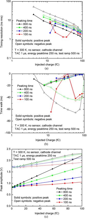
1594                                                                     IEEE TRANSACTIONS ON NUCLEAR SCIENCE, VOL. 55, NO. 3, JUNE 2008

                                                                    is about one third of      . We give details about this configura-
                                                                    tion elsewhere [25].
                                                                       For voltage amplifiers that must provide negative swing at the
                                                                    output, the capacitor        was introduced. For negative output
                                                                    swings, the voltage at the gain node (drain node of the load         )
                                                                    is slew-rate limited by the current in       . When this occurs, the
                                                                    input voltage of the amplifier suddenly increases, and the drain
                                                                    voltage of the current source         falls. The capacitor       uses
                                                                    this decrease to send additional current to the gain node, thereby
                                                                    improving the performance for large signals. A typical value of
                                                                         is about 1 pF.
                                                                       The output stage consists of a source follower                 as-
Fig. 2. Block diagram of the ASIC.                                  sisted by its scaled-down replica                 and by a differen-
                                                                    tial amplifier, generating a local feedback. The dc gate voltage
                                                                    of the source       is forced to the gate voltage of         . During
                                                                    transients, the gate voltage of        is dynamically adjusted, in-
                                                                    creasing or decreasing the drain current so that the loaded output
                                                                    voltage follows its unloaded replica. A fast negative signal ap-
                                                                    plied to the gate of       and       produces a differential signal
                                                                    at the input of the differential amplifier. As a consequence, the
                                                                    gate of       , which is connected to the output of the differential
                                                                    stage, moves in the positive direction. In this way the current
                                                                    in        is dynamically increased and it is not limited by the dc
Fig. 3. Block diagram of the anode channel.                         bias value. This increased current allows a faster discharging of
                                                                    the output node with respect to the case of a traditional source
                                                                    follower without local feedback. The circuit works also for pos-
the digital signals and supplies are at the top. The three large    itive input signals. In this case the transistor         starts to be
holes at the bottom of the interposer are for the connection of     switched off by the negative output of the differential stage. In
the cathode signal and for the bias of the anode-grid ( 100 V).     this way a larger fraction of the current flowing in        is sent to
The cathode’s bias circuitry, not shown, is placed close to the     the output. However, in this case, the advantage with respect to
cathode electrode. The interposer is connected to a mother          a simple source follower configuration is limited by the amount
board that assures a regulated supply and can accommodate           of the dc current flowing in          . In order to work properly,
nine interposers in a 3 3 configuration.                            the time constants of the output node and unloaded replica must
   Fig. 2 is a block diagram of the ASIC that comprises 124         be properly set through their current and scaling factor. Typical
channels (122 read-out negative charge, two read-out positive),     currents through the                , and differential stage are, re-
bias circuitry, six 10-bit DACs, two test-signal generators, one    spectively, about 20 A, 1 A, and 4 A. A typical source fol-
temperature sensor, configuration register, logic for configura-    lower scaling factor is 20. The network                , with typical
tion and readout, multiplexers, and analog monitors.                values of 10 k , 100 fF, provides compensation and bypasses
   Each of the 122 anode channels, shown in Fig. 3, imple-          the active loop at the highest frequencies.
ments a low-noise charge amplifier with single-stage-compen-           The charge amplifier is followed by a 5th order shaper with
sated adaptive continuous reset [23] having charge gain of 48.      complex conjugate poles, an adjustable peaking time (0.25 s,
The input MOSFET is a p-channel device optimized for 3 pF           0.5 s, 1 s, and 2 s), and an output baseline stabilized with
input capacitance [24], with gate size          0.36 m/300 m        a Baseline Holder (BLH) [26]. It follows a discriminator with
(technology is CMOS 0.25 m) and biased at a drain current of        4-bit trimmer, a peak and timing detector, and a Time-to-Ampli-
about 100 A, corresponding to 250 W dissipated in the input         tude Converter (TAC) (the duration of ramp is adjustable to 1 s,
branch. With a transconductance          1.7 mS and a gate capac-   2 s, 3 s, and 4 s). The amplitude of the pulse is measured and
itance        650 fF the input MOSFET contributes to the ENC        stored in an analog memory using a multi-phase peak-detection
with about 75 electrons rms at 3 pF input capacitance (assuming     configuration [27]. The TAC converts the timing of the anode
a high order shaper with 1 s peaking time).                         event into a voltage. The ramp starts at a trigger released by the
   The voltage amplifiers adopted in the charge amplifier and       peak detector at the time of the peak, and is stopped by an ex-
shaper stages implement some new configurations. These con-         ternal trigger common to all TACs [28]. Section III has details of
figurations, shown in Fig. 4, aim to improving the performance      this timing method. The channel includes a mask function and a
while maintaining the power dissipation within specifications.      test capacitor connected to a test-pulse generator, common to all
   The input MOSFET          is followed by a dual-cascode stage    channels, whose amplitude is controlled by a 10-bit DAC. The
            , which increases the amplifier’s dc gain and lowers    shaped pulse from it can be routed to an auxiliary analog output
the impedance at the drain node of      . The voltage drop across   (analog monitor). The entire channel is characterized by a gain
      has negligible impact in our charge amplifier’s configura-    of about 20 mV/fC (about 18 mV/fC at 0.25 s peaking time)
tions based on continuous reset. The typical gate width of          and dissipates about 1.35 mW.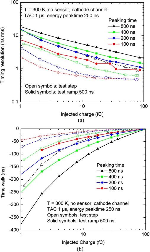
DE GERONIMO et al.: READOUT ASIC FOR 3D POSITION-SENSITIVE DETECTORS                                                                          1595

Fig. 4. Schematic of a voltage amplifier implementing some new configurations.

Fig. 5. Block diagram of the cathode channel.

   Fig. 5 shows the cathode channel, which implements a low-                     the second a 3rd order unipolar-shaping with complex con-
noise charge amplifier with dual stage adaptive reset having total               jugate poles and an adjustable peaking time (100 ns, 200 ns,
charge gain of 48. The input MOSFET is a p-channel device                        400 ns, and 800 ns), while the third provides a differentiation
optimized for 6 pF input capacitance, with gate size                             on the unipolar shaping, meaning a bipolar shaping (peaking
0.36 m/600 m and biased at a drain current of about 200 A,                       time about 50 ns, 100 ns, 200 ns, and 400 ns). The fourth
corresponding to 500 W dissipated in the input branch. With a                    output constitutes an inversion of the third output. These four
       3.4 mS and a         1.3 pF, it contributes to the ENC with               outputs measure the timing of the cathode’s signals via three
about 100 electrons rms at 6 pF input capacitance (assuming a                    different timing methods, discussed in detail in Section III. The
high order shaper with 1 s peaking time). The remainder of the                   timing circuits use discriminators with 4-bit trimmers, peak
channel splits in three sections providing, respectively, energy                 detectors and TACs (ramp durations adjustable to 1 s, 2 s,
measurement, timing measurement, and a preamplifier monitor                      3 s, and 4 s). The channel has a mask function and a test
(the latter not shown in Fig. 5).                                                capacitor connected to a pulse or ramp generator, common
   The cathode’s energy section implements a 5th order shaper                    to all channels, the amplitude of which is controlled by a
with complex conjugate poles and an adjustable peaking time                      10-bit DAC. Test ramps can be generated with adjustable
(0.25 s, 0.5 s, 1 s, and 2 s), a BLH, a discriminator with                       slope and duration, thus simulating actual cathode signals. For
4-bit trimmer, and a multi-phase peak detector. The cathode’s                    monitoring, the charge amplifier’s voltage output is available
timing section includes a multi-stage shaper with four outputs:                  through a dedicated output (preamplifier monitor). The shaped
the first provides a replica of the charge preamplifier’s output,                pulse from the energy and timing sections can be routed to the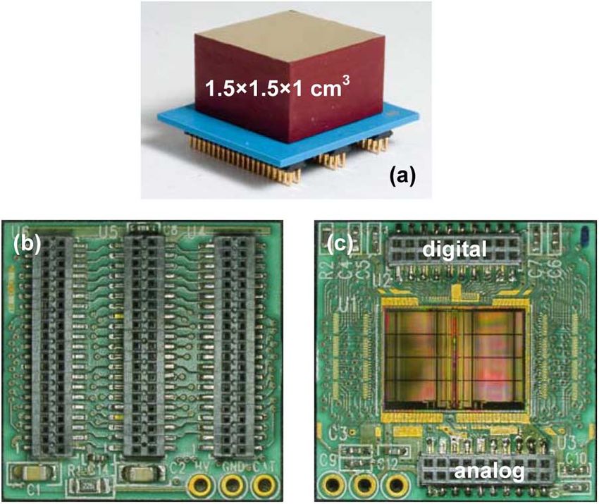
1596                                                                         IEEE TRANSACTIONS ON NUCLEAR SCIENCE, VOL. 55, NO. 3, JUNE 2008

auxiliary analog output (analog monitor). The whole channel             amplifier. Because the holes have poor transport properties, only
is characterized by a gain of about 20 mV/fC for the energy             the electrons effectively contribute to the currents, with the con-
section, and about 23 mV/fC and 15 mV/fC, respectively, for             sidered time constants.
the unipolar shaper and bipolar shaper in the timing section; it           The signal induced in the cathode, a planar electrode, starts
dissipates overall about 5.25 mW.                                       at the time of interaction and stops when the electrons reach the
   The ASIC operates in two sequent phases, acquisition and             anodes, to which the electrons travel at a speed that depends
readout, controlled by an external Low Voltage Differential             upon the applied voltage. Neglecting the holes, the duration of
Signal (LVDS) EN. The acquisition phase reads out and pro-              the induced signal depends on the applied voltage and depth
cesses the signals from the sensor; the readout phase makes             of interaction: it is longer when the interaction is in the prox-
the measurements available to the external electronics for              imity of the cathode (since the electrons travel through the whole
analog-to-digital conversion. In the former, EN high, all chan-         sensor), and declines to negligible values as the interaction oc-
nels become sensitive to input events. When an event occurs             curs closer to the anodes. Consequently, for a given energy, the
and a first peak is found, the ASIC releases a LVDS flag, FL,           total induced charge is higher when the interaction occurs close
and then the external electronics can stop acquisition by low-          to the cathode and decreases to negligible when the interaction
ering the EN. This signal is used as stop trigger for all TACs.         is closer to the anodes. The voltage signal at the output of the
Having entered the readout mode, all analog outputs (energy             charge amplifier, which is the integral of the induced current, is,
and timing) from all channels are made sequentially available,          to a first-order, a ramp with a slope proportional to the energy
with a LVDS clock CK, at two dedicated analog outputs.                  (i.e., to the total charge generated by the ionization) and dura-
   The ASIC discriminates events based only on anode signals.           tion proportional to the depth of interaction. For a given energy,
Once this is enabled (with EN high), should an anode signal ex-         the final amplitude of the ramp is proportional to the depth of
ceed the threshold, then the peak amplitude and timing measure-         interaction.
ments are enabled in all other anodes. The flag FL is released,            The signal induced in the anode is subject to the small-pixel
after a delay of 200 ns, at the time the first peak is found. The an-   effect [31]–[33]. Since it is distributed among all anodes and
odes process the amplitude and timing of the highest peak (the          anodes-grid, it remains negligible until the electrons approach
peak detector has a single analog memory) until the acquisition         the anodes at a distance of about one pixel pitch. Then a strong
stops (EN low). In one option, the timing can be measured only          current is induced in those anodes that collect the charge. The
from the first peak; this choice option can be valuable for ex-         hole-induced signal remains small for every single pixel, be-
tracting timing information from inductions occurring in those          cause the holes move slowly towards the cathode or are trapped.
pixels neighboring the ones above threshold. In another option,         Consequently, unlike the cathode, the total induced charge is, to
channels that did not exceed the threshold can be forced to store       a first order, independent of the depth of interaction and only
that amplitude at the time of the first above-threshold peak. This      depends on the event’s energy. The voltage signal at the output
one can be useful to force the sampling of negative amplitudes          of the charge amplifier is, to a first-order, a step with amplitude
that may result from induction in the pixels next to the ones           proportional to the energy, independent of the depth of the inter-
above threshold [29], [30].                                             action. Compared to planar electrodes, the small-pixel configu-
   A cathode signal exceeding the threshold is always processed         ration effectively makes the detector sensitive to only one kind
for peak amplitude and timing, but the event will not trigger the       of charges, the electrons.
flag FL. The cathode will continue processing the amplitude and            In the absence of electron trapping, and assuming an ideal
timing of the highest peak until the acquisition stops (EN low).        small-pixel effect, the total charge measured at the anode (or an-
   Except for the serial configuration signals, all the digital         odes) is proportional to the event’s energy. Taking electron trap-
inputs and outputs are LVDS. The ASIC includes one test-pulse           ping and second-order small-pixel effects into account, then the
generator for the anodes and one test pulse/ramp generator for          anode signals show a non-negligible dependence on the depth
the cathode, controlled by independent LVDS clock signals               of interaction that considerably affects spectral performance.
and two 10-bit DACs. The common thresholds are controlled                  This dependence can be compensated for by measuring, for
by four 10-bit DACs and a one 4-bit DAC. The temperature                each event, both the amplitude of the signal at the anode and the
sensor is characterized by a nominal response of 1.52 V                 depth of the interaction, and by applying to the amplitude the
5.67 mV/ C. The outputs from the DACs and temperature                   associated corrective coefficient. The depth of interaction can
sensor can be routed to the auxiliary analog output (analog             be extracted to a first order from the ratio between the ampli-
monitor). The whole ASIC dissipates 250 mW, with an effec-              tude of the cathode signal and the one of the anode (or sum of
tive power per channel of about 2 mW. Constructed in CMOS               anodes). This approach is effective for ionizing events having a
0.25 m, the die, measuring 11.3 mm                8.2 mm, has 208       single point of interaction or involving only a few anodes. For
input/output pads.                                                      events with multiple points of interaction or encompassing sev-
                                                                        eral anodes, the depth of each point can be more efficiently ex-
                     III. TIMING METHODS                                tracted from measuring the relative drift time associated with
   An ionizing event produces electron-hole pairs in CZT mate-          each anode signal, i.e., the delay from the time of interaction,
rial in an amount proportional to the energy of the event. Under        measured on the cathode signal, to the time the electrons reach
the applied voltage, the electrons and holes move, respectively,        each anode. All these bi-parametric approaches afford correc-
from the point of interaction to the anodes and cathode. The            tion coefficients for each volumetric pixel (voxel) in the sensor
currents induced in both are measured by the associated charge          [20]–[22], [32].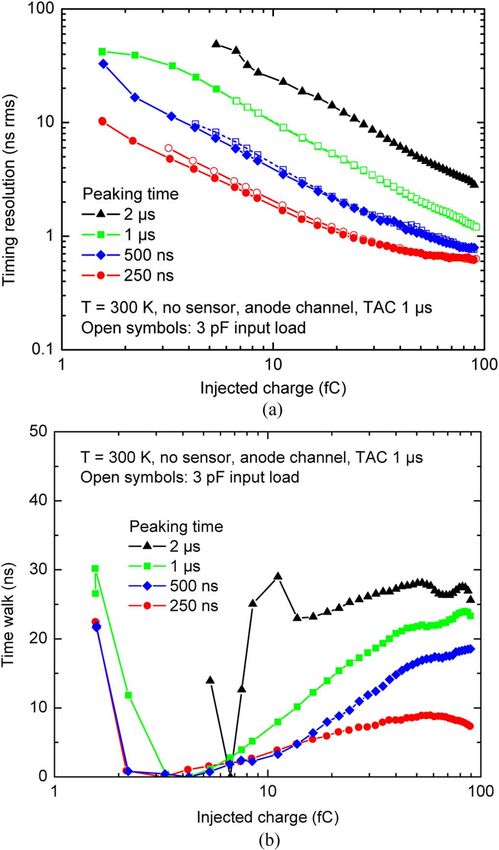
DE GERONIMO et al.: READOUT ASIC FOR 3D POSITION-SENSITIVE DETECTORS                                                                             1597

Fig. 6. Block diagram of the peak detector’s circuit.

   Techniques were implemented in the ASIC to accurately
measure the timing of the anode and cathode signals.
   The timing of the former is obtained, as anticipated in the
previous Section, by measuring the peaking time of the anode-
shaped pulse. In contrast to timing measured from the threshold          Fig. 7. Theoretical timing resolution from (1) assuming a unipolar shape with
crossing on unipolar pulses, this peaking-time method has the            peaking time of 1 s and energy resolution 300 electrons rms. The case of
advantage of being, to a first order, independent of the ampli-          threshold crossing, along with the associated time walk, also is shown.
tude. In principle, the timing of the peak-found signal of the
peak detector circuit [27], shown in Fig. 6, is equal to the one
of the zero-crossings on a bipolar pulse. The current flowing            threshold crossing on the same unipolar pulse is depicted, along
through the hold capacitor          during peak detection equals the     with the associated time walk, assuming a threshold at 0.5% of
derivative of the input pulse according to                         .     the maximum amplitude.
When the signal            approaches the peak, the current      ap-        The results in (1) and Fig. 7 assume there is a negligible
proaches zero, and the voltage, , equals                    . Imme-      contribution to the noise from the shaper, the peak detector,
diately after the peak, the signal, , starts falling and, due to the     the comparator, and the downstream stages. In practice, over-
high gain,       , of the differential amplifier the output voltage,     looking these other contributions (as we partially did) can se-
   , sharply increases towards             crossing the comparator       verely limit the timing resolution. Particular attention must be
threshold,         , set at a voltage                              ,     paid to the residual high-frequency noise components from the
where           is the threshold voltage of the controlled current       last stages of the shaper, and from the differential amplifier of
source      .                                                            the peak detector. The signal, , decreases with the peaking
   The timing resolution achievable with this method can be              time, and its slope                 declines with the square of the
approximated with [34]                                                   peaking time. On the other hand, these noise components, along
                                                                         with their emphasis by the derivative, are, to a first order, inde-
                                            ENC                          pendent of peaking time. The contribution to the timing reso-
                                                                         lution then is proportional to the square of the peaking time,
                         ENC                                             and can be approximated with                         , where         is
                                                                  (1)    the corresponding rms current noise. A resistor placed in se-
                                                                         ries with the capacitor         , to help stabilize the peak detector
where       is the noise on the current signal , and           is the    loop, also would filter part of such high-frequency noise. The
derivative calculated at the time,       , of the threshold crossing     noise from the comparator can be evaluated as                  , where
of the comparator, where                            then is the cur-          is the rms voltage noise at its input, and           is the slope
rent. We note that         is set by the threshold         , and, for    of      . The slope can be approximated from the Taylor series
      approaching the time          at which       peaks, it follows     of the signal,              , immediately after the peak, yielding
that                         . In (1), the noise      is assumed to                                                 where A is the difference
be dominated by that on the shaped pulse, , from the first               voltage gain. Again, this contribution, usually small, is propor-
front-end stage, and it is calculated in (1) as ENC multiplied           tional to the square of the peaking time. Assuming that the
by the gain from the signal charge Q to the current in          (i.e.,   timing signal is converted into a voltage using a TAC (as in
   /Q, where       is the peak value of ). Therefore, the term           our case), the series noise from the TAC and its readout can be
ENC is calculated assuming a bipolar shape (current ) with               approximated with sqrt                                        where S
peaking time      . Normalized coefficients can be adopted [34],                is the spectral noise power density of the current flowing
yielding the final expression in (1) that depends only on Q and          into a capacitor          to generate the ramp,          is the ramp’s
the peaking time of . For a 5th order shaper with complex                duration, and         is its slope. The contribution from the down-
conjugate poles, they are                          , and                 stream stages (e.g., the buffer, ADC) can be approximated with
[34]. Assuming a unipolar pulse with peaking time 1 s and                              where         is their rms input voltage noise.
resolution 200 e rms, the timing resolution from (1) can be                 For measuring the timing of the cathode signals, we estab-
plotted as done in Fig. 7. In the same figure, the resolution for        lished three different methods: preamplifier multi-threshold,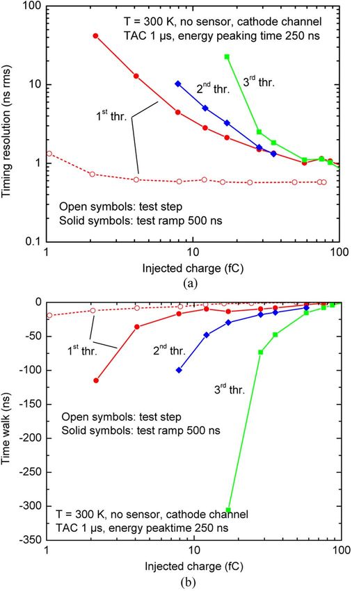
1598                                                                                     IEEE TRANSACTIONS ON NUCLEAR SCIENCE, VOL. 55, NO. 3, JUNE 2008

                                                                                    depth of interaction. For events with single point of interaction,
                                                                                    the delay from the positive to the negative peak affords a
                                                                                    first order value for the electron drift time (i.e., the depth of
                                                                                    interaction). The ASIC measures amplitude and timing of both
                                                                                    positive and negative pulses.
                                                                                       By directly measuring the drift time and energy without re-
                                                                                    quiring the information from the anodes, the first and the last
                                                                                    methods of cathode timing are expected to offer better overall
                                                                                    performance. All three were designed to provide a timing reso-
                                                                                    lution better than 20 ns for charges above 1 fC.

                                                                                        IV. FABRICATION AND FIRST EXPERIMENTAL RESULTS
Fig. 8. Diagram illustrating the bipolar peaking time method for measuring             We fabricated the first prototype of the ASIC, with a layout
the timing of cathode signals. Two cases are illustrated, differing in energy and   size of 11.3 mm 8.2 mm, in a commercial CMOS 0.25 m
depth.                                                                              technology. Fig. 9 is a picture of the die. The 122 anode channels
                                                                                    plus two cathode channels are symmetrically arranged with 62
                                                                                    inputs on the left, and 62 on the right. The bias and readout
unipolar threshold, and bipolar peaking time. All take into                         circuitry are in the center, the analog outputs at the bottom, and
account the cathode signal’s relatively long induction time.                        the digital interface at the top. The channels are, respectively,
   The preamplifier multi-threshold method is performed di-                         100 m 5 mm and 200 m 5 mm for the anode and cathode.
rectly on the output voltage of the charge amplifier (before                        The total transistor count is about 300 000.
the shaping). As discussed, the voltage signal at the output of                        The ASIC was assembled as shown in Fig. 1(b) and (c), and
the charge amplifier is, to a first order, a ramp whose slope                       was characterized without a sensor and, preliminarily, with a
is proportional to the energy, and duration to the depth of                         121-pixel CZT sensor of 20 20 5 mm . Fig. 10 plots the
interaction. By measuring the timing of the crossing of three                       response of the anode channel to a 70 fC input charge for four
different thresholds [35] the slope of the signal (i.e., the energy)                peaking -time values. The baseline is about 245 mV.
can be reconstructed, and also the timing at the departing point                       Fig. 11 shows the ENC measured on cathode and anode chan-
of the ramp (i.e., the time of interaction). This method still                      nels as function of the peaking time, including the cases without
requires energy information from the anodes for those signals                       a sensor, with the sensor unbiased and biased. The measure-
that cross only the first threshold. A drawback here is the poor                    ments were taken with a true rms voltmeter at the channel analog
noise filtering, limited to the one introduced by the parasitics in                 output, available through the monitor function. Spectral mea-
the charge amplifier. For slow signals, as in our case, the noise                   surements with a test pulse and no sensor show an increase in the
may easily dominate the signal.                                                     ENC of about 15%–20%, due to the noise from the peak detector
   The unipolar threshold method, frequently adopted by                             circuit. In a revised version, we will consider reducing this con-
designers, consists of measuring the timing at the threshold                        tribution, mainly by optimizing the size of some components.
crossing of a fast-shaped cathode signal. It necessitates having                    This increase becomes negligible with the sensor connected.
an additional fast shaper associated with the cathode channel.                         An integral linearity error below        0.3% was measured for
Since the time at the crossing of the threshold depends on                          output signal amplitudes up to 2.25 V (including the 250 mV
the pulse’s amplitude and induction time, this measurement                          baseline), which corresponds to an input charge of 100 fC. A
exhibits considerable dependence on the energy and depth                            channel-to-channel dispersion of 5.2 mV rms and 1.5% rms (2%
of interaction. Accordingly, it requires additional calibration                     rms at 0.25 s peaking time) were, respectively, measured on the
based on the energy information from the anodes.                                    baseline and gain.
   The bipolar peaking time method is based on measuring                               The timing response of the anode channels was character-
amplitude and peaking time of the cathode signal filtered by                        ized, with the test pulse, in terms of resolution and time walk.
a fast bipolar shaper; hence, an additional fast shaper must be                     Fig.12(a) shows the measured resolution as function of the
added to the cathode channel. Bipolar-shaped signals exhibit a                      injected charge for the four peaking times. Values below 700 ps
unipolar response each time the slope of the charge amplifier                       were measured at a peaking time of 250 ns for charges above
voltage signal (i.e., the ramp) changes. The amplitude of the                       30 fC, limited by the noise from the TAC and downstream
resulting unipolar pulse is proportional to the change in slope,                    stages. For low amplitudes, the resolution was considerably
and the timing is related only to the time of the change in                         worse than the theoretical value (1). Further analysis revealed
slope. If the peaking time is small compared to the induction                       that the increase is dominated by the noise from the shaper and
time, the shaped signal responds with a positive unipolar pulse                     peak detector. For example, we observed that the resolution in-
when the ramp departs from the baseline, and with a negative                        creases faster than the increase in peaking time (see Section III).
unipolar pulse at the end of the ramp (Fig. 8). The amplitude of                    Further confirmation comes from the additional measurements
the positive pulse is proportional to the slope, and it provides                    (open symbols) shown in Fig. 12(a), obtained by loading
a first-order measurement of the energy. The peaking time is                        the input of the channel with a 3 pF capacitor. Preceding a
associated with the time the slope changes providing, to a first                    factor-of-two increase in rms noise at the shaper’s output, only
order, a timing measurement independent of the energy and                           a negligible increase is observed in timing resolution (compare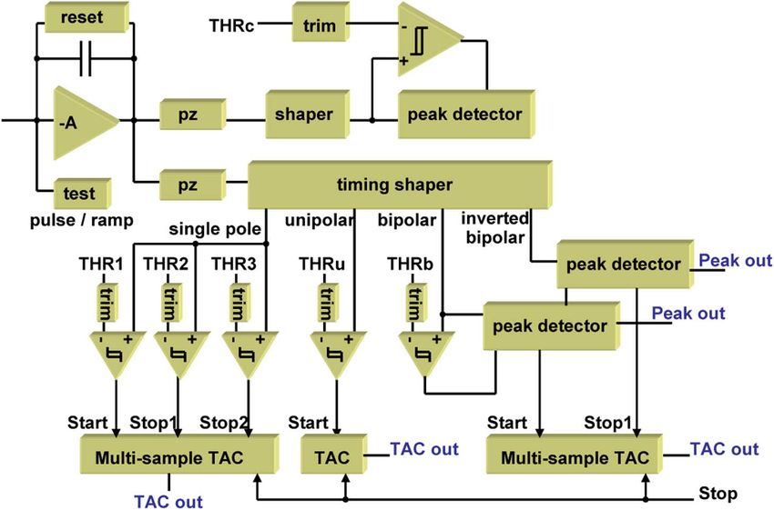
DE GERONIMO et al.: READOUT ASIC FOR 3D POSITION-SENSITIVE DETECTORS 1599
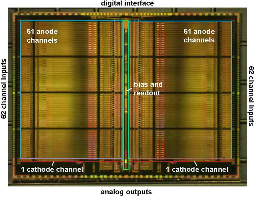
Fig. 9. Die photo, layout size 11.3 mm 2 8.2 mm.
Fig. 11. Measured ENC versus peaking time.
Fig. 10. Measured response to a 70 fC charge for the four peaking time values.
threshold, unipolar threshold, and bipolar peaking time. It was
accomplished via injecting charge with the integrated test pulse
the solid symbols to the open symbols), especially at longer and test ramp generators. The duration of the ramp was set to
peaking times. We have overlooked the impact of the noise 500 ns and the injected charge was altered by changing the
from the shaper and peak detector on the timing resolution; it ramp’s slope. The peaking time in the energy section of the
will be resolved in a later version, mainly by optimizing the cathode channel was set to 250 ns. The results from this char-
size of some components. acterization are reported here, while a comparative analysis will
Fig. 12(b) shows the measured time walk, referenced to the be published later.
minimum value, as function of the injected charge for the four For the preamplifier multi-threshold, Fig. 13(a) shows the
peaking times. The time walk is contained within 8 ns and 30 ns, measured resolution as function of the injected charge for the
respectively, at the shortest and longest peaking time. Almost four peaking times. The solid symbols correspond to the 500 ns
identical results were obtained with the 3 pF capacitor at the test ramp, while the open symbols represent the test pulse, for
input. which only the first threshold was characterized.
The timing response of the cathode channel was character- The first threshold was set at about 0.5 fC, while the second
ized using the three implemented methods: preamplifier multi- and third thresholds were set to cover as much as possible the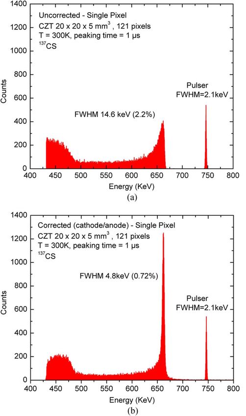
1600                                                                             IEEE TRANSACTIONS ON NUCLEAR SCIENCE, VOL. 55, NO. 3, JUNE 2008

                                                                            Fig. 13. Measured cathode timing resolution (a) and time walk (b) using the
Fig. 12. Measured anode- channel timing resolution (a) and time walk (b).   preamplifier multi-threshold method.

range of interest from 1 fC to 100 fC. We noted that, due to the            500 ns test ramp, and the open symbols to the test pulse. In
poor signal level, a minimum detectable charge of 2 fC, 8 fC, and           all cases, we measured a timing resolution below 20 ns. For
17 fC for the first, second, and third threshold, respectively, were        the ramp, the impact of the reduced speed of the signal on the
measured with the ramp. Excellent timing resolution was mea-                resolution is apparent. Fig. 14(b) shows the corresponding time
sured with the test pulse, while, in the most realistic case of the         walk referenced to the maximum value. Especially in the case
ramp, the timing resolution was below 20 ns for charges above               of the ramp, the time walk can be as high as 400 ns for low
3 fC. Fig. 13(b) shows the corresponding time walk referenced               charges.
to the maximum value, where, for the first threshold, values in                For the bipolar peaking time, Fig. 15(a) and (b) show the
excess of 100 ns were obtained for the test ramp. The difference            measured resolution of the test ramp as function of the injected
in timing between the thresholds, properly calibrated, provides             charge for the four peaking times. Due to a design error, for
a measure of the slope of the test ramp that allows for timewalk            a given charge the pulse amplitude was proportional to the
correction. To have a difference available, at least two thresh-            peaking time. This reduction in gain strongly affected the
olds must be crossed, which in Fig. 14 means having a charge                performance at low peaking times and will be corrected in a
above 8 fC. For signals from the sensor, this also constitutes              revision. Additionally, we saw considerable pick-up from the
a direct measurement of the ionized charge (i.e., the energy).              digital signals that prevented the characterization for charges
Suitable calibration can also provide the corrective coefficient            below 4 fC. Finally, as in the case of the anode, the noise from
for the time walk associated with the first threshold.                      the shaper and peak detector strongly affected these measure-
   For a unipolar threshold set at about 0.5 fC, Fig. 14(a) shows           ments, issues that also will be resolved later.
the measured resolution as function of the injected charge for                 As discussed in Section II, the amplitude of the pulse from
the four peaking times. The solid symbols correspond to the                 the peak detector, being proportional to the slope, is a measure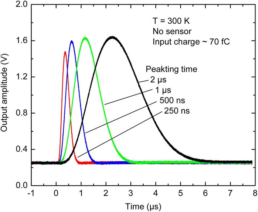
DE GERONIMO et al.: READOUT ASIC FOR 3D POSITION-SENSITIVE DETECTORS                                                                                1601

Fig. 14. Measured cathode timing resolution (a), and time walk (b), using the
unipolar method.

of the energy. A resolution between 300 and 500 rms electrons
was detected in the range of the four peaking times. Fig. 15(c)
shows the measured peak amplitude on the positive- and nega-
tive-peaks as function of the injected charge (i.e., as a function
of the slope).
   Fig. 16(a) plots a single pixel spectrum from a      Cs source
acquired at a peaking time of 1 s. Fig. 16(b) shows the cor-
rected spectrum using the cathode/anode ratio. The resolution
is about 4.8 keV (0.72 %) at 662 keV, while the contribution
from the electronics and leakage current is on the order of
2.1 keV.

              V. CONCLUSIONS AND FUTURE WORK
  We demonstrated that the performance of our first prototype
                                                                                Fig. 15. Measured cathode timing resolution (a), time walk (b), and peak
of an ASIC for 3D position-sensitive pixelated CZT sensors                      voltage (c) using the bipolar peaking time method.
shows good agreement with the design in its functionality and
energy resolution, where less than 200 electrons rms are mea-
sured with the sensor connected and biased. Margins for im-                     resolution below 20 ns can reasonably be expected from a revi-
provement were identified in the anode timing, where a final                    sion. Three different methods were characterized for resolving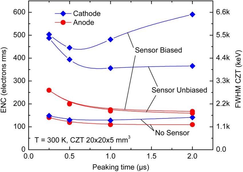
1602 IEEE TRANSACTIONS ON NUCLEAR SCIENCE, VOL. 55, NO. 3, JUNE 2008
[2] C. H. Malden and R. D. Speller, “A CdZnTe array for the detection
of explosives in baggage by energy-dispersive X-ray diffraction signa-
tures at multiple scatter angles,” Nucl. Instrum. Methods, vol. A449,
pp. 408–415, 2000.
[3] R. Arlt, J. Brutscher, R. Gunnink, V. Ivanov, K. Parnham, S. A. Soldner,
and J. Stein, “Use of CdZnTe detectors in hand-held and portable iso-
tope identifiers to detect illicit trafficking of nuclear material and ra-
dioactive sources,” in IEEE Nuclear Science Symp. (NSS) 2000 Conf.
Rec., 2001, pp. 4/18–4/23.
[4] T. H. Prettyman, K. D. Ianakiev, C. E. Moss, S. A. Soldner, M. R.
Sweet, and M. C. Browne, “Developments of high efficiency, multi-
element CdZnTe detectors for portable measurement applications,” J.
Radioanal. Nucl. Chem., vol. 248, pp. 295–300, May 2001.
[5] P. N. Luke, M. Amman, J. S. Lee, B. A. Ludewigt, and H. Yaver,
“CdZnTe coplanar grid detector array for environmental remediation,”
Nucl. Instrum. Methods, vol. A458, pp. 319–324, 2001.
[6] T. H. Prettyman, W. C. Feldman, K. R. Fuller, S. A. Storms, S. A.
Soldner, C. Szeles, F. P. Ameduri, D. J. Lawrence, M. C. Browne, and
C. E. Moss, “CdZnTe Gamma-ray spectrometer for orbital planetary
missions,” IEEE Trans. Nucl. Sci., vol. 49, no. 4, pp. 1881–1886, Aug.
2002.
[7] O. Limousin, “New trends in CdTe and CdZnTe detectors for X- and
gamma-ray applications,” Nucl. Instrum. Methods, vol. A504, pp.
24–37, 2003.
[8] W. Li, S. Li, S. Zhu, S. Yin, B. Zhao, G. Chen, S. Yin, H. Yuan, and H.
Xu, “Mercuric iodide single crystals for nuclear radiation detectors,”
IEEE Trans. Nucl. Sci., vol. 43, no. 3, pp. 1369–1371, Jun. 1996.
[9] L. J. Meng, Z. He, B. Alexander, and J. Sandoval, “Spectroscopic per-
formance of thick HgI2 detectors,” IEEE Trans. Nucl. Sci., vol. 53, no.
3, pp. 1706–1712, Jun.. 2006.
[10] Z. He and R. D. Vigil, “Investigation of pixelated HgI2 Gamma-ray
spectrometers,” Nucl. Instrum. Methods, vol. A492, pp. 387–401, 2002.
[11] R. Redus, M. Squillante, and J. Lund, “Electronics for high resolu-
tion spectroscopy with compound semiconductors,” Nucl. Instrum.
Methods, vol. A380, pp. 312–317, 1996.
[12] J. C. Lund, J. M. VanScyoc III, R. B. James, D. S. McGregor, and R.
W. Olsen, “Large volume room temperature gamma-ray spectrometers
from CdZnTe,” Nucl. Instrum. Methods, vol. A380, pp. 256–261, 1996.
[13] M. Amman and P. Luke, “Optimization criteria for coplanar-grid de-
tectors,” IEEE Trans. Nucl. Sci., vol. 46, no. 3, pp. 205–212, Jun. 1999.
[14] A. Burger, K. Chattopadhyay, H. Chen, X. Ma, J. O. Ndap, M. Schieber,
T. E. Schlesinger, H. W. Yao, J. Erickson, and R. B. James, “Defects,
in CZT crystals and their relationship to gamma-ray detector perfor-
mance,” Nucl. Instrum. Methods, vol. A448, pp. 586–590, 2000.
[15] F. Mathy, A. Gliere, E. G. d’Aillon, P. Masse, M. Picone, J. Tabary, and
L. Verger, “A three-dimensional model of CdZnTe gamma-ray detector
and its experimental validation,” IEEE Trans. Nucl. Sci., vol. 51, no. 5,
Fig. 16. Single pixel spectrum from a Cs source: (a) uncorrected, and pp. 2419–2426, Oct. 2004.
(b) corrected using the cathode/anode ratio. [16] E. G. d’Aillon, M. C. Gentet, G. Montemont, J. Rustique, and L.
Verger, “Simulation and experimental results on monolithic CdZnTe
gamma-ray detectors,” IEEE Trans. Nucl. Sci., vol. 52, no. 6, pp.
3096–3102, Dec. 2004.
cathode timing that will undergo further comparative analyses. [17] A. Shor, Y. Eisen, and I. Mardor, “Gamma spectroscopy with pixe-
Digital pick-up and low gain affect bipolar timing and will be lated CdZnTe detectors,” IEEE Trans. Nucl. Sci, vol. 51, no. 3, pp.
1204–1208, Jun. 2004.
resolved in a revision. Calibration routines also will be imple- [18] A. E. Bolotnikov, G. C. Camarda, G. W. Wright, and R. B. James,
mented using the integrated test pulse and test ramp. Finally, we “Factors limiting the performance of CdZnTe detectors,” IEEE Trans.
will undertake extensive characterization with pixelated CZT Nucl. Sci., vol. 52, no. 3, pp. 589–598, Jun. 2005.
[19] D. S. Bale and C. Szeles, “Design of high-performance CdZnTe quasi-
sensors. hemispherical Gamma-ray CAPture plus detectors,” Proc. SPIE, vol.
6319, 63190B, 2006.
[20] Z. He, W. Li, G. F. Knoll, D. K. Wehe, J. Berry, and C. M. Stahle, “3-D
ACKNOWLEDGMENT position sensitive CdZnTe gamma-ray spectrometers,” Nucl. Instrum.
Methods, vol. A422, pp. 173–178, 1999.
The authors are grateful to F. Ferraro, from eV Products, Div. [21] W. Li, Z. He, G. F. Knoll, D. K. Wehe, and Y. F. Du, “A modeling
of II-VI Inc., and Dr. A. Janos, from DNDO-DHS, for their en- method to calibrate the interaction depth in 3-D position sensitive
couragement and support. A special acknowledgment goes to CdZnTe gamma-ray spectrometers,” IEEE Trans. Nucl. Sci., vol. 47,
no. 3, pp. 890–894, Jun. 2000.
A. D. Woodhead for assistance with editing. This project was [22] F. Zhang, Z. He, and D. Xu, “Improved resolution for 3-D position
founded by the Domestic Nuclear Detection Office (DNDO) of sensitive CdZnTe spectrometers,” IEEE Trans. Nucl. Sci., vol. 51, no.
the US Department of Homeland Security. 5, pp. 2427–2431, Oct. 2004.
[23] G. D. Geronimo, P. O’Connor, and J. Grosholz;, “A generation of
CMOS readout ASICs for CZT detectors,” IEEE Trans. Nucl. Sci., vol.
REFERENCES 47, no. 6, pp. 1857–1867, Dec. 2000.
[24] G. D. Geronimo and P. O’Connor, “MOSFET optimization in deep
[1] A. Owens and A. Peacock, “Compound semiconductor radiation de- submicron technology for charge amplifiers,” IEEE Trans. Nucl. Sci.,
tectors,” Nucl. Instrum. Methods, vol. A531, pp. 18–37, 2004. vol. 52, no. 6, pp. 3223–3232, Dec. 2005.DE GERONIMO et al.: READOUT ASIC FOR 3D POSITION-SENSITIVE DETECTORS 1603
[25] G. D. Geronimo, J. Fried, E. Frost, B. F. Phlips, E. Vernon, and E. A. [31] H. H. Barret, J. D. Eskin, and H. B. Barber, “Charge transport in arrays
Wulf, “Front-end ASIC for a silicon compton telescope,” presented at of semiconductor gamma-ray detectors,” Phys. Rev. Lett., vol. 75, pp.
the 2007 IEEE Nucl. Sci. Symp., Honolulu, HI, Oct. 2007. 156–159, July 1995.
[26] G. D. Geronimo, P. O’Connor, and J. Grosholz, “A CMOS baseline [32] E. G. d’Aillon, M. C. Gentet, G. Montemont, J. Rustique, and L.
holder (BLH) for readout ASICs,” IEEE Trans. Nucl. Sci., vol. 47, no. Verger, “Simulation and experimental results on monolithic CdZnTe
3, pp. 818–822, Jun. 2000. gamma-ray detectors,” IEEE Trans. Nucl. Sci., vol. 52, no. 6, pp.
[27] G. D. Geronimo, P. O’Connor, and A. Kandasamy, “Analog CMOS 3096–3102, Dec. 2005.
peak detect and hold circuits, Parts 1 and 2,” Nucl. Instrum. Methods, [33] U. Lachish, “Driving spectral resolution to the noise limit in semicon-
vol. A484, pp. 533–556, 2002. ductor gamma detector arrays,” IEEE Trans. Nucl. Sci., vol. 48, no. 3,
[28] A. Dragone, G. D. Geronimo, J. Fried, A. Kandasamy, P. O’Connor, pp. 520–523, Jun. 2001.
and E. Vernon, “The PDD ASIC: Highly efficient energy and timing [34] G. De Geronimo, , K. Iniewski, Ed., “Low-noise electronics for ra-
extraction for high-rate applications,” in 2005 IEEE Nucl. Sci. Symp. diation sensors,” in Circuits for Emerging TechnologiesK. Iniewski,
Conf. Rec., 2006, vol. 2, pp. 914–918. Ed. Boca Raton, FL: CRC Press, to be published.
[29] S. E. Anderson, B. Donmez, and Z. He, “Sub-pixel position resolution [35] A. R. Frolov, T. V. Oslopova, and Y. N. Pestov, “Double threshold
in pixelated semiconductor detectors,” in 2007 IEEE Nucl. Sci. Symp. discriminator for timing measurements,” Nucl. Instrum. Methods, vol.
Conf. Rec., 2007, vol. 2, pp. 1569–1576. A356, pp. 447–451, 1995.
[30] H. Krawczynski, I. Jung, A. Burger, and M. Groza, Thick CZT [36] R. Redus, M. Squillante, and J. Lund, “Electronics for high resolu-
Detectors for Space-Borne x-Ray Astronomy [Online]. Available: tion spectroscopy with compound semiconductors,” Nucl. Instrum.
arXiv:astro-ph/0410077 2004 Methods, vol. A380, pp. 312–317, 1996.You can also read