A 38 DBI GAIN, LOW-LOSS, FLAT ARRAY ANTENNA FOR 320 GHZ TO 400 GHZ ENABLED BY SILICON-ON-INSULATOR MICROMACHINING - DIVA
←
→
Page content transcription
If your browser does not render page correctly, please read the page content below
IEEE TRANSACTIONS ON ANTENNAS AND PROPAGATION                                                                                                  1

        A 38 dBi Gain, Low-Loss, Flat Array Antenna
            for 320 GHz to 400 GHz Enabled by
            Silicon-On-Insulator Micromachining
   Adrian Gomez-Torrent, Graduate Student Member, IEEE, Takashi Tomura, Member, IEEE, Wataru Kuramoto,
 Jiro Hirokawa, Fellow, IEEE, Issei Watanabe, Akifumi Kasamatsu, Joachim Oberhammer, Senior Member, IEEE

   Abstract—Two high-gain flat array antenna designs operating                  reason, the interest in developing high gain and broadband
in the 320 – 400 GHz frequency range are reported in this paper.                antennas at frequencies above 300 GHz has increased in the
The two antennas show measured gains of 32.8 dBi and 38 dBi                     last years [4]–[10].
and consist of a 16 × 16 (256) element array and a 32 × 32 (1024)
element array, respectively, which are fed by a corporate H-tree                   One of the main difficulties when implementing antenna
beamforming network. The measured operation bandwidth for                       frontends in the sub-millimeter wave (sub-mmW) range and
both antennas is 80 GHz (22 % fractional bandwidth), and the                    above is the reduced size of the wavelength, that scales all
total measured efficiency is above −2.5 dB and above −3.5 dB for                components down in size. Optical systems such as reflectors
the two designs in the whole bandwidth. The low measured loss                   or lenses, which are several wavelengths in size and do not
and large bandwidth are enabled by optimizing the designs to
the process requirements of the SOI micromachining technology                   usually require micrometer size features, are relatively easy to
used in this work. The total height of the antennas is 1.1 mm (1.2              manufacture up to the THz range [4], [5]. Reflectarrays can
λ at the center frequency), with sizes of 15 mm × 18 mm and                     be a good alternative to reflectors and can be manufactured by
27 mm × 30 mm for both arrays. The antennas are designed to                     a lithography process at a low cost [10]; however, they have
be directly mounted onto a standard WM-570 waveguide flange.                    a narrow operation bandwidth and usually have low radiation
The design, fabrication, and measurements of eight prototypes
are discussed in this paper and the performance of the antennas                 efficiency.
compared to the simulated data, as well as manufacturability                       These optical systems can achieve high gain values and
and fabrication repeatability are reported in detail.                           wideband operation, but they tend to be heavy, bulky, and
  Index Terms—corporate beamforming network, array anten-                       involve careful alignment of the feed antenna. Quasi-optical
nas, waveguide arrays, terahertz radiation, submillimeter-wave                  systems have been developed as an alternative solution to opti-
antennas, silicon micromachining, silicon on insulator                          cal systems [6], [7], [11]. They can integrate one-dimensional
                                                                                reflectors or lenses in parallel plate waveguide (PPW) technol-
                          I. I NTRODUCTION                                      ogy, thus reducing the total volume and mass of the system,
                                                                                but limiting the beamforming to one plane. Therefore, quasi-

W        IRELESS mobile traffic keeps growing, and it is
         expected to reach 131 EB/month by 2024 [1]. The
current trend to meet this traffic demand is to make use of
                                                                                optical systems need an additional beamforming network
                                                                                (BFN) in PPW technology to generate a pencil-shaped beam
                                                                                [11], making their fabrication still challenging in the THz
the available terahertz (THz) region of the electromagnetic                     range.
spectrum that will enable multi-Gbps wireless data links                           Corporate-feed array antennas can provide high gain and
[2]. One of the main problems with THz links is the high                        broadband operation, but they require waveguide BFNs with
atmospheric attenuation, which degrades the signal-to-noise                     increasing complexity as the number of elements of the array
ratio and, thus, the maximum capacity of the channel.                           increases. The geometrical complexity of the BFNs makes
   The gain and bandwidth of the antennas used for data links                   their fabrication extremely challenging at THz frequencies
are critical parameters in order to increase the channel capacity               by classic CNC-milling techniques, due to the small features
[2], [3], which is particularly relevant in the THz range due to                and high uniformity required to achieve a good performance.
the higher atmospheric attenuation mentioned above. For this                    Tekkouk et al. [8] reported on the first corporate feed ar-
  A. Gomez-Torrent and J. Oberhammer are with the Division of Micro and         ray antenna above 300 GHz using silicon micromachining of
Nanosystems, School of Electrical Engineering and Computer Science, KTH         standard silicon wafers. Although this approach allowed the
Royal Institute of Technology, Stockholm SE-100 44, Sweden                      first implementation of such an antenna, the design failed to
  T. Tomura, W. Kuramoto, and J. Hirokawa are with the Department of
Electrical and Electronic Engineering, Tokyo Institute of Technology, Tokyo     take full advantage of the silicon micromachining technology,
152-8552, Japan                                                                 which resulted in increased loss and narrow bandwidth. The
  I. Watanabe and A. Kasamatsu are with the National Institute of Information   results served as a proof of concept for the use of sili-
and Communications Technology, Tokyo 184-8795, Japan
  The contribution by KTH to this work has received funding from the            con micromachining for sub-mmW array antennas, but also
European Research Council (ERC) under the European Union’s Horizon              brought out the importance of a fabrication-oriented design
2020 research and innovation programme (grant agreement No 616846), and         for waveguide components when approaching the THz range.
the Swedish Foundation for Strategic Research Synergy Grant Electronics
SE13-007. This work is supported in part by JSPS Grand-in-Aid for Science          Silicon micromachining is a promising alternative to classi-
Research (17H01278).                                                            cal machining techniques for the implementation of waveguide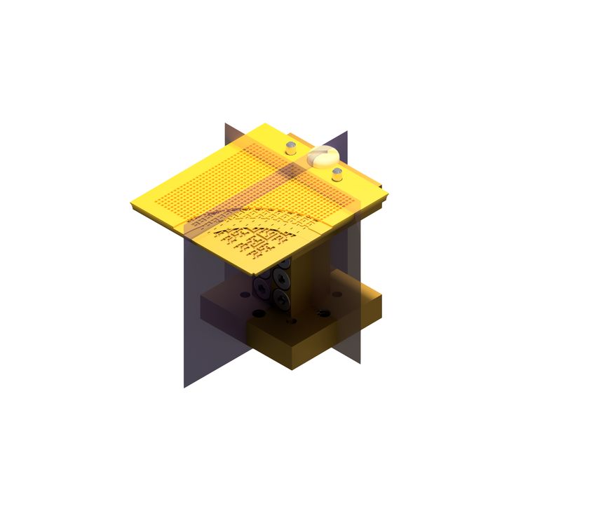
IEEE TRANSACTIONS ON ANTENNAS AND PROPAGATION 2
components in the sub-THz frequency range. Silicon micro-
machining can be used to fabricate low-loss waveguides [12], Alignment pins
high quality factor filters [13], complex waveguide 3D geome- Nylon screw
tries such as turnstile orthomode transducers [14], switches 30 mm
and phase shifters [15]–[17], or antennas [5], [11], [18]. The
1.1 mm
authors have also recently demonstrated the integration of
monolithic microwave integrated circuits (MMICs) in a silicon
micromachined platform where the RF, IF, and DC networks zy
are homogeneously integrated [19]. x
26 mm
This work presents two high gain array antennas in the
320 – 400 GHz frequency range in silicon on insulator (SOI)
micromachining technology. The SOI technology allows for Radiating elements
multistep complex waveguide geometries [14], enabling a new Power dividers
design of the input transition, BFN, and radiation cell in [8] to BFN
improve the bandwidth and drastically increase the radiation
efficiency. As a result, the 16 × 16 element array antenna B
presented here has double the bandwidth and a 5 dB loss
A
reduction as compared to previous work. These significant
improvements also enabled the development of a 32 × 32
element array, which represents the highest gain antenna in
the sub-THz frequency range not based on optical systems,
to the authors’ knowledge. The antennas in this work can be
directly mounted on a waveguide flange, avoiding the use of
additional CNC-milled test fixtures or custom-made flanges
that would increase the complexity, cost, and power loss of
the frontend.
II. A NTENNA S TRUCTURE AND D ESIGN
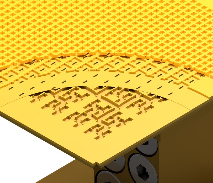
The antenna structure, mounted on a standard test port, is
shown in Fig. 1, and the cross-sections of the cutting planes
A and B are shown in Fig. 2. The antenna design consists
of 1) a 2n × 2n element array, 2) a corporate BFN, and 3) a
Fig. 1. CAD model of the 32 × 32 element array mounted on a standard
standard waveguide flange interface, which are implemented WM-570 waveguide piece.
in a four micromachined chip stack. All the electromagnetic
simulations for the design of the antenna were carried out
using the commercial software CST Studio Suite, and the
305�m
����m
A Chip 4
Chip 3
radiation cell was designed by a combination of the Method 305�m z Chip 2
of Moments and a numerical optimization genetic algorithm 305�m y Chip 1
[20], [21]. WM-570
The interface in chip 1 allows for a direct connection to (a)
a standard UG-387 flange, that is aligned by using a tightly-
fit circular hole and an elliptical hole in order to achieve a B
repeatable flange-to-chip connection [22]. The stepped E-plane
bend (see Fig. 3a) matches the standard WM-570 waveguide z
(570 µm × 285 µm) to the waveguide dimensions in the BFN x
(600 µm × 275 µm). The SOI wafer defines the height of Flange connection
Beamforming network
Power dividers
the waveguide and it is chosen to be as close as possible to Radiating elements
the standard waveguide height; the width of the waveguide is (b)
narrow enough to avoid the excitation of higher-order T En0 Fig. 2. Cross-sections of the antenna model in Fig. 1 shows: a) input wave-
modes, but it is made as wide as possible to reduce the guide and stepped E-plane bend, and b) beamforming network, power dividers,
insertion loss of the BFN. The height and length of the step and radiating elements. Dashed lines represent the different layers etched in
an SOI wafer. The underetch produced by the silicon micromachining process
are optimized to minimize the input reflections using the Trust is also represented and was considered during the design. Not to scale.
Region Framework algorithm implemented in CST [23], which
converges after seven iterations to a reflection level better than
−30 dB (see Fig. 4) by setting the initial parameters to half the designed to have reflections better than −20 dB in the operation
total height of the waveguide. bandwidth, as shown in Fig. 4. The final dimensions of the
The BFN consists of an in-plane H-tree network that feeds power divider are summarized in Fig. 3b. The complete power
2n−2 radiation cells. The H-plane power divider was first distribution network, shown in Fig. 5, was initially simulated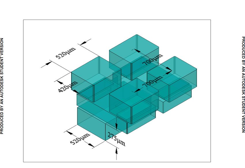
IEEE TRANSACTIONS ON ANTENNAS AND PROPAGATION                                                                                                                          3

                                                ����m                   ���m

                                          ����m                          ����m

                                                        ���m

                                                                                                                22mm
                                                                         ����m

                                                                          ����m

                    (a)                                        (b)
                          Radiating element                          132�m

                                                                                                                                     22mm
                                                520

                                                                530�m            ����m 1.04mm   Fig. 5. Design layout of the H-tree BFN for the 32 × 32 (n = 5) antenna.

   BFN feed
                                                                                                                                TABLE I
                                Power divider                                                                           SOI WAFER SPECIFICATIONS
                                                                        163�m

                                                               1.28mm                                           Handle layer    Device layer    Buried oxide layer
                                                                                                                 thickness       thickness       thickness (BOX)
                    (c)                                        (d)
                                                                                                       W1       275 ± 10 µm     30 ± 0.5 µm         3 µm ± 5 %
Fig. 3. Detailed geometry of the different sub-components in the antenna                               W2       320 ± 15 µm      180 ± 2 µm         1 µm ± 5 %
frontend: (a) input E-plane bend, (b) power divider, (c) perspective view of                           ∗
the radiation cell, and (d) top view of the radiation cell with different cavities                         Tolerances provided by the manufacturer, Utrasil LLC
in solid lines and coupling slots in dashed lines.

                                                                                                containing waveguides have a thickness of 275 µm, and the
                                                                                                power divider layer in chip 3 has a thickness of 180 µm.
                                                                                                The steps for impedance matching in chips 1 and 2 have
                                                                                                thicknesses of 144 µm and 162 µm, respectively. These mul-
                                                                                                tiple layer thicknesses were chosen to provide the best RF
                                                                                                performance, and are enabled by the SOI micromachining
                                                                                                technology, at a low fabrication complexity. A 3◦ sidewall
                                                                                                angle was included in all the simulations in order to consider
                                                                                                the effects of the etching process. This value is a good initial
                                                                                                approximation, but the actual underetch strongly depends on
                                                                                                the mask design, and small deviations can have some influence
                                                                                                in the input reflections of the antenna.
                                                                                                   Finally, the complete antenna structure, including the flange,
                                                                                                the alignment pins, and the nylon screw was simulated using
Fig. 4. Simulated input reflections for the different sub-components in the
antenna frontend: E-plane bend, power divider, and 2 × 2 radiation cell. The                    the Transient solver in CST to verify the overall performance.
shaded gray area marks the design bandwidth.
                                                                                                                           III. FABRICATION
and finely tuned in CST Schematic. For this simulation, each                                       Prototypes of two antenna designs were fabricated simulta-
of the 2n−2 outputs of the BFN was loaded with the simulated                                    neously: a 16 × 16 (n = 4) element array antenna, and a 32
S11 of the 2 × 2 element radiation cell, also plotted in                                        × 32 (n = 5) element array antenna with expected directivity
Fig. 4. The S-parameters of the complete antenna were then                                      values in the central frequency (f = 360 GHz) from full-
confirmed with a full-wave simulation of the whole structure.                                   wave simulations of 33.5 dBi and 39.5 dBi respectively. Two
   The radiation cell (see Fig. 2b and 3c,d) is fed through                                     fabrication runs were carried out, producing a total number
a coupling slot from the power distribution network. The                                        of six 16 × 16 element antenna prototypes and two 32 × 32
coupling slot in chip 2 feeds a cavity in chip 3 that acts as                                   element antenna prototypes.
a power divider by uniformly exciting a set of four slots in                                       The antennas are fabricated by deep reactive ion etching
chip 4. These slots in chip 4 couple the energy to the open                                     (DRIE) of SOI wafers at KTH Electrumlab, Stockholm, Swe-
ended waveguides, i.e., the radiating elements. This radiation                                  den. DRIE is based on the Bosch process, which alternates
cell, which is implemented by using only three chips, has a                                     silicon etching and passivation cycles in order to achieve large
total number of five layers of different thicknesses doubling                                   aspect ratio trenches on the wafer. The etching is performed in
the operation bandwidth as compared to [8].                                                     an STS plasma etching tool with an etch rate of 2.5 µm/min
   The coupling slots in the radiation cell have a thickness                                    and a selectivity over silicon oxide of 450:1. An end-point
            λ
of 30 µm ( 25  at the center frequency, 360 GHz), the layers                                    detection system, based on optical emission spectroscopy, is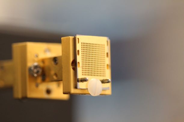
IEEE TRANSACTIONS ON ANTENNAS AND PROPAGATION                                                                                                             4

                              1.75 �m
Mask 2: PECVD oxide

                              2 �m
Mask 1: thermal oxide

SOI wafer                            1 �m

                                                                                                          20 mm
                        (a)                            (b)

                                                                                                                   (a)

                                                                                                       20 mm
                                            (c)

                                                                                                                   (b)

                                                                              Fig. 7. Pictures of the manufactured antennas mounted on a standard WM-
                                                                              570 waveguide flange. The antennas are aligned using two standard alignment
                                                                              pins and fixated with a nylon screw. The antenna in (a) is the 16 × 16 element
                                                                              array and the antenna in (b) is the 32 × 32 element array. The standard flange
                                                                              size is 20 mm × 20 mm.

                                                                              cross-section image of the silicon oxide hard mask stack is
                                                                              shown in Fig. 6a. This stack of hard masks is later used for
                                                                              the multi-step etching of the handle layer in W1 that forms
                                                                              the impedance matching steps. The manufactured stepped
                                                                              impedance transformer in chip 1, the H-tree BFN in chip 2,
                                            (d)                               and the radiating elements in chip 4 are shown in Fig. 6.
                                                                                 To form chip 3, see Fig. 2a, the device layer of W2 is etched
Fig. 6. SEM images of the manufactured devices: (a) hard mask stack
before DRIE process, (b) input waveguide section with stepped impedance       by using an oxide hard mask. The use of the device layer of
transformer in chip 1, (c) H-tree BFN in chip 2 showing waveguide structure   an SOI wafer is preferred over a standard silicon wafer due
and coupling slots, and (c) radiating elements with a zoomed view showing     to their better thickness tolerances, and due to the difficulty
the coupling slots.
                                                                              to produce and handle silicon wafers with thicknesses below
                                                                              200 µm. The handle layer of the SOI wafer has to be removed
used in the plasma chamber to detect when the BOX layer                       to release the etched structures, which is done by bulk dry
of the SOI wafer is exposed to the plasma. The biasing RF                     etching in a fluorine plasma (SF6 ). The BOX layer and oxide
power to the substrate is then switched to a pulsed mode, thus                mask in the device layer are finally removed by wet etching
avoiding any notching effects on the bottom of the trenches.                  in a 50 % hydrofluoric acid (HF) aqueous solution.
Two wafers (W1 and W2) are processed with a total number of                      After dry etching, the chips are cleaned in oxygen plasma
four photolithography masks. The specifications of both SOI                   and metalized with an adhesion layer of titanium/tungsten
wafers are shown in Table I.                                                  followed by 2 µm of gold in a DC magnetron sputtering tool.
  The multi-step SOI etching process described in [14] is                     Each antenna is then assembled by aligning the four chip
used to process W1. A scanning electron microscope (SEM)                      stack under the microscope, with the aid of integrated Vernier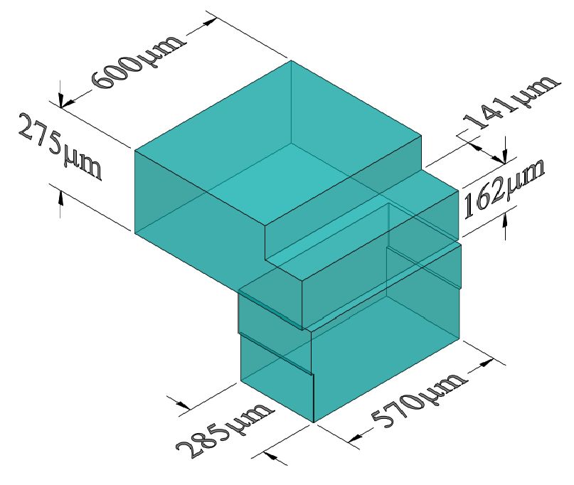
IEEE TRANSACTIONS ON ANTENNAS AND PROPAGATION                                                                                                            5

Fig. 8. Measured and simulated reflections for the 16 × 16 element array. The   Fig. 9. Measured and simulated reflections for the two prototypes of the 32
dashed black line shows simulated data, the solid blue line and shaded blue     × 32 element array.
area show the mean value and the standard deviation (±σ) of the measured
reflections for the six antenna prototypes.

scales, and thermal compression bonded at 200◦ C for 1 hour.
The authors described the bonding alignment method used in
this work in recent publications [11], [14], where better than
5 µm alignment accuracy is shown in the microscope images
of the Vernier scales. Fig. 7 shows the manufactured antennas
mounted in a standard waveguide flange.

                   IV. M EASUREMENT R ESULTS
   The gain, half power beamwidth (HPBW), input reflections,                               3.7°
and cardinal plane cuts of the radiation diagram were measured
for all the fabricated antennas. The data obtained from the six
16 × 16 element antennas is used to evaluate the new design
and fabrication technique by comparing it to the results in [8].
At the same time, the variability between different antennas is
investigated to evaluate the repeatability and uniformity of the                Fig. 10. SEM image of the cross-section of a waveguide showing the sidewall
SOI micromachining process. Finally, the measurement data                       profile angle.
of the two 32 × 32 element antennas is shown and com-
pared to the simulation results demonstrating the feasibility of
low-profile and high-gain antennas operating in the sub-THz                     of the impedance matching steps, or chip-to-flange alignment
frequency range.                                                                accuracy, since these would be random errors that cannot
   The input reflections are first measured using a Rohde &                     systematically affect all the devices in the same way. One of
Schwarz ZVA-24 VNA and a Virginia Diodes Inc. (VDI)                             the possible reasons is a deviation in the sidewall profile from
frequency extender with WM-570 waveguide flange interface.                      the 3◦ angle considered during the design. The actual sidewall
The measured RL of the 16 × 16 element antennas is in good                      angle in the antennas was found to be 3.7◦ , measured by a
agreement with the simulated data. Although the reflections                     destructive test of one of the chips in an SEM, as shown in
go above 10 dB around 340 GHz, the average value remains                        Fig. 10. This value can now be used for a fine optimization
below 16 dB in the design bandwidth. The RL is repeatable                       of the structure in a following fabrication iteration.
for all six antennas, as shown in Fig. 8, where the simulated                      The gain, HPBW, and radiation patterns of the antennas
value is plotted in dashed black lines, the mean value of the                   were measured in the millimeter-wave anechoic chamber at
measured data for all antennas in solid blue lines, and the                     NICT, Tokyo. The setup consists of a 2-axis azimuth/elevation
shaded area represents the standard deviation (±σ).                             stage with the antenna under test (AUT) in the origin of
   The input reflections of the two 32 × 32 element antennas                    rotation. A diagonal horn from VDI is used as the transmitting
are plotted in solid blue and red lines in Fig. 9. The measured                 antenna, and it is placed at a distance of 1.2 m from the AUT
data is also in good agreement with the simulations, and it                     in a direct illumination configuration. Two VDI frequency
is possible to observe the higher reflections around 340 GHz                    extenders driven by a Keysight PNA are used to measured
for this antenna design as well. This repeatable deviation                      the received power while scanning the AUT. A picture of the
from the expected results indicates that a fabrication error                    setup is shown in Fig. 11.
affects all antennas equally, hence ruling out misalignment                        The E-plane and H-plane cuts of the radiation diagram
errors between the different chips, deviations in the height                    were measured at three frequency points (325 GHz, 360 GHz,
IEEE TRANSACTIONS ON ANTENNAS AND PROPAGATION 6
E-plane f=325GHz E-plane f=360GHz E-plane f=400GHz
0 0 0
-10 -10 -10
-20 -20 -20
-30 -30 -30
el -40 -40 -40
-10 -5 0 5 10 -10 -5 0 5 10 -10 -5 0 5 10
Azimuth (deg) Azimuth (deg) Azimuth (deg)
z az
H-plane f=325GHz H-plane f=360GHz H-plane f=400GHz
0 0 0
-10 -10 -10
-20 -20 -20
Fig. 11. Radiation pattern measurement setup at NICT with 2-axis az/el -30 -30 -30
rotation stage.
-40 -40 -40
-10 -5 0 5 10 -10 -5 0 5 10 -10 -5 0 5 10
E-plane f=325GHz E-plane f=360GHz E-plane f=400GHz
Elevation (deg) Elevation (deg) Elevation (deg)
0 0 0
-10 -10 -10 Fig. 13. Measured and simulated radiation pattern for the 32 × 32 element
array. Dashed lines show the simulated data and the solid overlaid lines show
-20 -20 -20
the measured data of the two manufactured prototypes.
-30 -30 -30
-40 -40 -40
-10 -5 0 5 10 -10 -5 0 5 10 -10 -5 0 5 10
Azimuth (deg) Azimuth (deg) Azimuth (deg) 16 x 16 element array
H-plane f=325GHz H-plane f=360GHz H-plane f=400GHz
0 0 0
-10 -10 -10
-20 -20 -20
-30 -30 -30
32 x 32 element array
-40 -40 -40
-10 -5 0 5 10 -10 -5 0 5 10 -10 -5 0 5 10
Elevation (deg) Elevation (deg) Elevation (deg)
Fig. 12. Measured and simulated radiation pattern for the 16 × 16 element
array. Dashed lines show the simulated data, and the solid overlaid lines show
the measured data of the six manufactured prototypes. Fig. 14. Measured and simulated HPBW of all the manufactured antennas.
E-plane is shown in red, and H-plane is shown in blue. Dashed lines represent
the simulated data, and the discrete points are the measured values for each
antenna.
and 400 GHz). The radiation patterns of the six 16 × 16
element antennas in Fig. 12 show the excellent agreement of -5
f=325GHz
-5
f=360GHz
-5
f=400GHz
all the measurements with the simulated results. Black dashed
Elev. (deg)
Elev. (deg)
Elev. (deg)
lines show the simulated data, while the measurement data
0 0 0
is represented as solid grey lines. The measurement data of
the six prototypes has been condensed to one plot for space
5 5 5
reasons, showing the low variability in the measured results -5 0 5 -5 0 5 -5 0 5
Az. (deg) Az. (deg) Az. (deg)
for the different devices.
The radiation pattern cuts of the two 32 × 32 element Fig. 15. Measured 2D plots of the main lobe for the 32 × 32 antenna #2 at
antennas are shown in Fig. 13. The two solid overlaid curves three different frequencies.
show the measured data for both prototypes, in excellent
agreement with the simulated data and showing the good
repeatability of the fabrication process again. A 3D pattern measurement was also performed for one of
The 16 × 16 element antennas have a measured HPBW the 32 × 32 element antennas in order to verify the results
of 4.1 – 3.3◦ and the 32 × 32 element antennas of 2.1 – and investigate the radiation characteristics outside the two
1.7◦ . The simulated and measured data is shown in Fig. 14, cardinal planes. The results plotted in Fig. 15 show a very
where the worst-case deviation from the simulated data is symmetric radiation pattern with side lobe levels as expected
0.15◦ for the 16 × 16 element prototypes and 0.12◦ for the from a uniformly excited square aperture.
32 × 32 element prototypes. These deviations lie below the The gain of the antennas was measured using a calibrated
measurement accuracy of the setup. antenna standard. Three identical CNC-milled diagonal horns,IEEE TRANSACTIONS ON ANTENNAS AND PROPAGATION 7
Total efficiency (dB)
Realized gain (dBi)
Fig. 16. Measured and simulated realized gain and total efficiency for the 16
× 16 element array. Dashed black lines show simulated data, solid blue line Fig. 18. Gain estimation for a 2n × 2n element array considering equations
and shaded blue area show the mean value and the standard deviation (±σ) (1) and (2) and attenuation constant α from gain measurements at 370 GHz.
of the measured data for the six antenna prototypes. The blue line shows results from [8], and the red curve shows results
from this work. Individual data points show the measured gain for different
manufactured prototypes.
Total efficiency (dB)
Realized gain (dBi)
gain that can be achieved with a corporate feed 2n ×2n element
array, and the maximum theoretical gain as a function of n can
be written as
ILBF N = α (dx + dy ) · 2n−1 − 1 (1)
10 · log10 4π · Aap · λ−2 − ILBF N
Gmax = (2)
where ILBF N is the insertion loss of the BFN, α is the
attenuation constant in dB/mm of the waveguide, dx and dy
are the distance between radiating elements in x and y, Gmax
Fig. 17. Measured and simulated realized gain and total efficiency for the
two 32 × 32 element prototypes. is the maximum theoretical gain, Aap is the aperture area, and
λ is the wavelength in free space.
The theoretical value of Gmax as a function of n is shown
manufactured by VDI, were used to perform the three un- in Fig. 18 at 370 GHz for the α values obtained from gain
known antenna calibration method [24]. For the gain char- measurements in [8] (α = 0.6 dB mm−1 ) and in this work (α =
acterization of the micromachined antennas, two of the three 0.13 dB mm−1 ). Each data point shown in the plot represents
horns were used as transmitting antenna and standard. Then an antenna prototype that has been manufactured and tested.
the antenna standard was replaced by each antenna under test The curves predict that the SOI micromachining technology
(AUT) in order to characterize the gain. The measured and presented here can achieve a maximum gain over 40 dBi at
simulated realized gain and total antenna efficiency for the 16 370 GHz with a 64 × 64 element array antenna. The data
× 16 element antennas are plotted in Fig. 16. Blue solid lines in Fig. 18 also shows how all the 16 × 16 element antenna
show the average measured gain and efficiency, and the shaded prototypes have at least 5 dB higher gain than the previously
area represents the standard deviation (±σ) for each case. The published work [8] with identical aperture size while providing
measured realized gain ranges from 30 dBi to 32.8 dBi, having double the operation bandwidth.
an average total efficiency of −1.5 dB (70 %). This efficiency
considers both mismatch loss and insertion loss.
V. C ONCLUSIONS
The measured and simulated realized gain and radiation
efficiency for the two 32 × 32 element prototypes are depicted A high gain and broadband THz antenna technology has
in Fig. 17 and are in good agreement. The best-case antenna been presented in this paper. The low-loss SOI microma-
(antenna #2) has a realized gain that ranges between 36 dBi chining process used for the fabrication of the antennas is
and 38.2 dBi, showing a total efficiency of around −2.2 dB an enabling technology, allowing for the multilayer compact
(60 %). The measured efficiency is slightly lower than ex- geometries that are needed for the broadband operation. The
pected from simulations, which could be due to an increased two designs shown in this paper demonstrate 32.8 dBi and
sidewall roughness during the etching or a reduced metal 38 dBi gain with an 80 GHz operation bandwidth (22 % FBW)
thickness on the sidewalls. in a low-profile design (the total height of the antennas is
The corporate BFN is the main contributor to the loss in a below 1.1 mm). This work is, to the best of our knowledge,
waveguide array antenna [8], [25] due to the long waveguide the highest gain antenna reported in the sub-mmW frequency
sections. This loss is the main limiting factor for the maximum range and above not based in optics (lenses or reflectors).IEEE TRANSACTIONS ON ANTENNAS AND PROPAGATION 8
The eight manufactured prototypes show excellent agree- [12] B. Beuerle, J. Campion, U. Shah, and J. Oberhammer, “A very low
ment with the simulation data due to the high uniformity of loss 220–325 GHz silicon micromachined waveguide technology,” IEEE
Transactions on Terahertz Science and Technology, vol. 8, no. 2,
the micromachining process. In addition, the antennas can be pp. 248–250, 2018.
directly mounted on a standard waveguide flange, avoiding [13] O. Glubokov, X. Zhao, J. Campion, B. Beuerle, U. Shah, and J. Ober-
the use of complicated and costly CNC-milled test fixtures, hammer, “Investigation of fabrication accuracy and repeatability of high-
Q silicon-micromachined narrowband sub-THz waveguide filters,” IEEE
custom flanges, or interfaces. Silicon micromachined array Transactions on Microwave Theory and Techniques, pp. 1–11, 2019.
antennas can be an attractive alternative to the commonly used [14] A. Gomez-Torrent, U. Shah, and J. Oberhammer, “Compact silicon-
reflectors or lenses for point-to-point data links in the THz micromachined wideband 220–330-ghz turnstile orthomode transducer,”
IEEE Transactions on Terahertz Science and Technology, vol. 9, no. 1,
range since they can provide well-matched, high gain, and pp. 38–46, 2018.
broadband operation as well as high miniaturization. [15] U. Shah, T. Reck, H. Frid, C. Jung-Kubiak, G. Chattopadhyay, I. Mehdi,
and J. Oberhammer, “A 500–750 GHz RF MEMS waveguide switch,”
IEEE Transactions on Terahertz Science and Technology, vol. 7, no. 3,
ACKNOWLEDGEMENT pp. 326–334, 2017.
[16] T. Reck, C. Jung-Kubiak, and G. Chattopadhyay, “A 700-GHz MEMS
waveguide switch,” IEEE Transactions on Terahertz Science and Tech-
This work was supported nology, vol. 6, no. 4, pp. 641–643, 2016.
in part by the European [17] U. Shah, E. Decrossas, C. Jung-Kubiak, T. Reck, G. Chattopadhyay,
Research Council (ERC) I. Mehdi, and J. Oberhammer, “Submillimeter-wave 3.3-bit RF MEMS
phase shifter integrated in micromachined waveguide,” IEEE Transac-
through the contribution of tions on Terahertz Science and Technology, vol. 6, no. 5, pp. 706–715,
KTH under the European 2016.
Union’s Horizon 2020 Re- [18] K. Sarabandi, A. Jam, M. Vahidpour, and J. East, “A novel frequency
beam-steering antenna array for submillimeter-wave applications,” IEEE
search and Innovation Pro- Transactions on Terahertz Science and Technology, vol. 8, no. 6,
gramme under Grant 616846, in part by the Swedish Founda- pp. 654–665, 2018.
tion for Strategic Research Synergy Grant Electronics under [19] J. Campion, A. Hassona, Z. S. He, B. Beuerle, A. Gomez-Torrent,
U. Shah, S. Vecchiattini, R. Lindman, T. S. Dahl, Y. Li, H. Zirath,
Grant SE13-007, and in part by the JSPS Grand-in-Aid for and J. Oberhammer, “Toward industrial exploitation of THz frequencies:
Science Research through the contribution of TiTech under Integration of SiGe MMICs in silicon-micromachined waveguide sys-
Grant 17H01278. tems,” IEEE Transactions on Terahertz Science and Technology, vol. 9,
pp. 624–636, Nov 2019.
[20] Y. Miura, J. Hirokawa, M. Ando, Y. Shibuya, and G. Yoshida, “Double-
layer full-corporate-feed hollow-waveguide slot array antenna in the 60-
R EFERENCES GHz band,” IEEE Transactions on Antennas and propagation, vol. 59,
no. 8, pp. 2844–2851, 2011.
[1] Ericsson, “Mobile data traffic outlook,” 2019. [21] T. Tomura, J. Hirokawa, T. Hirano, and M. Ando, “A 45◦ linearly
[2] T. Nagatsuma, G. Ducournau, and C. C. Renaud, “Advances in terahertz polarized hollow-waveguide 16 ×16-slot array antenna covering 71–86
communications accelerated by photonics,” Nature Photonics, vol. 10, GHz band,” IEEE Transactions on Antennas and Propagation, vol. 62,
no. 6, p. 371, 2016. no. 10, pp. 5061–5067, 2014.
[3] S. Koenig, D. Lopez-Diaz, J. Antes, F. Boes, R. Henneberger, A. Leuther, [22] J. Campion, U. Shah, and J. Oberhammer, “Elliptical alignment holes
A. Tessmann, R. Schmogrow, D. Hillerkuss, R. Palmer, et al., “Wireless enabling accurate direct assembly of micro-chips to standard waveguide
sub-THz communication system with high data rate,” Nature photonics, flanges at sub-THz frequencies,” in 2017 IEEE MTT-S International
vol. 7, no. 12, p. 977, 2013. Microwave Symposium (IMS), pp. 1262–1265, IEEE, 2017.
[4] H. Wang, X. Dong, M. Yi, F. Xue, Y. Liu, and G. Liu, “Terahertz [23] A. R. Conn, N. I. Gould, and P. L. Toint, Trust region methods. MPS-
high-gain offset reflector antennas using SiC and CFRP material,” IEEE SIAM Series on Optimization, Philadelphia: Society for Industrial and
Transactions on Antennas and Propagation, vol. 65, no. 9, pp. 4443– Applied Mathematics, 2000.
4451, 2017. [24] K. Fujii, K. Sakai, T. Sugiyama, K. Sebata, and I. Nishiyama, “Calibra-
[5] M. Alonso-delPino, T. Reck, C. Jung-Kubiak, C. Lee, and G. Chattopad- tion of EMI antennas for microwave frequency bands by the extrapo-
hyay, “Development of silicon micromachined microlens antennas at 1.9 lation technique,” Journal of the National Institute of Information and
THz,” IEEE Transactions on Terahertz Science and Technology, vol. 7, Communications Technology, vol. 63, no. 1, pp. 105–116, 2016.
no. 2, pp. 191–198, 2017. [25] J. W. Jordan, S. Lynch, M. Clark, B. L. Cannon, L. A. Adames,
[6] K. Fan, Z.-C. Hao, Q. Yuan, and W. Hong, “Development of a high gain D. Wrenn, K. Jackson, N. Erickson, J. Clough, D. Brown, et al.,
325–500 GHz antenna using quasi-planar reflectors,” IEEE Transactions “Monolithically fabricated 4096-element, PolyStrata R broadband D-
on Antennas and Propagation, vol. 65, no. 7, pp. 3384–3391, 2017. band array demonstrator,” in 2019 IEEE MTT-S International Microwave
[7] Z.-C. Hao, J. Wang, Q. Yuan, and W. Hong, “Development of a low-cost Symposium (IMS), pp. 1060–1063, IEEE, 2019.
THz metallic lens antenna,” IEEE Antennas and Wireless Propagation
Letters, vol. 16, pp. 1751–1754, 2017.
[8] K. Tekkouk, J. Hirokawa, K. Oogimoto, T. Nagatsuma, H. Seto, Y. In-
oue, and M. Saito, “Corporate-feed slotted waveguide array antenna in
the 350-GHz band by silicon process,” IEEE Transactions on Antennas
and Propagation, vol. 65, pp. 217–225, Jan 2017. Adrian Gomez-Torrent (GS’18) was born in Ar-
[9] H. J. Gibson, B. Thomas, L. Rolo, M. C. Wiedner, A. E. Maestrini, tariain, Spain, in 1990. He received the B.Sc. and
and P. de Maagt, “A novel spline-profile diagonal horn suitable for M.Sc. degrees from the Public University of Navarra
integration into thz split-block components,” IEEE Transactions on (UPNA), Pamplona, Spain, in 2014.
Terahertz Science and Technology, vol. 7, no. 6, pp. 657–663, 2017. From 2013-2017, he was with the Antennas and
[10] Z.-W. Miao, Z.-C. Hao, Y. Wang, B.-B. Jin, J.-B. Wu, and W. Hong, Microwave Components groups, UPNA, where he
“A 400-GHz high-gain quartz-based single layered folded reflectarray was involved with microwave passive devices and
antenna for terahertz applications,” IEEE Transactions on Terahertz silicon micromachining for RF/THz components.
Science and Technology, vol. 9, no. 1, pp. 78–88, 2019. Since 2017, he has been with the Division of Micro
[11] A. Gomez-Torrent, M. Garcı́a-Vigueras, L. Le Coq, A. Mahmoud, and Nanosystems, KTH Royal Institute of Tech-
M. Ettorre, R. Sauleau, and J. Oberhammer, “A low-profile and high- nology, Stockholm, Sweden. His research interests
gain frequency beam steering sub-THz antenna enabled by silicon include silicon micromachining for microwave and subTHz passive waveguide
micromachining,” IEEE Transactions on Antennas and Propagation, In components, antennas, and switching matrices for beam-steering applications.
press.IEEE TRANSACTIONS ON ANTENNAS AND PROPAGATION 9
Takashi Tomura (S’11–M’14) received the B.S., Issei Watanabe received the B.E., M.E., and Ph.D.
M.S. and D.E. degrees in electrical and electronic degrees in engineering science from Osaka Uni-
engineering from the Tokyo Institute of Technology, versity, Suita, Japan, in 1999, 2001, and 2005,
Tokyo, Japan, in 2008, 2011 and 2014, respectively. respectively. From 2001 to 2004, he joined col-
He was a Research Fellow of the Japan Society laboration team among Osaka University, Commu-
for the Promotion of Science (JSPS) in 2013. From nications Research Laboratory (CRL) and Fujitsu
2014 to 2017, he worked at Mitsubishi Electric Laboratories Limited, where he worked on growth of
Corporation, Tokyo and was engaged in research and epitaxial heterostructure by MBE and fabrication and
development of aperture antennas for satellite com- characterization of cryogenically cooled InP-based
munications and radar systems. From 2017 to 2019, InGaAs/InAlAs HEMTs.
He was a Specially Appointed Assistant Professor at In 2004, he joined the National Institute of Infor-
the Tokyo Institute of Technology, Tokyo. He is currently an Assistant Pro- mation and Communications Technology (NICT, former CRL), Tokyo, Japan,
fessor there. His research interests include electromagnetic analysis, aperture where he has been involved in the research and development of nanoscale gate
antennas and planar waveguide slot array antennas. compound semiconductor electron devices and circuits, and high-frequency
Dr. Tomura received the Best Student Award from Ericsson Japan in 2012 measurement technology for millimeter- and THz-wave applications. He is
and the IEEE AP-S Tokyo Chapter Young Engineer Award in 2015 and a member of the Japan Society of Applied Physics and the Institute of
Young Researcher Award from IEICE technical committee on antennas and Electronics, Information and Communication Engineers (IEICE).
propagation in 2018. He is a member of the IEICE.
Wataru Kuramoto received the B.S. degree in
electrical and electronic engineering from Tokyo
Institute of Technology, Tokyo, Japan, in 2019, and
is currently working toward an M.S. degree at the
same university.
Akifumi Kasamatsu received his B.E., M.E. and
Ph.D. degrees in electronics engineering from
Sophia University, Tokyo, Japan, in 1991, 1993 and
1997, respectively.
From 1997 to 1999, he was a research assistant
Jiro Hirokawa (S’89-M’90-SM’03-F’12) received at Sophia University. From 1999 to 2002, he was
the B.S., M.S. and D.E. degrees in electrical and with Fujitsu Laboratories Ltd., Atsugi, Japan. Since
electronic engineering from Tokyo Institute of Tech- 2002, he has joined National Institute of Information
nology (Tokyo Tech), Tokyo, Japan in 1988, 1990 and Communications Technology (NICT), Koganei,
and 1994, respectively. He was a Research Associate Japan, where he is currently working as an ex-
from 1990 to 1996 and an Associate Professor from ecutive researcher and a principal investigator of
1996 to 2015 at Tokyo Tech. He is currently a the terahertz wave electronics project. His current research interests are
Professor there. He was with the antenna group in wireless communication technology such as wireless transceivers and
of Chalmers University of Technology, Gothenburg, nano-scale semiconductor devices for millimeter wave and terahertz wave
Sweden, as a Postdoctoral Fellow from 1994 to communications.
1995. Dr. Kasamatsu is a member of the Institute of Electronics, Information and
His research area has been in slotted waveguide array antennas and Communication Engineers (IEICE) of Japan, and Japanese Society of Applied
millimeter-wave antennas. He received IEEE AP-S Tokyo Chapter Young Physics (JSAP). He was awarded the 28th Meritorious Award on Radio
Engineer Award in 1991, Young Engineer Award from IEICE in 1996, Tokyo presented by Association of Radio industries and Businesses of Japan, the
Tech Award for Challenging Research in 2003, Young Scientists’ Prize from 2019 Maejima Hisoka Award presented by the Post and Telecom Association
the Minister of Education, Cultures, Sports, Science and Technology in Japan of Japan, the 2016 MTT International Microwave Symposium Best Industry
in 2005, Best Paper Award in 2007 and a Best Letter Award in 2009 from Paper Award, the 2015 and 2017 Radio Frequency Integrated Technology
IEICE Communications Society, and IEICE Best Paper Award in 2016 and RFIT Awards.
2018. He is a Fellow of IEEE and IEICE.IEEE TRANSACTIONS ON ANTENNAS AND PROPAGATION 10
Joachim Oberhammer (M’06–SM’12) was born in
Brunico, Italy, in 1976. He received the M.Sc. degree
in electrical engineering from the Graz University of
Technology, Graz, Austria, in 2000, and the Ph.D.
degree from the KTH Royal Institute of Technology,
Stockholm, Sweden, in 2004.
He was a Postdoctoral Research Fellow with
Nanyang Technological University, Singapore, in
2004, and with Kyoto University, Japan, in
2008. Since 2005, he has been leading radio-
frequency/microwave/terahertz microelectromechan-
ical systems research at KTH; an Associate Professor with KTH since 2010;
and a Professor in microwave and THz microsystems with KTH since 2015.
He was a Guest Researcher with Nanyang Technological University, in 2007
and with the NASA Jet Propulsion Laboratory, Pasadena, CA, USA, in 2014.
He has authored or co-authored more than 100 reviewed research papers and
holds 4 patents.
Dr. Oberhammer was the recipient of an award by the Ericsson Research
Foundation, a grant by the Swedish Innovation Bridge, and a scholarship by
the Japanese Society for the Promotion of Science, in 2004, 2007, and 2008,
respectively. The research work he is heading received six Best Paper Awards
(five of which at IEEE conferences) and four IEEE Graduate Fellowship
Awards (by the IEEE MTT-S and by AP-S) since 2009. He served as a TPRC
member of IEEE Transducers 2009 and 2015, the IEEE International Mi-
crowave Symposiums 2010–2016, IEEE Micro Electro Mechanical Systems
2011 and 2012, and IEEE Radio and Wireless Week 2015 and 2016. He
has been a Steering Group member of the IEEE MTT-S and AP-S Chapters
Sweden since 2009. In 2013, he received an ERC Consolidator Grant by
the European Research Council. Since 2014, he has been a Steering Group
member of the Young Academy of Sweden.You can also read